by W. Marshall Leach [Assistant Professor, School of Electrical Engineering, Georgia Institute of Technology, Atlanta, Georgia 30332 ]
SOME OF THE causes and cures of transient intermodulation (TIM) distortion have been discussed in a previous article [1]. There, TIM distortion was defined as a transient overload phenomenon which results from the use of a very large negative feedback ratio with attendant heavy lag compensation. It was stated that TIM distortion can be eliminated by designing power amplifiers with a lower overall open-loop gain, by designing each internal stage for maximum bandwidth and linearity, and by using lead compensation rather than lag compensation to insure stability. Stated in more practical terms, the amplifier should have an open-loop gain that is greater than the closed-loop gain by no more than about 25 dB, and the open-loop bandwidth should be at least 20,000 Hz, preferably greater. As a final step, the amplifier should have a low-pass filter at its input to prevent inaudible ultrasonic or r.f. signals from accidentally overloading the input stages.
Since the use of less overall negative feedback can result in an increased distortion, it is important that the circuit be a fully complementary symmetry design. In addition, each internal voltage gain stage should utilize local negative current feedback for maximum linearity. In this way, the open-loop distortion will be sufficiently low so that 25 dB of overall negative feedback will result in an acceptably low distortion level in the closed-loop amplifier.
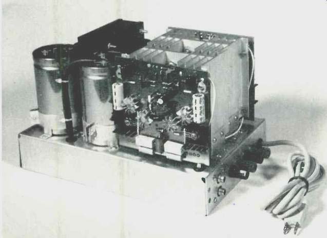
Fig. 1--Photograph of the author's chassis layout. The case on the power
transformer has been changed so that it could be mounted vertically without
the use of L-brackets.
Although there exist no present standards for the measurement of TIM distortion (in a private communication, Prof. Matti Otala of the University of Oulu in Finland has told the author that he is presently constructing a TIM measuring instrument), the susceptibility of an amplifier to it can be determined in some cases with an oscilloscope and a fast rise time square-wave generator. With a square-wave input signal, the signal at the output of each internal stage in the amplifier should ideally be a square wave with little or no overshoot or ringing. Unfortunately, however, in the majority of amplifiers, the internal stage which is most susceptible to TIM distortion is almost always a current gain stage rather than a voltage gain stage. Since an oscilloscope is a voltage measuring instrument, it is almost impossible to observe internal transient overshoot problems in such amplifiers without their modification or the use of expensive current probes.
In this article, a practical design example is presented which is based almost entirely on the design philosophy presented in the previous article.
Since each internal stage in this amplifier utilizes local negative current feedback, the impedance levels in the amplifier are sufficiently high and the feedback ratio is sufficiently low so that the transient response of each internal stage can be measured easily with an oscilloscope. The circuit has been carefully designed so that transient inter-loop signal overload cannot occur, even with ultra-fast rise time square-wave signals applied to the amplifier input. Since no internal stage is subject to transient overload problems, the amplifier is theoretically free of TIM distortion, and the results can be startlingly audible, especially with full-range electrostatic speakers.
When used within its power limitations, the amplifier can be used with the finest associated equipment. In several subjective listening tests, it has audibly equaled or surpassed any amplifier to which it has been compared.
The audible differences are greatest during music which contains loud high-frequency material and percussive sounds. These differences are attributed to the controlled inter-loop transient response of the amplifier and the lack of TIM distortion in the reproduced music. These are principally a direct result of the fact that the open-loop frequency bandwidth is 38,000 Hz or approximately twice that of the audible spectrum.
The amplifier is a fully complementary-symmetry, direct coupled design. It has a closed-loop frequency response which extends from approximately 0.5 Hz to 150,000 Hz. The response outside these limits has been intentionally rolled off. Otherwise, the small-signal frequency response would extend from d.c. to over 800,000 Hz. With the specified power supply, the power output is 70 watts per channel, both channels driven simultaneously, or 84 watts from either channel driven alone.
Both the IM distortion (SMPTE Standard) and the THD are less than 0.2% at 70 watts or less, where the THD is measured at any frequency between 20 Hz and 20,000 Hz. At lower power levels, the distortion is much lower, typically 0.04% or less. However, no ultra-low distortion levels are claimed since an unrealistically low THD specification can indicate the presence of TIM distortion in an amplifier [2]. With the feedback loop disconnected, the amplifier will produce 50 watts into an 8-ohm load with a THD of only 0.5% at 1000 Hz. This low distortion is indicative of the inherent linearity of the open-loop amplifier.
Thus, the addition of negative feedback has not been used to "clean up" problems of the basic design, but to improve it. As the power level is decreased, both the IM distortion and THD decrease monotonically. This indicates the absence of crossover distortion.
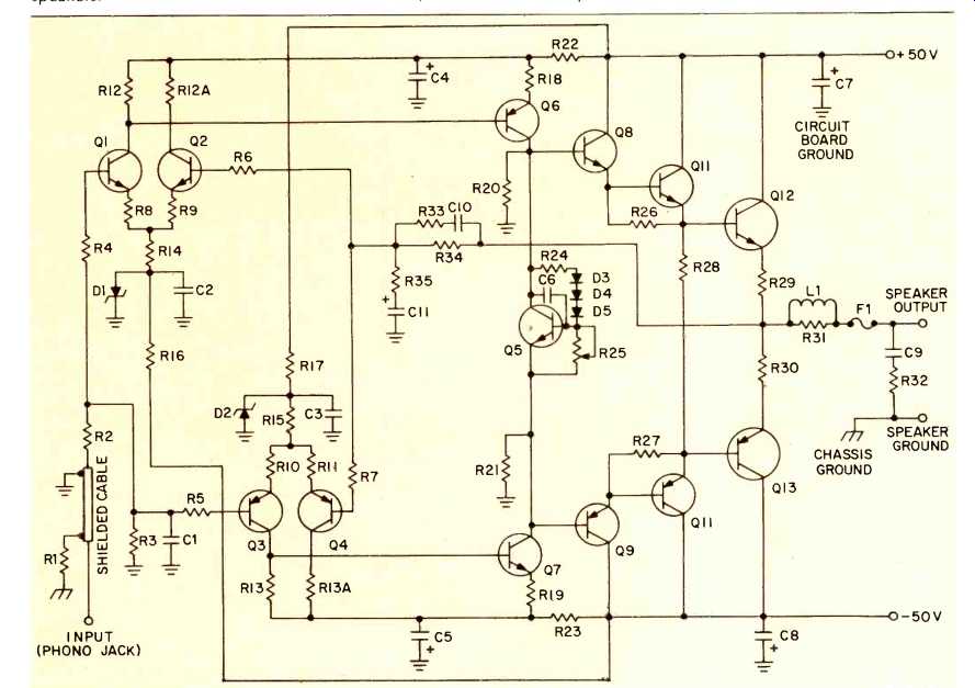
Fig. 2--Complete circuit diagram of one channel.
The damping factor is approximately 250 from 20 Hz to 20,000 Hz. Although this is only moderately high, it does not change appreciably with frequency in the audio band. In contrast, an amplifier with an inadequate open-loop bandwidth will exhibit a damping factor which can change appreciably with frequency, often by a factor as high as 100 or more. A damping factor which is relatively insensitive to frequency indicates that the output impedance of the amplifier is essentially constant and does not vary with frequency. Whether this can be audible is not known, however, it is felt that a frequency-sensitive output impedance can lead to transient problems with certain reactive loads, particularly full-range electrostatic speakers.
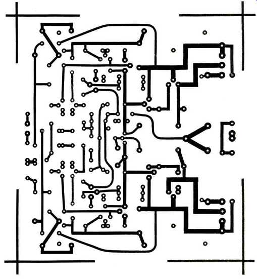
Fig. 3(a)--Circuit side of printed circuit board foil patterns for one channel.
Description of the Circuit
The overall circuit diagram of a single channel of the amplifier is shown in Fig. 2. With few exceptions, the basic configuration is rather conventional. However, each component has been selected specifically to prevent inter-loop transient problems from occurring. In addition, the circuit has been designed for a controlled open-loop gain and bandwidth that are essentially insensitive to frequency variations of the speaker load impedance. The amplifier as presented in Fig. 2 has no protection devices, such as current limiters or VI limiters, as it is felt that these devices represent a compromise in the ultimate sound quality which can be achieved. However, the circuit board has been designed to accommodate a VI limiter which will be described in a later article. For home use, this is not recommended unless the amplifier might be subjected to abuse.
The basic amplifier consists of two stages of voltage gain, three stages of current gain, a temperature-sensing bias regulator, and a feedback network. With the exception of the output transistors, all transistors have been selected from the manufacturer recommended lists published in the current Motorola Semiconductor Master Selector Guide. Thus, they should be easily obtained by those who wish to construct the amplifier from scratch. The output transistors are relatively new units which are manufactured by Texas Instruments.
They are rated at 200 watts and 30 amperes, and they have the necessary minimum breakdown voltage (BVCEO) of 100 volts.
The input stage is a conventional double-ended differential amplifier which has a gain of about 10 to 12.
The complementary transistors Q1 through Q4 in this stage are specifically recommended by Motorola for low-level, low-noise audio frequency applications. The bias current in these transistors is set at 0.6 mA by the Zener diodes D1 and D2 and the emitter bias resistors R14 and R15. Resistors R8 through R11 provide local negative current feedback to linearize the gain characteristics and improve the bandwidth of the input stage. In addition, these resistors, in conjunction with the collector load resistors R12 and R13, set the gain of the input stage.
The input signal is coupled to the differential amplifiers through a lowpass filter which has a nominal 3-dB cutoff frequency of about 150 kHz.
When used with a preamplifier with a 10-kOhm output impedance, the cutoff frequency of this filter will drop to about 50 kHz.
The differential amplifiers have two outputs which are electrically in phase but have a d.c. voltage of about 45 volts between them. These two outputs are connected to the second stage of voltage gain consisting of transistors Q6 and Q7. These transistors are biased at about 4.3 mA, and they provide a push-pull voltage gain of about 45. The gain of this stage is set by the two emitter resistors R18 and R19 and the two collector load resistors R20 and R21. In addition, resistors R18 and R19 provide heavy local negative current feedback for linearity and wide bandwidth.
Fig. 3(b)-Ground plane side of printed circuit board foil patterns for one
channel.
This layout contains the VI limiter circuit which will be described later.
The second voltage gain stage has two outputs which are electrically in phase but are separated by a d.c. voltage of about 3.45 volts. This d.c. voltage is regulated by transistor Q5 which is connected as a constant voltage regulator. The purpose of Q5 is to provide a constant quiescent bias current in the output transistors so that they operate in a true class-AB mode.
Since the quiescent base-to-emitter junction voltage in the output transistors decreases with temperature, it is necessary for a voltage across Q5 to decrease by the same amount if the bias current in the output transistors is to remain constant as they warm up under load. The three diodes in the base bias network for Q5 provide the necessary thermal feedback. They are mounted on the heat sinks with the output transistors so that they will both be in thermal equilibrium. The nominal voltage across Q5 is given by the equation:
V=0.6(1+R24/R25)+1.8 (1)
This voltage will drop by about 6 mV per degree Celsius as the output transistors warm up under load. This provides essentially perfect thermal regulation of the bias current in the output transistors and prevents thermal runaway. From an audible point of view, the bias current is not overcompensated for absolute protection from thermal runaway, for this can lead to the production of crossover distortion in the output stage as the amplifier warms up under load.
Transistors Q8 through Q11 are connected as a complementary Darlington driver stage. Although Darlington transistors are available, they cannot match the bandwidth and thermal stability of the discrete transistors used in the Darlington configuration. All four of the driver transistors are forced to operate in a true class-A mode since their emitter outputs are not connected directly to the speaker output. Since the driver transistors never cut off under load, the driving point impedances seen by the bases of the output transistors remains constant as the output transistors turn off and on in the class-AB mode. Thus, the driving point impedance remains very low during each half cycle of the output voltage swing. This low impedance aids in draining out the charge stored in the base region of the output transistors when they turn off, thus speeding up their turn-off time and improving the open-loop bandwidth of the amplifier.
The class-A driver stage is similar to one described by Locanthi [3] in what the author considers one of the true classic transistor amplifier designs. This is the JBL "T circuit" which was introduced in 1966. To the author's knowledge, this amplifier is no longer being manufactured. A simplified two-transistor version of the "T circuit" driver is used in certain amplifiers currently marked by SAE and the Great American Sound Co.
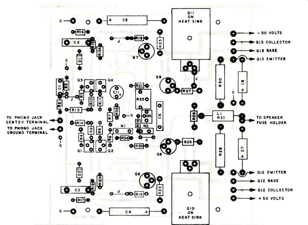
Fig. 4--Circuit board parts layout for one channel. View is from component
side of board.
The complementary output transistors are connected in the emitter follower or common collector configuration for maximum bandwidth.
They operate in a class-AB mode for minimum distortion and minimum power dissipation. In the class-AB mode, both transistors are conducting current during no or very small signal inputs. However, as the input signal level increases, one transistor will progressively conduct more and the other progressively less during any half-cycle of the signal until the latter transistor turns off. Thermal stability has traditionally been a problem associated with class-AB output stages.
However, this problem is completely eliminated in this circuit by the thermally compensated bias regulator.
The regulator will maintain a constant bias current in the output transistors as the heat sinks warm up from no load to their maximum temperature.
This occurs at approximately 40% of the maximum output power. The 0.22-ohm resistors in series with the emitters of the output transistors serve two purposes. First, they provide local negative current feedback for linearity. Second, they protect the output transistors from an accidental short circuit across the speaker output terminals. For short circuit protection, these resistors must be fused resistors such as those manufactured by Workman.
The feedback network consists of resistors R33, R34, and R35, and capacitors C10 and C11. For all audible frequencies, C11 is a short circuit and C10 is an open circuit. Thus, the amplifier gain is given by
G=1+R34/R35 (2)
or 26 dB.
Below 1 Hz, C11 becomes an open circuit. This reduces the d.c. gain of the amplifier to unity to insure d.c. stability. Between 150 kHz and 800 kHz, C10 becomes a short circuit, thus increasing the high-frequency feedback ratio. This lead compensates the amplifier by increasing the high-frequency loop gain. By performing the lead compensation in the feedback network, optimum inter-loop transient response is obtained and, simultaneously, the closed-loop frequency response is rolled off.
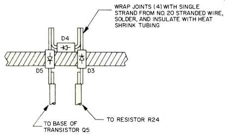
Fig. 5--Diagram showing proper mounting of the temperature compensating
bias diodes on the main heat sinks.
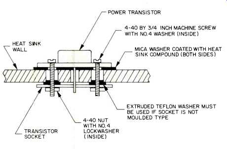
Fig. 6--Diagram showing proper mounting for transistors Q12 and Q13 on the
main heat sinks.
Construction
Although straightforward, construction of the amplifier requires care if it is to be done properly. The construction details are broken into two parts. In this section, the circuit board/heat sink assembly is discussed; in the following section, the chassis construction details are presented. Before construction is begun, all parts should be assembled so that the layout can be modified to accommodate any parts which may have different dimensions from those used by the author. The printed circuit board is a double-clad board, one side of which is used as a ground plane for the circuit. Ground-plane construction is standard practice in r.f. amplifiers, and it is highly recommended for this amplifier. The front and back printed circuit board layouts are shown in Fig. 3. The parts locations on the boards are shown in Fig. 4.
Care must be taken when laying out the board to insure that the layouts on both sides align. This is relatively simple since the only areas which must be etched on the ground plane side are circular pads through which the component mounting holes are drilled. First, prepare a negative for the circuit side of the board using standard PC layout techniques. Second, tape a clear sheet of mylar over the component side of this negative.
Then place 0.125-inch adhesive circular PC layout pads on the mylar, carefully aligning one over each of the solder pad locations on the negative. There are 12 solder pad locations on each board which should not be covered with the circular pads. Six are used for connections from the circuit side of the board to the ground-plane side. The others locate the mounting screws for transistors Q10 and Q11 and the four mounting screws for attaching the PC board to the heat sink.
After the mylar sheet is prepared, it can be used "as is" for exposure of the ground plane side of the board.
However, it is preferable to make a photographic positive (i.e. double negative) of the layout to expose the board with.
To expose the board, first tape the two negatives together along two opposite edges after the two-sided layout has been carefully aligned. Be sure that the circuit side of each layout is on the outside. Otherwise, a mirror image circuit will result. Under dim yellow light, insert a double-clad, photosensitized blank board between the negatives. Next tape the negatives to the board along two opposite edges on both sides of the board. The negatives should now be properly aligned on the board, and it can be exposed one side at a time under ultraviolet light. If the board is developed in a flat pan, care should be taken not to scratch the fragile photoresist on the bottom surface of the board.
The best rule to follow is not to rock the developing tray enough to cause the board to slide, otherwise the photo-resist will be scratched. A spray developer or vertical developing tank will eliminate these problems. After the board has been developed, it can be etched and cut to size along the crossed lines which locate its four corners. All component mounting holes should next be drilled to the proper diameter. Too large a drill bit will lift the copper solder pads from the board, so care should be exercised.
The four mounting screw holes for the board and the two mounting screw holes for transistors Q10 and Q11 should be drilled for a 4-40 screw.
The next step is to solder the six ground connections on each board.
To do this, bend a 5/8-inch length of No. 20 solid wire into a 1/8 by 1/2 inch L-shape. Insert the wire through a ground hole with the 1/8-inch side against the ground plane. Solder the wire to the ground plane with a 100 watt soldering gun. To prevent the solder from running, do not touch the ground plane with the gun tip, but hold it against the wire and parallel to the ground plane. While applying heat, feed solder to the tip until it fills the gap between the tip and ground plane, then lift the gun from the board. The resulting solder joint should then be in the form of a circular pad which firmly bonds the wire to the ground plane. The ground wires on the reverse side of the board can now be soldered and clipped.
After the ground wires are soldered, the boards should be thoroughly cleaned and the ground-plane side sprayed with a good brand of clear lacquer to prevent corrosion. Before spray painting the boards, cover the four screw mounting holes which are used to attach the boards to the heat sinks with 3/8-inch circular adhesive pads to prevent the paint from insulating the areas where the mounting screw heads make electrical contact to the ground plane. After the paint is dry, the circuit side of the boards can be plated to prevent corrosion if desired. If a water-soluble tin-plate solution is used, the temperature of the solution should not be so high as to cause the painted ground plane surface to peel.
Fig. 8--Circuit diagram of the power supply.
The next step is to mount and solder all components to the boards using Fig. 4 as a reference. Care should be taken to insure that all transistors, diodes, and electrolytic capacitors are mounted exactly as shown in the figure and that no component leads come in contact with the ground plane. It is necessary to use mica washers and heat sink compound between transistors Q10 and Q11 and their heat sinks. These transistors should be secured to the board with 4-40 by 1/2-inch screws, lockwashers, and nuts. The screws should be tightened only enough to engage the lock washers, otherwise the transistors may be damaged. The parallel combination of R31 and L1 is formed by tightly winding a length of insulated No. 20 solid copper wire around a 2.7 ohm, 2-watt resistor and soldering it to the resistor leads. All components should be mounted flush with the board except transistors Q1 through Q9, R29, and R30. These should be mounted 1/4 inch above the board. A TO-5 heat sink should be installed on each of transistors Q6 through Q9.
The next step is to prepare the temperature compensating diode assemblies. These must be mounted in holes drilled in the heat sinks between the power transistors as shown in Fig. 5.
The holes should be just large enough for the diodes to fit as snugly as possible. The diodes can be any general purpose silicon rectifier diodes with an epoxy (not glass or metal) case. Be fore soldering the diode bias assemblies together, install the diodes in the holes in the heat sinks, as shown in Fig. 5, and wrap a single strand of wire from No. 20 stranded wire around the leads to hold them together. The diode bias assembly can now be soldered together in place. It is very important to insulate all solder junctions with heat shrink tubing to prevent them from coming in contact with the grounded heat sinks. The leads from the diodes to the circuit board should be 6 inches long, and they should be twisted tightly together before they are soldered to the board from its circuit side. These leads should be No. 22 stranded wire, and they should be color coded to indicate the cathode and anode sides of the diode assembly.
Each power transistor should be installed on the heat sinks using a TO-3 insulating heat sink washer, a TO-3 transistor socket, and two firmly tightened 4-40 by 3/4-inch screws with lock washers and nuts. If mica insulating washers are used, both sides should be liberally coated with heat sink compound. The newer and more efficient silicon rubber washers do not require a heat sink compound, and they are recommended. If the transistor sockets are not of the molded type, it is very important to insulate the 4-40 screws from the heat sinks with extruded Teflon washers. Remember that the case of the output transistors and their mounting screws are at the full power supply voltage.
Therefore, extreme care should be taken to insulate them properly from the heat sinks. The proper mounting of the output transistors is illustrated in Fig. 6. After the sockets are installed, solder a 6-inch length of No. 20 stranded wire to each of the three terminals on each socket. These can now be soldered to the correct points on the circuit side of the board. Before mounting the circuit boards to the heat sinks, solder a 16-inch length of No. 20 stranded wire to the speaker output lead and an 8-inch length of No. 20 stranded wire to the +50 volt power supply input and the-50 volt power supply input on each circuit board. These wires should all connect from the circuit side of the board, as do the leads from the diode bias assemblies and output transistors.
The circuit boards can now be mounted to the flanged edges of the heat sinks with four 4-40 by 3/4-inch screws, four nuts, and eight lock washers (one under each screw head and one under each nut). A 1/2-inch insulating sleeve must be placed on each mounting screw between the circuit board and the heat sink to provide the necessary clearance between the two. The mounting screws should be tightened sufficiently to firmly engage the lock washers, for it is through them that the ground connection for the circuit boards is made.
The Chassis Figure 1 shows the amplifier constructed on a 7 x 11 x 2-inch chassis.
The top of the chassis contains the two circuit board heat sink assemblies, the power transformer, and the two filter capacitors. The rear panel contains the four speaker output terminals, the phono input jacks, and the feedthrough hole for the a.c. power cord. Although not visible in the figure, the front panel contains the a.c. power switch and the two speaker fuse holders. The underside of the chassis contains the bridge rectifier, a five-lug terminal strip, the a.c. power line fuse clip, and four fuse clips for fusing the d.c. power supply leads to each circuit board. The layout of these components is shown in Fig. 7.
The first step in assembling the chassis is to drill all chassis mounting holes and mount all components with the exception of the circuit board/heat sink assemblies. As shown in Fig. 1, the two heat sinks are mounted 1/2 inch above the chassis on L-brackets which can be fabricated from 1/16-inch sheet aluminum. The heat sink fins are interleaved to conserve space. In addition, this creates a chimney effect to aid in the circulation of air through the heat sink assemblies. For adequate cooling, the heat sinks should not be mounted closer than 1/2 inch to the chassis. In addition, the outer two edges of the heat sinks should not be closer than 1-1/4 inches from the edge of the chassis. This will allow sufficient room to mount the circuit boards on the heat sinks without their components overhanging the edge of the chassis.
A total of four 3/8-inch holes should be drilled in the top of the chassis, and rubber grommets installed in them. One hole adjacent to the filter capacitors carries the four leads from the power supply to these capacitors. One hole directly above the phono input jacks carries the two signal input leads from the jacks to the circuit boards. One hole centered 1 inch behind each circuit board carries the two power supply leads and speaker output lead for that respective channel.
Fig. 9--Transistor lead connections.
The power supply circuit shown in Fig. 8 uses a single ground point for all high current leads to minimize hum and ground-loop problems. The ground point used in Fig. 8 is the center ground lug of the terminal strip.
To this point are connected the power transformer secondary center-tap lead, the two filter capacitor ground leads, and the two speaker ground leads. To further minimize ground loop problems, the ground terminal of each phono input jack is isolated from chassis ground by a 2.7-ohm resistor. Although insulated phono jacks are available, the phono jacks and 2.7 ohm resistors for the unit in Fig. 1 are mounted on a small printed circuit board behind the rear panel of the chassis. Ground connection to the circuit board is made through two of the 4-40 by 1/4-inch mounting screws, lockwashers, and nuts.
After drilling all mounting holes in the chassis and installing grommets in the appropriate ones, the power transformer, filter capacitors, phono jacks, speaker output connectors, a.c. power switch, speaker fuse holders, power supply fuse clips, bridge rectifier, and terminal strip should be mounted on the chassis. Lock washers should be used under all nuts, and the mounting screws should be tightened securely. The chassis is wired with No. 18 and No. 20 stranded wire. Red and black color-coded leads are recommended to distinguish between the ground and different polarity leads.
No. 18 wire should be used for all leads to and from the filter capacitors and bridge rectifier. No. 20 wire should be used for all power supply leads from the fuse clips to the circuit boards and for all speaker leads.
After the power supply has been wired, the circuit board/heat sink assemblies can be mounted on the chassis and wired to the power supply fuse clips and the speaker fuse holders. The No. 20 wires for these connections should have already been soldered to the circuit boards. After this is done, the speaker output connectors can be wired to the speaker fuse holders and the chassis ground connection on the terminal strip. No. 20 stranded wire should be used for these connections. To make the wiring neater, the two power supply leads to each circuit board should be twisted together before soldering them in place, as should the two wires to and from each speaker fuse holder and the two speaker ground wires.
Across the speaker output terminals of each channel, a 10-ohm, 2-watt resistor in series with a 0.1 microfarad capacitor should be soldered. These should be connected and insulated so that it is impossible for the solder junction between the resistor and capacitor to accidentally come in contact with a hot terminal under the chassis.
Cable ties are recommended to bind the transformer and filter capacitor leads as shown in Fig. 7. In addition, an insulated strain-relief feed through or a grommet and insulated strain-relief clamp should be used to prevent the a.c. power cord from being accidentally pulled from the amplifier. This will also insulate the power cord jacket from the sharp metal edges of its feedthrough hole.
The final step is to connect the shielded phono cables from the phono input jacks to the circuit boards. These cables should not be routed near any speaker or power supply lead, otherwise oscillations could occur due to mutual coupling between the leads. The input cables should be routed through the chassis hole above the phono jacks, up the outer edge of the circuit board/heat sink assemblies as shown in Fig. 1, and soldered to the rear of the circuit boards. After this step is completed, all wires connecting to the rear of the boards should be checked to see that they do not make contact with any component on the ground plane side of the board. If any of these wires protrude through the boards to the ground plane side, they should be clipped flush with the board.
Initial Turn-On and Adjustments
Before any attempt is made to apply power to the amplifier, it is strongly recommended that the entire unit be checked very carefully for errors. All solder joints, transistor and diode lead connections, and polarity of electrolytic capacitors should be checked especially. If everything appears to be correct, the initial tests can be performed. First, install the a.c. power fuse. Do not install the four d.c. fuses to the circuit boards at this point. Plug the a.c. power cord into a Variac auto transformer, turn the amplifier on, and slowly increase the a.c. voltage with the Variac while monitoring the + and d.c. outputs of the bridge rectifier. The two voltages should have equal magnitudes, and the polarities should be correct. If both filter capacitors are polarized correctly, the a.c. voltage can be increased to 120 volts. (Do not increase the Variac above that value.) The positive and negative d.c. power supplies should then read within one or two volts of 50 volts. The a.c. power can now be removed and the filter capacitors discharged by holding a 1-kOhm resistor across the terminals of each until the voltage falls to zero.
In the next test, d.c. power is applied to each circuit board individually. Before proceeding, adjust potentiometer R25 for maximum resistance, i.e. 5 kOhm. This should be verified with an ohmmeter, otherwise the power transistors may be damaged in the next test. Install the two fuses for the d.c. power to one channel. Connect a 1-kHz signal of amplitude 1 volt rms to the input of that channel and an oscilloscope to its speaker terminals. Do not connect any other load to the amplifier. With the a.c. power switch on, slowly increase the a.c. voltage with the Variac until the output signal is observed. The signal will initially appear as a clipped sine wave.
There should be no d.c. voltage on the speaker terminals. The a.c. voltage should not be increased by more than about 10 volts at a time without feeling each transistor in that channel including the output transistors for overheating. If any transistor becomes hot to the touch, immediately remove the a.c. power, for the circuit contains a wiring error or has a defective component.
If no transistor overheats, the a.c. voltage can be increased to 120 volts.
The sine wave output should no longer appear clipped, and its amplitude should be 20 volts rms or about 56 volts peak-to-peak. The a.c. voltage can be reduced to zero and the other channel tested similarly after first discharging the filter capacitors with a 1-kOhm resistor.
If the preceding tests are successful, the bias potentiometers (R25) can be adjusted next. With no input signal or load on either channel, turn the amplifier on and decrease R25 until the voltage across Q5 is 3.45 volts on each channel. A d.c. voltmeter with a floating ground should be used for this adjustment. The voltmeter leads can be clipped to the heatsinks on transistors Q6 and Q7, for the collectors of these transistors are connected across Q5. While adjusting R25 for a 3.45 volt reading, alternately feel each output transistor in that channel for overheating. If either output transistor begins to warm up, that channel is defective or the d.c. voltmeter is not calibrated correctly. When R25 is properly adjusted, the heat sinks on which the output transistors are mounted will be barely warm to the touch after the amplifier has idled for approximately 30 minutes.
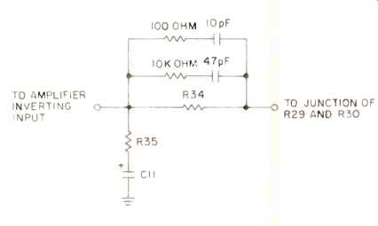
Fig. 10-Circuit diagram of the alternate feedback network.
Table I-Parts List for power supply and one channel. All resistors are 1/4 watt, 5% unless otherwise specified.
All resistors are 1/4 watt, 5% unless otherwise specified.
R1-2.7 ohm
R2-2.7 kOhm
R3-33 kOhm
R4, R5, R6, R7-1 kOhm
R8, R9, R10, R11-100 ohm
R12, R13, R12A, R13A, R16, R17-3.9 kOhm
An alternative adjustment of R25 [...to be cont.]
(adapted from Audio magazine, Feb. 1976)
Also see:
Amp Design and Overload (Nov. 1977)
= = = =