by ROBERT R. CORDELL
The Total Harmonic Distortion (THD) analyzer is probably the most widely used instrument for evaluation of distortion in audio systems.
Unfortunately, those analyzers which are good enough to evaluate contemporary equipment generally cost in the neighborhood of $2,000. Because of a careful selection of features and a topology which lends itself to realization with low cost components, the analyzer de scribed in this article can be constructed for a fraction of that cost, while providing a measurement floor on the order of 0.001 percent across the full audio band.
A typical measurement setup of a THD analyzer is shown in Fig. 1. It consists of a low-distortion oscillator feeding the Unit Under Test (UUT) which in turn feeds the THD analyzer; an oscilloscope is optionally used to observe the wave form of the distortion products. (In most high-performance THD analyzers, the oscilloscope and analyzer are in one unit.) It is well known that a nonlinearity in the UUT, when adequately excited by a sine wave (the so-called "fundamental"), will produce at the output harmonics of the sine wave in addition to the fundamental. The principle of the THD analyzer is to remove the fundamental entirely and measure what is left. This removal of the fundamental is usually achieved with an extremely sharp and deep notch filter centered on the fundamental frequency.
The 'scope photo in Fig. 2 shows the fundamental sine wave in the top trace and a typical distortion waveform in the bottom trace. Viewing the distortion in the "time domain" is very useful in evaluating the nature of the distortion mechanism. Here, the disturbances near the zero crossings of the fundamental imply that crossover distortion exists. As far as audibility is concerned, for a given magnitude of distortion, smooth or "soft" distortion waveforms are preferable to jagged or "harsh" waveforms.
How THD Analyzers Work
We can get a feel for some of the analyzer requirements by seeing what the desired performance specification implies. Here, our goal is a measurement floor of less than 0.001 percent. This means that if we bypass the UUT, that which remains after the fundamental is rejected is less than 0.001 percent, or 100 dB down. The residual will consist of distortion, un-rejected fundamental, noise and hum. Clearly, we need a very good oscillator, one with distortion at least 10 dB down from the floor, or better than 0.0003 percent. In addition, low-noise, low-distortion electronics throughout the analyzer are mandatory.
Similarly, the notch filter should probably have at least 110 dB of rejection, while attenuating the closest harmonic (the second) by less than, say, 0.5 dB. Such a sharp notch is normally difficult to achieve and even more difficult to tune manually. This problem is dealt with in most high-performance analyzers by automatic tuning circuits, often termed "auto tune". Notch filters are generally realized by passing the signal through two paths with differing phase and/ or amplitude characteristics so that the two resulting outputs are equal and of opposite phase only at the center frequency. When combined, the signals thus cancel each other at the center frequency. It can be seen that an automatic tuning system must exert two types of control: One to assure the proper phase relationship at the notch frequency, and one to assure that the amplitudes of the two signals are exactly equal at the notch frequency so that full cancellation can occur. As we shall see later, these two control circuits each function by examining different characteristics of the output of the notch filter and then adjusting notch filter control elements accordingly. The auto-tune circuits of a THD analyzer are generally responsible for a substantial portion of the overall cost, but they are virtually indispensable. With well-designed auto-tune circuits, rejection of the fundamental is so complete that analyzer internal distortion and noise generally dominate the residual and establish the measurement floor.
To make maximum use of the convenience associated with auto tune, it is best to have the oscillator packaged in the analyzer so that its frequency can be controlled in step with that of the analyzer. This also tends to reduce the control range required of the auto-tune circuits, making them less prone to limit analyzer performance.
An additional feature found in most better analyzers is called "auto set level." In analyzers without this feature, a level-setting calibration adjustment must be made whenever the input level is changed. An auto set level feature permits the input level to the analyzer to change over some range, say ± -10 dB, without affecting the calibration of the distortion meter. It is achieved with a type of a.g.c. circuit which adjusts the gain in the measurement path (after the notch filter) downward in direct proportion to increases in input level.
Finally, many analyzers include high pass and low-pass filters of varying complexity and flexibility to optimize performance. These distortion product filters are placed in the measurement path after the notch filter. Generally, a high-pass filter is used to minimize the effect of hum in the UUT on the measurement.
Low-pass filters are usually employed to limit the measurement bandwidth (to minimize noise) while passing all of the harmonics of interest (e.g., up to the tenth).
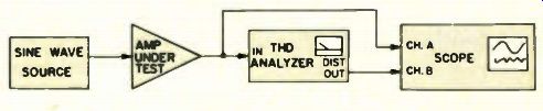
Fig. 1 - Typical measurement setup of a TI-11) analyzer.
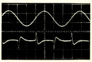
Fig. 2 - 'Scope photo showing the fundamental sinc wave (top trace) and a typical crossover distortion waveform (bottom trace).
Practical Analyzer Design
My goal here was to provide a THD analyzer design capable of state-of-the art performance which can be constructed at moderate cost and with readily available parts. At the same time, I felt that retaining the features of a built-in oscillator, auto tune, auto set level, and product filtering was essential. One com promise made to keep down costs was to limit the number of switch-selectable operating frequencies to 10 evenly spaced frequencies per decade from 20 Hz to 200 kHz. Another cost saving resulted from the extensive use of ICs, even in the most critical circuits. In particular, the superb distortion performance of the 5534 operational amplifier made this possible.
A major expense in many analyzers is due or related to the control elements in the auto-tune circuits. The use of so called "state-variable filters" in both the oscillator and the notch filter in this analyzer permitted the use of inexpensive FETs as the control elements in these circuits. The greater immunity to control element nonlinearities of these filters has been pointed out. The topology of these filters also permits the use of ± -10 percent capacitors where precision components would normally be required.
While several sets of four identical range-selection resistors must be matched to within ± -1 percent, the absolute value of these resistors is not critical.
Thus, a patient constructor with a digital VOM or simple resistor bridge can select matched sets from standard 5 percent carbon-film resistors. It's highly unlikely that you won't find four or more resistors matched to within ±1 percent among a group of ten - ±5 percent carbon-film resistors purchased at the same time.
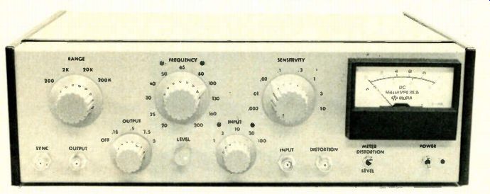
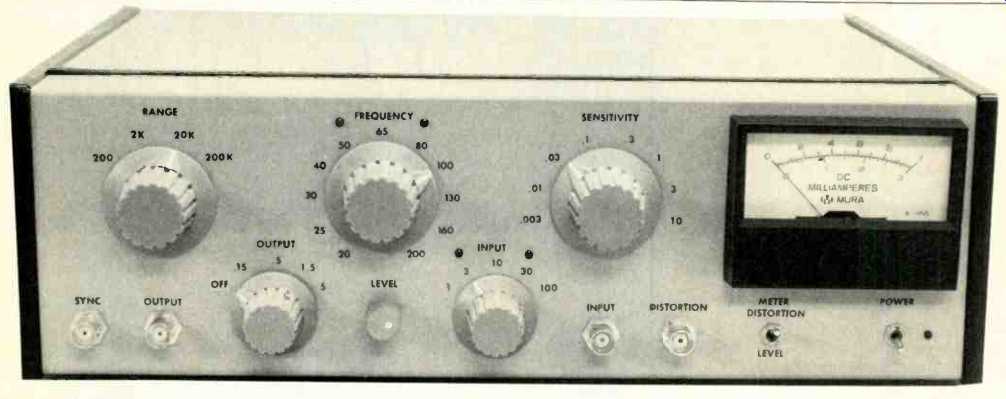
The exterior and interior views of the completed analyzer are shown in Figs. 3 and 4. The circuitry of the analyzer re sides on one small and two medium sized single-sided printed circuit boards; the regulated power supply is housed in a small metal box at the rear. As can be seen from the photo in Fig. 4, the major part of the construction effort is in the range and frequency switch wiring. As a guide to cost, the three circuit boards and their associated components will typically cost about $160. The cabinet, power supply, meter, switches, switch mounted components, etc. will represent additional expenses.
Before proceeding, one word of caution is in order. This ambitious and moderately expensive project should not be attempted by anyone who has not previously built and troubleshot electronic construction projects. Anyone who does not own or have access to an oscilloscope should also think twice before embarking on it. This is a challenging construction project requiring consider able effort and patience, but the payoff is great for anyone who wants a THD analyzer with state-of-the-art performance.
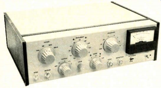
Fig. 3 - Exterior view of the completed THD analyzer.
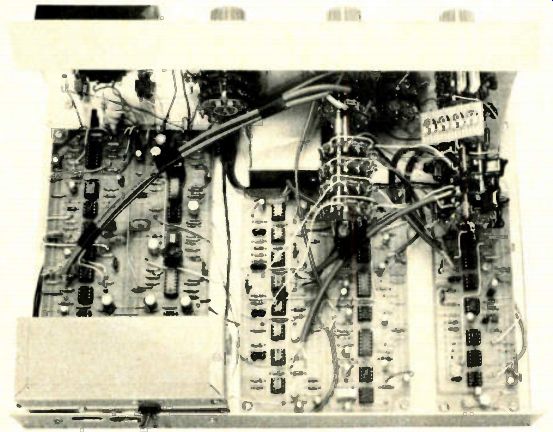
Fig. 4 - Interior view of the THD analyzer.
Overall Design
A block diagram of the complete analyzer is shown in Fig. 5. We'll now proceed with a brief overview of the analyzer's operation at the block diagram level before moving on to more detailed descriptions of the individual circuits.
The signal source resides on a single p.c. card, CP1, and consists of a state variable oscillator, the necessary amplitude stabilizing circuits, an output amplifier, a level control, and an output attenuator. The amplitude control circuit is essentially a level detector which generates a d.c. error signal to feed the amplitude control multiplier. The latter controls the amount of positive feedback in the oscillator and consists of an FET and an operational amplifier.
The input circuits, controllable notch filter, auto-set level circuit, and distortion product amplifiers are located on a second p.c. card, CP2. The notch filter consists of a differential amplifier which is fed the input signal and a version of this signal which has passed through a state variable bandpass filter whose frequency and gain are controlled electronically. At the center (fundamental) frequency, both inputs to the differential amplifier we identical in phase and amplitude, leaving only the distortion products at its output.
The bandpass filter is sufficiently narrow that its output is very small at the second harmonic and higher frequencies, resulting in less than 0.5 dB of attenuation at the second harmonic. Operation of the notch filter is illustrated by the frequency response curves in Fig. 6.
The auto-set level circuit consists of two voltage-controlled amplifiers (VCAs) to which are fed identical control signals so that their gains vary in the same fashion. One VCA is in the path of the distortion product signal, while the other ("reference" VCA) is fed the output (the filtered fundamental) from the state-vari able bandpass filter. The latter VCA feeds a level detector whose d.c. output controls both VCAs. The a.g.c. loop formed by the level detector forces the output of the reference VCA to be at a fixed reference level. Thus, if the input signal level doubles, the gain of both VCAs will be halved, resulting in the proper gain correction being applied to the distortion product path. Both VCAs are realized from inexpensive 1496-type balanced modulator ICs and achieve a control range of ± - 20 dB with better than ± 0.5-dB tracking. Notice that the distortion performance of the VCAs need not be exceptionally good because the one in the measurement path is passing only distortion products. Placement of an a.g.c circuit ahead of the notch filter would necessitate the use of an extremely low-distortion VCA and might also compromise the noise floor of the instrument.
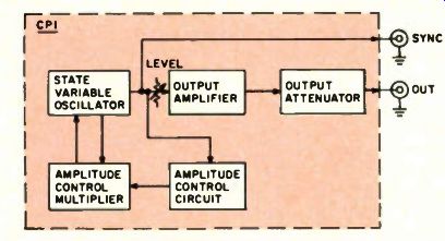
Fig. 5 - THD analyzer block diagram.
The auto-tune control circuits, product filters, status indicator circuit, and meter amplifier are located on a third p.c. card, CP3. The auto-tune control circuits consist of amplitude and frequency detectors which produce d.c. error signals to control the gain and center frequency of the state variable bandpass filter. These detectors function by looking for small amounts of fundamental in the output of the notch filter.
The principle of operation is as follows: An amplitude error between the two signals at the inputs of the differential amplifier will result in a small amount of in-phase (or 180-degree out-of-phase) fundamental at the output of the notch filter The polarity of this error signal indicates which direction of amplitude adjustment is necessary Similarly ,but less obviously, a frequency error in the band pass filter will result in a phase error between the two signals at the differential amplifier This will result in a small amount of fundamental component at the output of the notch filter whose phase is lagging or leading 90 degrees (quadrature) relative to the fundamental Whether the component is lagging or leading indicates which direction of frequency adjustment is necessary Each detector functions by comparing the output of the notch filter (after the auto-set level VGA) to a version of the fundamental supplied by the bandpass filter The amplitude detector looks for in-phase fundamental components by making its comparison with an in-phase version of the fundamental supplied by the bandpass filter .Similarly, the frequency detector looks for quadrature fundamental components by making its comparison with a 90-degree phase shifted version of the fundamental, also conveniently supplied by a different output of the bandpass filter. The ready availability of this quadrature fundamental signal is an additional advantage of the state-variable filter.
The d.c. control signals from the level and frequency detectors also feed a status indicator circuit. This circuit drives front panel LEDs which indicate whether the input signal is too high or too low and also whether the input frequency is too high or too low (useful when a source other than the internal oscillator is used). The high-pass and low-pass product filters in this design are both second-order (12 dB/octave) designs whose cut off frequencies track changes in the selected fundamental frequency. These tracking filters substantially improve the measurement floor and simplify use of the analyzer by automatically providing optimal filtering regardless of the fundamental frequency setting.
The high-pass filter falls off at 12 dB/ octave below the second harmonic frequency. Its roll-off shape is chosen so as to have a minimal effect on distortion product frequency response. The low pass filter is a second-order Bessel de sign which is down 3 dB at the tenth harmonic frequency. The excellent phase response characteristic of this de sign minimizes waveform distortion of the distortion products, preserving the accuracy of the visual display. The analyzer's overall distortion product frequency response is shown in Fig. 7.
While requiring little in the way of electronics, these tracking filters do add substantially to the complexity of the frequency and range switches, and some builders may prefer a simpler and less expensive alternative. Such an approach, providing the fixed filtering at 400 hz, 30 kHz, and 80 kHz found on many commercial analyzers, is also de scribed later in this article.
As a convenience, notice that with the flip of a switch (S6), the input level can be directly read with the range selected by the analyzer's input attenuator.
Fig. 6 - I Notch filter operation. Fig. 7 - THD analyzer frequency response. Fig. 8 - A simple state variable bandpass filter
State-Variable Filters
Because it is central to the operation of the analyzer, a few words of explanation regarding the state-variable filter are appropriate at this point.
A simple state-variable bandpass filter is shown in Fig. 8. It consists of two integrators and an inverter connected in a loop. An input resistor (R1 ) and a second feedback loop ( RB) around the first integrator (Al) complete the filter.
The term "state variable" comes from linear system theory involving solutions to linear differential equations. The state of such a system at a given point in time is completely determined by the values of the system's state variables. The state-variable filter models a second-order differential equation in much the same way as one would model such an equation on an analog computer. In this context, the state variables are the output voltages of the two integrators.
A key to understanding the state-vari able filter is the recognition that an integrator has a frequency response which decreases with increasing frequency at 6 dB/octave and introduces a 90-degree lagging phase shift at all frequencies. Let's temporarily ignore the input resistor R and the bandwidth-setting resistor Re and assume that we have a 1-V, 1-kHz signal at the output of Al.
Each integrator is formed by a resistor (Al = R2), a capacitor (C1 = 02), and an operational amplifier. The gain of the integrator is equal to 1 /(2 pi F1Cf), where f is the frequency of interest and R and C are the values of R1, R2, C1 and 02. R and C are chosen here for an integrator gain of unity at our 1-kHz operating frequency. The inverter also has a gain of unity. Notice that as the 1-V signal travels around the loop, it picks up 90 degrees from each integrator and 180 degrees from the inverter for a total of 360 degrees, which is the same as zero degrees. Thus, at 1 kHz the signal from A3 feeding the Al integrator is exactly the signal required to provide and sustain the assumed output. We therefore have an oscillator.
Looking at it from a slightly different view, the feedback from A3 produces a current in R1 which is just equal to the current required by C1 given the assumed signal at the output of Al. The currents into and out of an ideal op amp's virtual ground (the inverting input when the noninverting input is grounded) must always equal each other.
We can think of an oscillator as a bandpass filter with infinite Q. What if we want finite CY? We add resistor RB, often called the damping resistor. We now need an input, so R is also added. If we make the same assumptions as before, we see that the current in R1 still balances that in C1 at 1 kHz. The current in Re must therefore come from the input via R, so the voltage gain at 1 kHz (the center frequency, f o) is RB/R, and the phase shift is 180 degrees.
At higher frequencies the current demanded by C1 increases and that provided by R1 decreases. The input must now supply the extra current for C1 as well as that demanded by Re. A larger input is thus required for a given output, corresponding to decreased gain. By a similar argument, the gain can be seen to decrease at frequencies below f o as well. We thus have a bandpass characteristic. The 0 of this filter is proportional to the value of Re. The center frequency, f., will always be the frequency at which the gain around the main loop is unity.
This means that the center frequency can be conveniently changed by altering R, C, the inverter gain, or any combination of these.
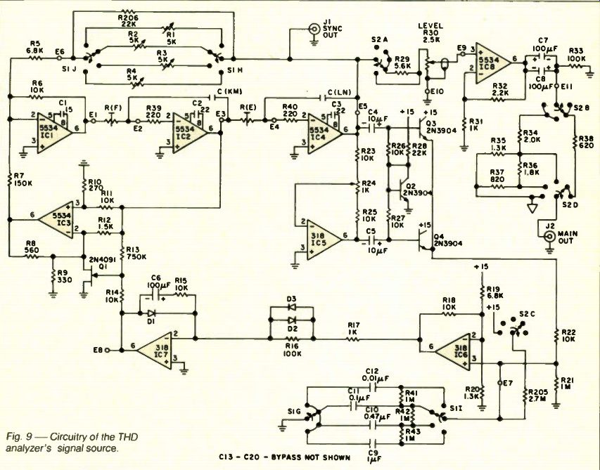
Fig. 9 - Circuitry of the THD analyzer's signal source.
With a bit more reasoning, it is easy to demonstrate that the output of the second integrator (A2) provides a 12 dB/ octave low-pass characteristic. Notice that the phase of this output lags that of the bandpass output by 90 degrees at all frequencies. This feature is used to provide the required 90-degree phase shifted fundamental signal to the frequency detector in the auto-tune circuit.
The Signal Source With a solid understanding of the state-variable filter, operation of the state -- variable oscillator is quite simple.
As in the earlier example, we remove R1 and RB as a start.
As with any linear oscillator, we must provide a means to control the amplitude of the oscillations, i.e., provide a type of a.g.c. circuit. Recognizing that the presence of RB produced negative feedback around the first integrator which tended to damp out oscillations, we can reason that a feedback circuit around Al which can provide variable amounts of negative or positive feedback will allow us to control the oscillations. Negative feed back will cause the oscillations to decay, while positive feedback will cause them to grow. This can be accomplished with a multiplier and a resistor in place of RB. To complete the oscillator, we must add a control circuit to measure the amplitude of the oscillations, then compare it to a fixed reference, and finally deliver a d.c. error signal to the control input of the multiplier.
The complete schematic of the signal source is shown in Fig. 9. First, a word about notation and conventions used on the schematics in this article. For simplicity, power-supply bypass capacitors and power-supply connections to standard pin-out operational amplifiers (+15 V to pin 7, -15 V to pin 4) are not shown.
Off-board interconnection terminals are designated with an "E" number. Terminals on different boards which are connected together have the same E designation.
Each pole of a multi-pole rotary switch is designated with a letter, beginning with "A" closest to the front panel.
Wafers with two poles have the left-hand pole (as viewed from the front panel) designated with the earlier letter in the alphabet; the letter for the right-hand pole is next in the alphabet. Arrows on switch wipers indicate clockwise rotation as seen from the front panel. Tuning resistors are designated by the letter of the switch pole on which they are mounted (each resistor is mounted between adjacent switch positions on a given pole). Tuning capacitors are mounted between two adjacent wafers on the range switch, and they are designated by the letters corresponding to the two switch poles to which they connect.
Because of the large amount of wide band gain packaged in this unit, specific approaches have been taken in terms of grounding and shielding strategy to avoid oscillations and interference pick up. Much of this is shown on the schematics to permit easy duplication.
The 47 symbol, one of three different grounding symbols on the schematics, denotes a single-point chassis ground located at the input jack. All leads with this symbol are connected directly to this single point. The 4% symbol denotes a secondary single-point signal ground on CP2 (Figs. 12 and 13, Part II). This ground is connected to the single-point chassis ground via the shield of the input lead to CP2. The -4- symbol denotes ordinary multi-point circuit grounding.
Each circuit board has its ordinary circuit ground connected to the single-point chassis ground, and positive and negative supply voltage is also distributed on a single-point basis from the location of the single-point chassis ground.
Returning to the circuit discussion, the oscillator proper in Fig. 9 consists of 101 (inverter), 102 and 104 (integrators). Frequency-setting resistors R(F) and R(E) are mounted on frequency switch S3, while the corresponding capacitors C(KM) and C(LN) are mounted on range switch Si. Notice that the circuit has been slightly rearranged from that of Fig.
8, with the inverter "up front" and with the amplitude control feedback (103) en compassing both the inverter and the integrator. This arrangement permits frequency changes to be made by changing the switch-selected resistors without altering other operating characteristics of the oscillator. The analog multiplier for amplitude control is realized by op-amp 103 and FET 01. Notice also that each range has its own frequency trimmer (R1 to R4) to allow close matching of the oscillator frequency to that of the analyzer notch filter without requiring precision frequency-setting capacitors.
The output of the oscillator is taken from 104, which would correspond to the low-pass output of the filter in Fig. 8.
This provides lower distortion and points to a significant advantage of the state variable approach. Given low-distortion amplifiers, the dominant distortion in an audio oscillator results from nonlinearity in the amplitude control element (here the multiplier) and ripple in the " d.c." control signal as a result of the detection process in the amplitude control circuit. In either case, this distortion is injected at the inverter (101) in this de sign. The two integrators between this point and the output provide a 12 dB/ octave roll-off to these injected harmonics, thus affording a 4-to-1 reduction ratio in second harmonic and a 9-to-1 reduction in the more significant third harmonic. The integrators also tend to filter out noise, permitting the amplitude control multiplier to operate at a lower signal level, thus reducing its distortion from the start. These same advantages are also used in the analyzer notch filter.
As mentioned above, the amplitude control circuitry can be a major source of distortion in an audio oscillator. It is therefore important that ripple in the control signal be minimized by providing ad equate filtering. However, it must also be realized that what we are dealing with here is a feedback control system, and stability must be considered. Because heavy filtering of the control signal introduces delay in the feedback loop which will decrease stability, we have conflicting requirements. A further strain on stability is generated by the need to have very high d.c. gain in the control circuit to minimize output amplitude errors and thus provide a very flat frequency response. The control circuit used in this design deals with these problems.
The detector portion of the amplitude control circuit includes 1C5 and Q2 to Q4. Balanced oscillator output signals are provided by 1C4 and inverter IC5 to the full-wave rectifier composed of transistors Q3 and Q4. Transistor Q2 provides a forward bias equal to one base-emitter drop to Q3 and Q4 so as to minimize detection errors resulting from their turn-on voltage requirement. The use of a full-wave rectifier greatly reduces the magnitude of the ripple in the control signal. The trimmer potentiometer in the feedback path of 1C5 permits adjustment for perfect balance of the two signals feeding Q3 and Q4. This minimizes distortion by minimizing ripple.
The rectified signal is filtered by the capacitor connected to E7 whose value is selected by the range switch (S1) to optimize the control dynamics for each frequency range. The filtered d.c. is then applied to differential amplifier 1C6 where it is compared to a supply-derived d.c. reference voltage to produce an error voltage. The control circuit establishes the desired operating level of about 1.6 V rms at IC4's output.
From 106 the error signal proceeds to FET driver amplifier 107 through a non linear network. Under quiescent conditions the error voltage is small, and the gain in this path is relatively low so that ripple transmitted to the FET gate will be minimized. Under large-error conditions, such as just after a range change, the gain in this path becomes large to speed up amplitude stabilization. This is accomplished by diodes D2 and D3, which bypass R16 under these conditions.
For a.c. error signal components, 1C7 operates as a simple inverting stage whose gain is set by R15. This assures stability of the feedback loop formed by the a.g.c. circuit. However, for d.c. error signals capacitor 06 provides for an extremely large gain in 107. In essence, 107 looks like an integrator at low frequencies. The output from this integrator will continue to change and adjust the gate voltage of 01 until the error voltage from 106 goes to zero. Following a range change, it takes the integrator about five seconds to drive the oscillator amplitude to within 0.1 dB of its final value. Diode D1 prevents a large forward bias from ever being applied to Q1.
The amplitude control multiplier is implemented by 1C3 and FET Q1. The FET acts as a variable resistance, with the resistance controlled by the d.c voltage applied to its gate by 1C7. As the gate voltage varies from zero to a negative value equal to its "pinch-off" voltage (typically 5 to 10 V), its resistance from drain to source varies from about 25 ohms to infinity. 1C3 is connected as a differential amplifier whose positive and negative inputs each receive a portion of the signal applied by 1C2. Such a circuit can provide inverting or noninverting gain depending upon the relative balance between the circuits associated with the inverting and noninverting in puts of the op-amp. FET Q1 controls this balance. When the FET resistance is low, the noninverting gain exceeds the inverting gain so that a noninverting overall characteristic results. When the FET resistance .s high, the opposite action results. At some intermediate FET resistance, the circuit is balanced and the gain is zero.
FETs are not perfectly linear resistors; their drain-to-source resistance tends to be a function of the drain-to-source voltage. Such a nonlinearity can create distortion, making this a major concern.
One way of minimizing this distortion is to operate the FET at the lowest possible signal level across it that is consistent with acceptable noise performance. The excellent low-noise performance of the associated 5534 op-amp makes it possible here to operate at a level of only about 40 mV rms across Q1. This is established by the voltage divider which applies a fixed level of about 40 mV rms to the noninverting input of 103. Because of the virtual short existing between the input terminals of an op-amp operating with negative feedback, this voltage also must appear at the inverting terminal of 1C3, and thus across Q1.
A second way of reducing FET distortion involves a well-known technique wherein half of the drain-to-source signal is fed back to the gate of the FET. This provides a first-order correction for the nonlinearity, practically eliminating second harmonic distortion and leaving only a small amount of third and higher order harmonic distortion. This feedback is provided by the 750-kilohm resistor (R13) connected to the gate.
The remainder of the signal source consists of the level control (R30), the output amplifier (1C8), and the output attenuator. The level control provides continuous adjustment of the output amplitude, while the output attenuator provides maximum output ranges of 5 V, 1.5 V, 500 mV, and 150 mV. An off position is also provided which effectively kills oscillations, and it should be used when a different signal source is being employed so that crosstalk from the oscillator into the analyzer cannot affect results. The attenuator establishes a constant output impedance of 600 ohms. A fixed 1.6-V rms "sync" output is also provided by the signal source, which is useful as the trigger source for an oscilloscope used to visually monitor the distortion signal output of the analyzer.
Having discussed the overall analyzer in general and the signal source portion in detail, we now conclude Part I.
Next month, in Part II, I will describe the remaining circuits in detail.
Construction details and adjustment procedures will be covered in Part III. A
References
1 Hewlett-Packard, HP 339A Distortion Analyzer User's Manual
2. Hofer, B. E "A Comparison of Low Frequency RC Oscillator Topologies," Preprint #1526, 64th Convention of the Audio Engineering Society, New York City, November 1979.
3 Gette. P R., "How to Build High-Quality Filters Out of Low-Quality Parts," Electronics, November 11,1976.
------------
Part 2
By ROBERT R. CORDELL
Last month we discussed the theory of operation of total harmonic distortion (THD) analyzers, the features of the analyzer being described here, many of the underlying principles, and finally the details of the signal source portion of the analyzer. This month we will resume the circuit description by starting with the input circuits and the state-variable bandpass filter. Before we go into the remainder of the analyzer, let me present the printed wiring board layout for the signal source, CP1, as Fig. 10 and the corresponding component placement as Fig. 11. I also repeat Fig. 5, which is the block diagram of the analyzer, for clarity.
Input Circuit and Bandpass Filter
The input attenuator, input amplifier, and voltage-controlled state-variable bandpass filter are shown in Fig. 12.
The input attenuator (S4) selects an appropriate input sensitivity for maximum operating levels of 100V, 30V, 10V, 3V, or 1V. The "nominal" operating levels are a third of these values.
Because of the auto-set level feature, actual input levels which are above or be low the nominal level by as much as 10 dB can be accommodated; no input vernier control is required. Notice that on the 1-V range a gain-of-three amplifier (1C9) is switched into the circuit to boost a nominal 0.33-V signal to the nominal 1-V internal analyzer operating level. The input impedance of the analyzer is 1 00 kilohms on all input ranges.
Because of the high impedances in the attenuator circuit, S4 and its associated components must be placed in a small shielded enclosure in order to avoid stray pickup and oscillations. De pending on stray switch capacitances, small capacitors, such as those shown dotted in Fig. 12, may have to be added to obtain a flat frequency response at all attenuator settings.
The heart of the signal processing in the analyzer is the voltage-controlled state-variable bandpass filter. Its primary function is to deliver a fundamental signal to the differential amplifier (not shown in Fig. 12) whose amplitude and phase are such that the fundamental will be exactly cancelled, leaving only distortion products. In addition, very little of the signal's distortion products should be passed by the bandpass filter so that little or no cancellation or attenuation of distortion products will occur at the differential amplifier. As mentioned earlier, in order to achieve exact fundamental nulling, the gain and center frequency of the bandpass filter are precisely con trolled by the auto-tune circuits (Fig. 5).
The state-variable filter in Fig. 12 is a bit more complicated than the simple one illustrated last issue in Fig. 8, but the operating principle is exactly the same. It consists of ICs 10 to 13 and 15. The use of two extra inverters in the loop (1011 , 13) accounts for the additional ICs. The extra inverter at 1011 permits the bandwidth-setting feedback path (R57 and R62) to be connected in such a way that center frequency changes do not affect filter Q or gain. This type of connection was also used in the oscillator, but there the extra inverter was not needed because of the sign flexibility afforded by the multiplier.
The second inverter (1013) is required to re-establish the correct polarity for the main feedback loop (R58 and R59) and also provides a useful summing point for the amplitude and frequency control signals from the multipliers. In further contrast to the simple state-variable filter, the input signal is here applied to the noninverting input of IC10. This yields a slight noise advantage and also provides the correct signal polarity at the output of the bandpass filter. Because the bandpass filter has a gain of about 5 at the center frequency, some attenuation of the input signal is necessary (R54 and R55) to establish the proper operating level at its output. The center frequency and gain of the filter are trimmed by R59 and R62 respectively.
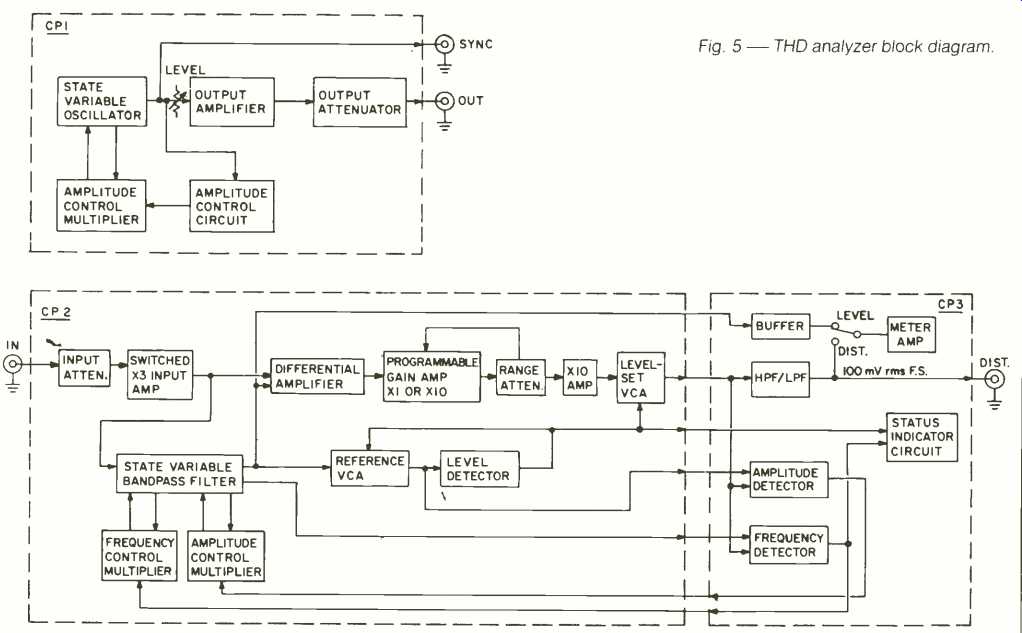
Fig. 5--THD analyzer block diagram.
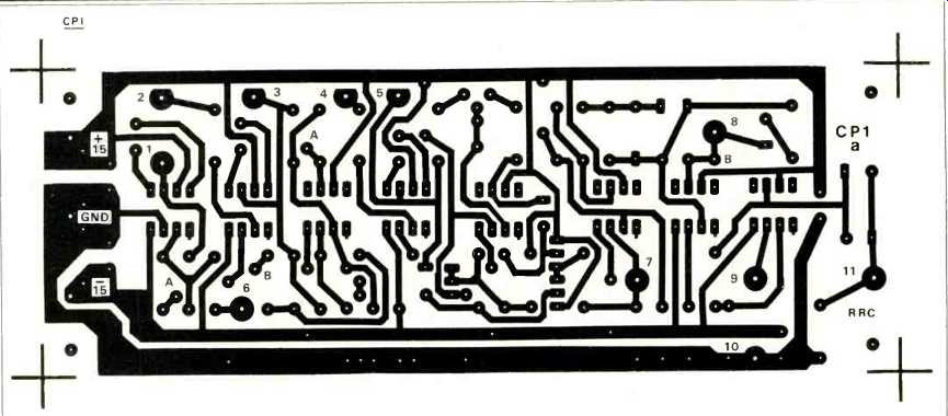
Fig. 10--Printed wiring board layout for CP1, the signal source.
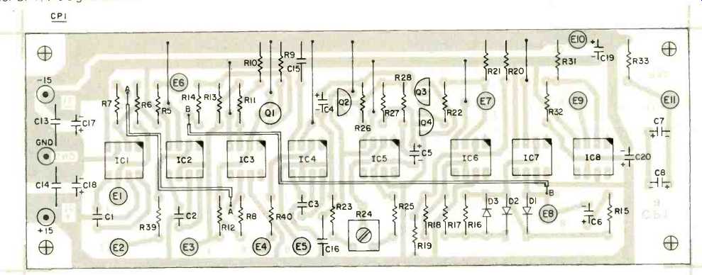
Fig. 11--Parts placement for CP1, the signal source.
Control of the center frequency of the bandpass filter is quite simple. Recall from our earlier discussion that the center frequency of a state-variable band pass filter can be changed by simply adjusting the loop gain. In Fig. 12 this is accomplished by connecting a multiplier and series resistor (R65) around the inverter formed by IC13 to provide con trolled amounts of negative or positive feedback. When the multiplier provides a non-inverted characteristic, additional negative feedback is provided around the inverter, making its gain less than unity and consequently lowering the center frequency of the filter. The opposite action results when the multiplier provides an inverted characteristic. In this manner the gain of the inverter can be controlled over a ±3.2 percent range, resulting in a center frequency control range of ±1.6 percent.
The multiplier consists of FET 05 and 1014, and it is identical to the one used in the oscillator (Fig. 9, Part I). As in the oscillator, any distortion introduced by the control circuit must pass through two integrators before reaching the output (El 8), and is thus substantially reduced.
Amplitude control of the bandpass filter is a bit more subtle. Based on last month's discussion of the simple state-variable filter, one's first inclination is to change the gain of the filter by changing the amount of the "damping" feedback, here provided by R57 and R62. This will surely accomplish the desired control, but notice that in this case any distortion injected by the control circuit will be removed from the filter output by only one integrator. To minimize distortion, we would like to inject the amplitude control signal at the same advantageous point as the frequency control signal, i.e., at the input of inverter 1013. Fortunately, it turns out that a small amount of feed back (positive or negative) around the second integrator (1015) is equally effective in providing control of the gain as long as the perturbation is small, as it is here. The amplitude control multiplier, consisting of FET 06 and IC16, thus provides amplitude control feedback from the output of IC15 to the input of' inverter IC13. An amplitude control range of about 3.5 percent results.
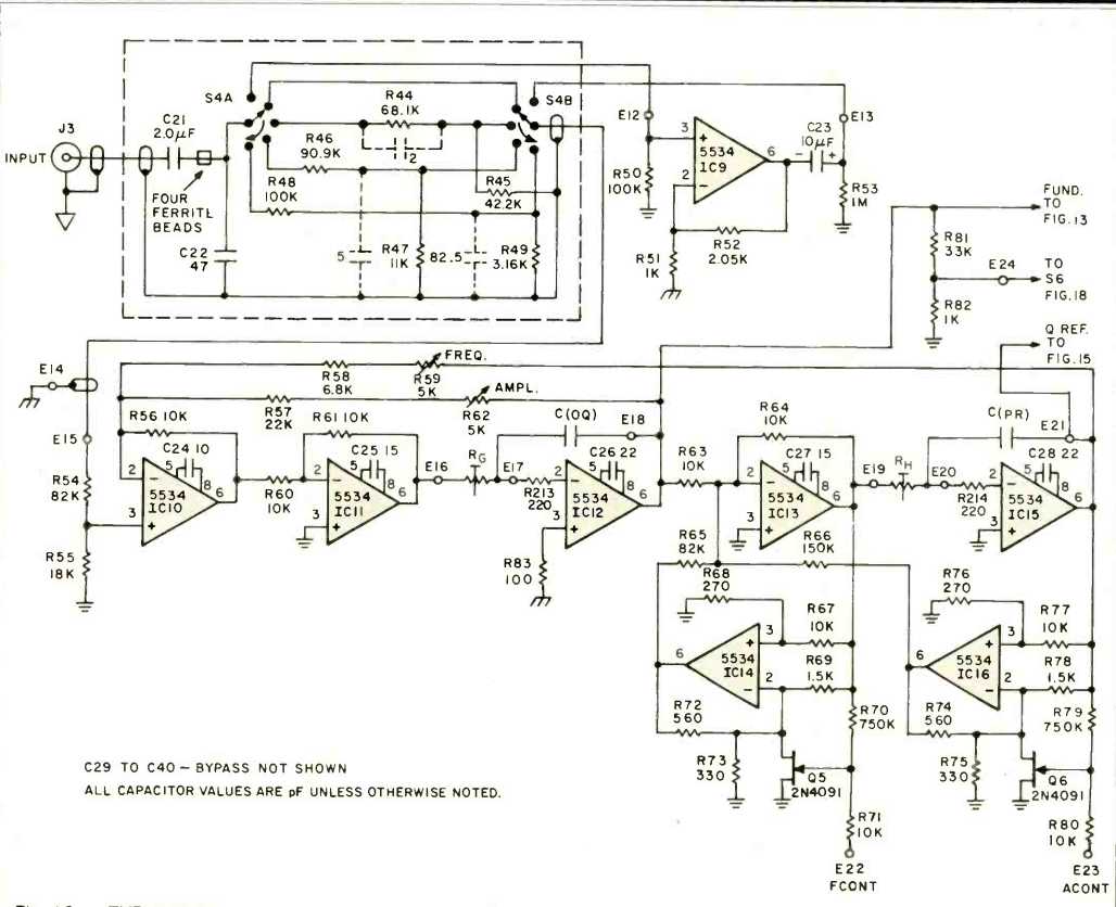
Fig. 12--THD analyzer voltage-controlled bandpass filter.
Differential and Product Amplifiers
The differential amplifier which completes the notch filter and the distortion product amplifiers are shown in Fig. 13.
Also shown here is the auto-set level circuit which will be discussed shortly.
1C17 functions as the differential amplifier where the fundamental supplied by the bandpass filter is subtracted from the input signal. The combination of this differential amplifier and the bandpass filter thus comprises the notch filter. The differential amplifier also provides a gain of 10 to the distortion products. The in put signal (E15) is applied directly to the high-impedance noninverting input of IC17 while the fundamental from the bandpass filter (El 8) is applied to the inverting input through R84. Because of the attenuation which results from the voltage divider formed by R84 and R85, nulling results when the fundamental' from the bandpass filter is about 10 percent larger than the fundamental sup--plied directly from the input attenuator.
The differential amplifier is followed by another amplifier (1C1 8) whose gain is 10 on all distortion ranges except the 10 percent and 3 percent full-scale ranges, where it is unity. The gain of this stage is switched by a FET whose gate voltage is controlled by the sensitivity switch (S5).
IC1 8 is followed by an attenuator which is also controlled by S5, establishing full scale sensitivities of 10, 3, 1, 0.3, 0.1 , 0.03, 0.01 , and 0.003 percent. This is followed by a fixed gain-of-ten amplifier (1019). The distortion product signal then proceeds to the auto-set level volt age-controlled amplifier (ICs 20 & 21).
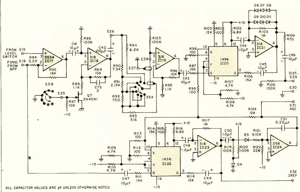
Fig. 13--THD analyzer product amplifier and level set.
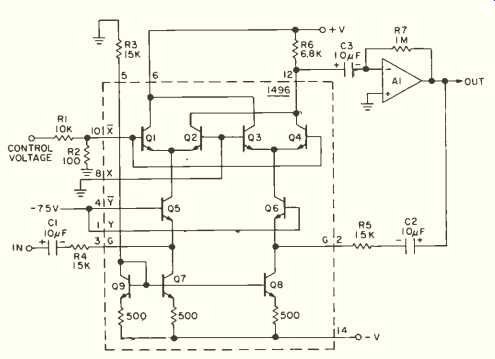
Fig. 14--A simple voltage-controlled amplifier (VCA).
Voltage-Controlled Amplifiers
Because the voltage-controlled amplifiers (VCA) are central to the operation of the auto-set level circuitry, we will discuss their operation before proceeding further.
A simple VCA is shown in Fig. 14. It consists of a 1496-type balanced modulator IC (whose internal circuit is shown) and an op-amp.
The op-amp is connected as an inverting feedback amplifier, the ratio of whose input and feedback signals is controlled by the 1496. As this ratio is varied from a very small number, through unity and on to a very large number, the gain changes proportionately from small to large. In fact, in this circuit the gain is numerically equal to the ratio. A d.c. control voltage applied to the 1496 controls this ratio and thus the gain.
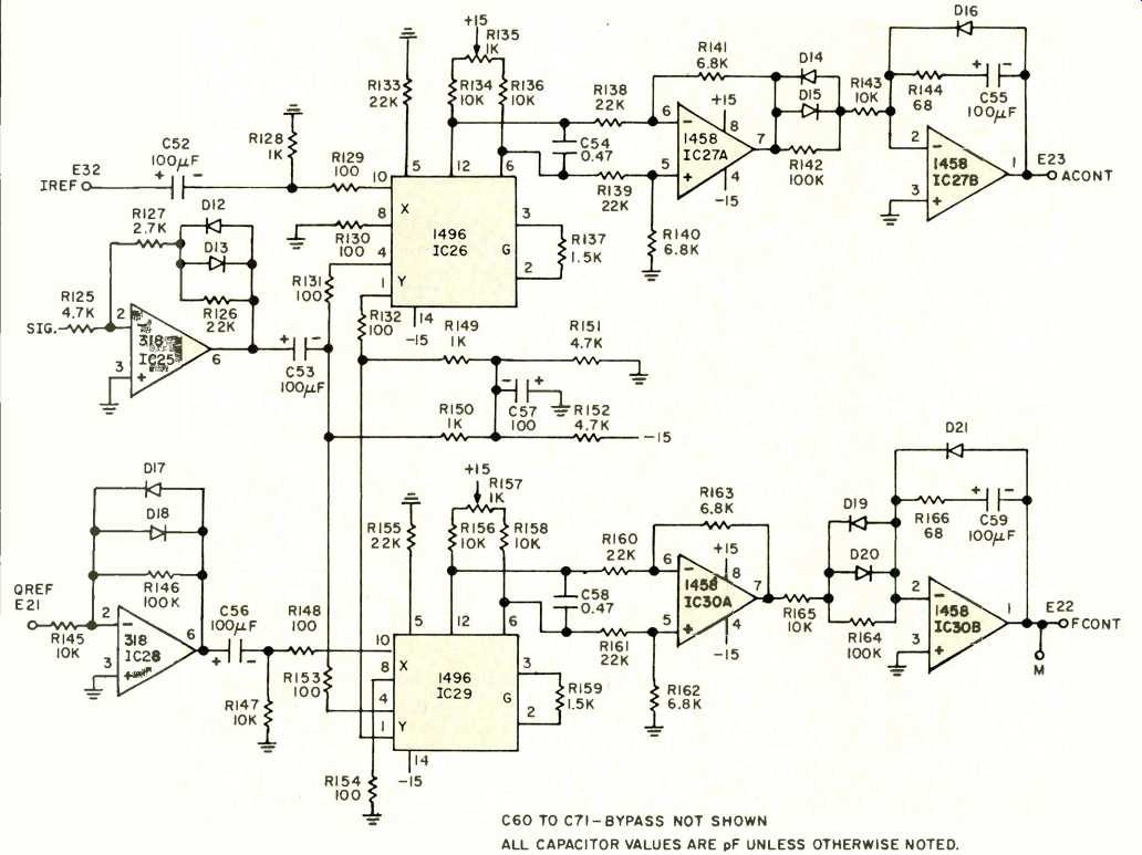
Fig. 15-THD analyzer amplitude and frequency detectors.
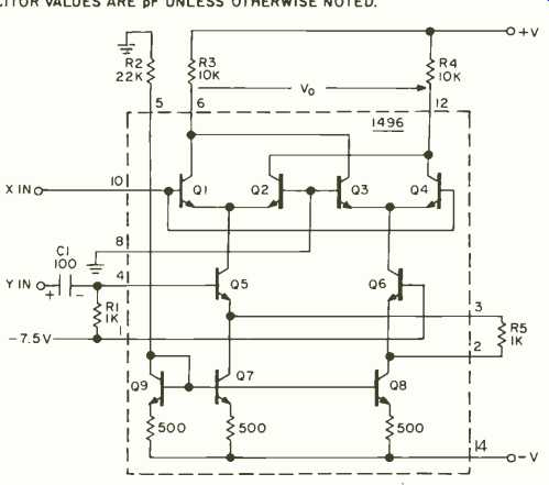
Fig. 16-A simple phase detector.
Referring to Fig. 14, bias resistor R3 sets up a bias current in 07 and Q8 of about 1 mA. Transistors Q5 and Q6 are connected as common-base stages and provide a low-impedance point at their emitters where a.c. signal currents can be added to the d.c. bias currents. The input signal current established by R4 is applied to the emitter of 05, while the feedback current established by R5 is applied to the emitter of 06. The action in the upper "quad" of transistors (01-04) determines what portion of each of these a.c. signals reaches the output at pin 12 and thus the inverting input of the operational amplifier.
We see that at the collector of 05 we have d.c. bias current plus a.c. input signal, while at the collector of 06 we have d.c. bias current plus a.c. feedback signal. Each of these currents is applied to the emitters of a differential pair, where some will flow in one emitter and the remainder will flow in the other emitter of a given pair. Each of these currents thus splits in some proportion. The key operating principle in this circuit is that the a.c. currents into the emitters of a differential pair will split in the same proportion as the d.c. bias currents flowing into the pair.
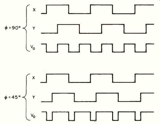
Fig. 17--Phase comparator operation.
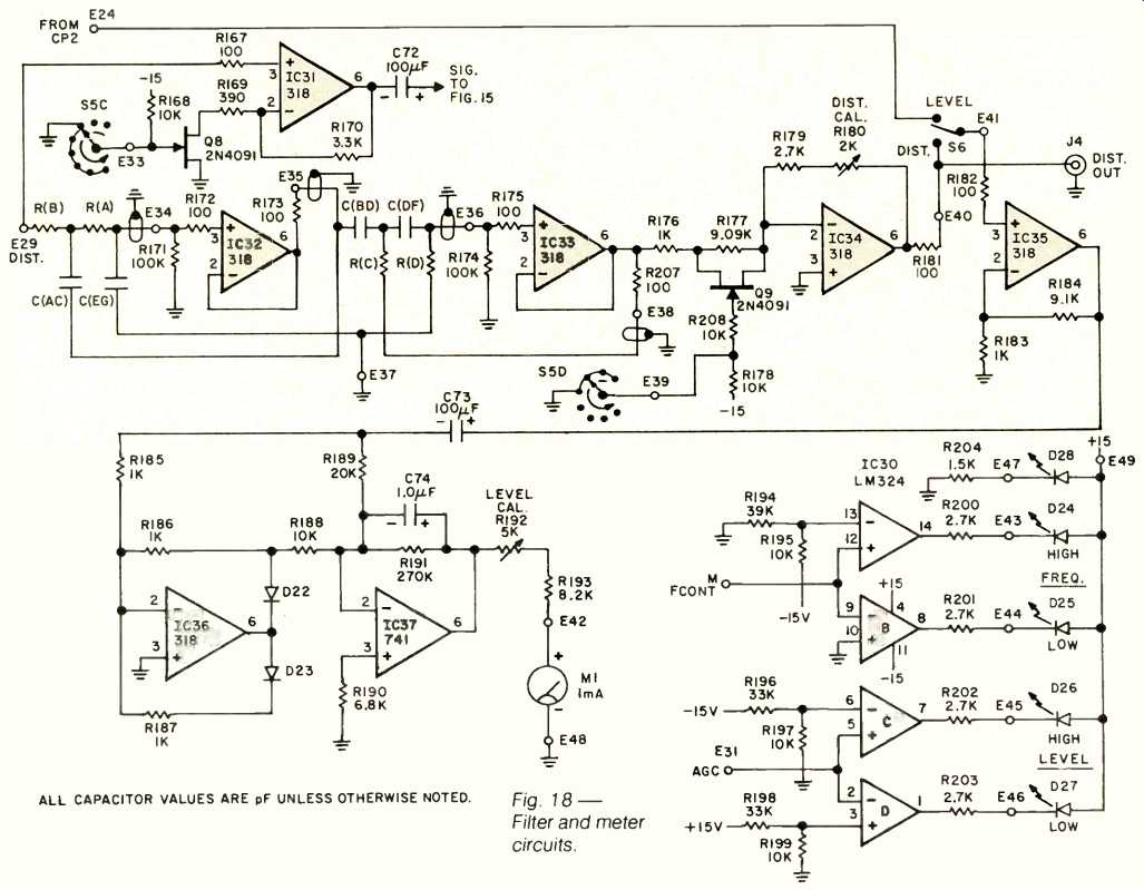
Fig. 18--Filter and meter circuits.
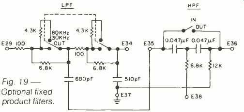
Fig. 19--Optional fixed product filters.
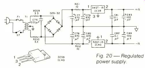
Fig. 20--Regulated power supply.
The attenuated control voltage applied to pin 10 controls this split. When the control voltage is zero, both transistors in each differential pair have the same base voltage and conduct equally.
In this case, half of the input signal and half of the feedback signal current reach the output at pin 1 2 via Q2 and Q4 respectively. Because of the extremely high gain of A1 , the signal and feedback currents at pin 12 must essentially cancel each other for finite output levels from A1 . They must therefore be virtually equal. This in turn indicates that the signal currents in R4 and R5 must be equal for a zero control voltage, implying unity gain.
A positive control voltage at pin 10 will cause Q1 and Q4 to conduct more heavily than Q2 and 03. Thus, a greater proportion of feedback current reaches pin 12 (via 04) than input current (via Q2). In order to maintain cancellation of the two currents at pin 12, the input signal must be larger to begin with than the feedback current, implying less than unity gain. As an example, it is well known that a potential of about 60 mV across the bases of a differential pair will cause a 10-to-1 ratio of conduction in the two transistors. In this application, a +60 mV control voltage at pin 10 will thus result in a gain of about 0.1. The situation is the inverse for a negative control voltage; a -60 mV level at pin 10 will result in a gain of about 10.
A particularly nice feature of this arrangement is that the gain in decibels is a linear function of the control voltage.
Here we get a variation of 20 dB/60 mV or about 0.33 dB per mV. The 100-to-1 attenuator formed by R1 and R2 simply allows for more manageable control voltages (3.3 dB per volt). The gain control range here is in excess of ±20 dB.
Auto-Set Level Circuit
With a knowledge of the operation of the VCA, the auto-set level circuit in Fig. 13 becomes easy to understand. It consists of two identical VCAs, each with the same control voltage and thus each with the same gain. The first VCA (1020, 21) controls the gain in the distortion product signal path and receives its in put from IC19. It produces the level-adjusted distortion product output at E29 for use on CP3. The second ("reference") VCA (1022, 23) controls the gain in an automatic gain control (a.g.c.) loop; its input is the filtered fundamental output from the bandpass filter (E18).
In addition to the reference VCA, the a.g.c. loop includes a level detector (D5) and an op-amp (IC24) connected as an integrator. The d.c. output of the integrator is the control voltage for the VCAs.
The a.g.c. circuit is arranged so that the integrator will always adjust the gain of the reference VCA so that the level of the fundamental at its output is 1.1 V rms.
Thus, if the input to the notch filter is the nominal 1-V level, the fundamental from the bandpass filter will be 1.1 V and the gain of both VCAs will be unity, as it should be for this situation. If the input signal level were to increase to 2 V, the gain of both VCAs would drop to 0.5, implementing the proper gain correction in the distortion product signal path.
Auto-Tune Control Circuits
The amplitude and frequency detectors which comprise the auto-tune control circuit are shown in Fig. 15. If the gain and center frequency of the band pass filter are not perfect, the notch filter will not produce a complete null of the fundamental signal. Some fundamental will thus appear in the distortion-product signal path. An amplitude error will produce a "left-over" fundamental component whose phase is zero (or 180) degrees relative to the input signal. A fundamental component with this phase relationship is said to be a "normal" component. A frequency error will produce a so-called "quadrature" fundamental component whose phase is either leading or lagging 90 degrees relative to the input signal.
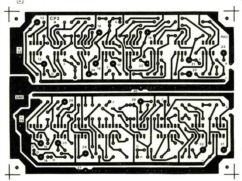
Fig. 21--Printed circuit board CP2 for the input circuit, bandpass filter, product amplifiers, and auto-set level circuits.
The amplitude detector functions by looking for normal fundamental components in the distortion signal and adjusting the bandpass filter gain up or down depending on the phase relationship (0 or 180 degrees). It ignores quadrature fundamental components. Similarly, the frequency detector functions by looking for quadrature fundamental components and adjusting the filter center frequency up or down depending on the phase relationship (lagging or leading). It ignores normal fundamental components.
The special detector circuit which possesses the properties mentioned above is called a "phase detector" be cause it is sensitive to the phase of the signal being detected. An ordinary envelope detector or rectifier is not suitable because it will detect the signal regard less of its phase. Here, the phase of the "left-over" fundamental is a crucial piece of information.
A simplified schematic of a phase detector is shown in Fig. 16. Like the VCA, it is based on the 1496-type balanced modulator IC. The phase detector is a more conventional use of this IC. Bias resistor R2 sets up an appropriate current flow in current sources Q7 and Q8.
The application of a positive input signal at the Y input will cause Q5 to conduct more current than Q6; the opposite will occur for a negative input signal. . A positive input at the X input will cause Q1 and Q4 to be "on" and Q2 and Q3 to be "off." The output (V0) is taken differentially between pins 6 and 12.
We can easily see what polarity of output will be produced for any combination of positive or negative X and Y inputs. For example, if X and Y are both positive, most of the current flow is in Q5 and--Q1, pulling pin 6 lower than pin 12 and producing a positive output. In general, a positive output is produced when both inputs have a like sign, and a negative output is produced when the X and Y inputs have differing signs. In a sense, this circuit performs similarly to the "EXCLUSIVE NOR" logic function. We immediately see that two perfectly in-phase signals at X and Y will always have the same sign and thus produce a maximum positive output.
The diagram in Fig. 17 lends further insight into the phase sensitivity of this type of detector. Square-wave inputs are shown for simplicity of illustration, but the circuit functions similarly for other waveforms. In the top illustration we see what happens when the X and Y inputs are 90 degrees out of phase; the aver age d.c. output at V. (which is what matters) is zero. This illustrates how the amplitude detector can ignore a quadrature component.
It is easy to see that if we slide the Y input back and forth along the time axis, an asymmetry will be produced in the Vo waveform, corresponding to an average d.c. value.
The bottom illustration depicts a 45-degree relationship between the X and Y inputs. By trigonometry we can argue that the Y signal consists of equal portions of normal and quadrature components in this case. This would be representative of a situation where there were both amplitude and frequency errors simultaneously. We see that in this case a positive average d.c. output is produced at V0. It is not, of course, quite as strongly positive as when X and Y are perfectly in phase.
We can see that if we apply an "unknown" signal to the Y input and a "reference" signal to the X input, the detector will respond to components in the un known signal whose phase is similar to (or the inverse of) that of the reference.
Components in quadrature with the reference will be ignored. In addition, the effects of noise and signals at other frequencies will average out to zero.
Returning to Fig. 15, the amplitude detector consists of ICs 25-27. The distortion product signal ("unknown") is taken from the output of 1031 (Fig. 18) and passes through IC25 where it sees a small-signal gain of five and is soft-limited beginning at ±0.7 V swings by the feedback diodes. The signal is then applied to the Y input of 1c26 where it is phase-compared with a "normal" fundamental provided by the output of the reference VCA (1c23).
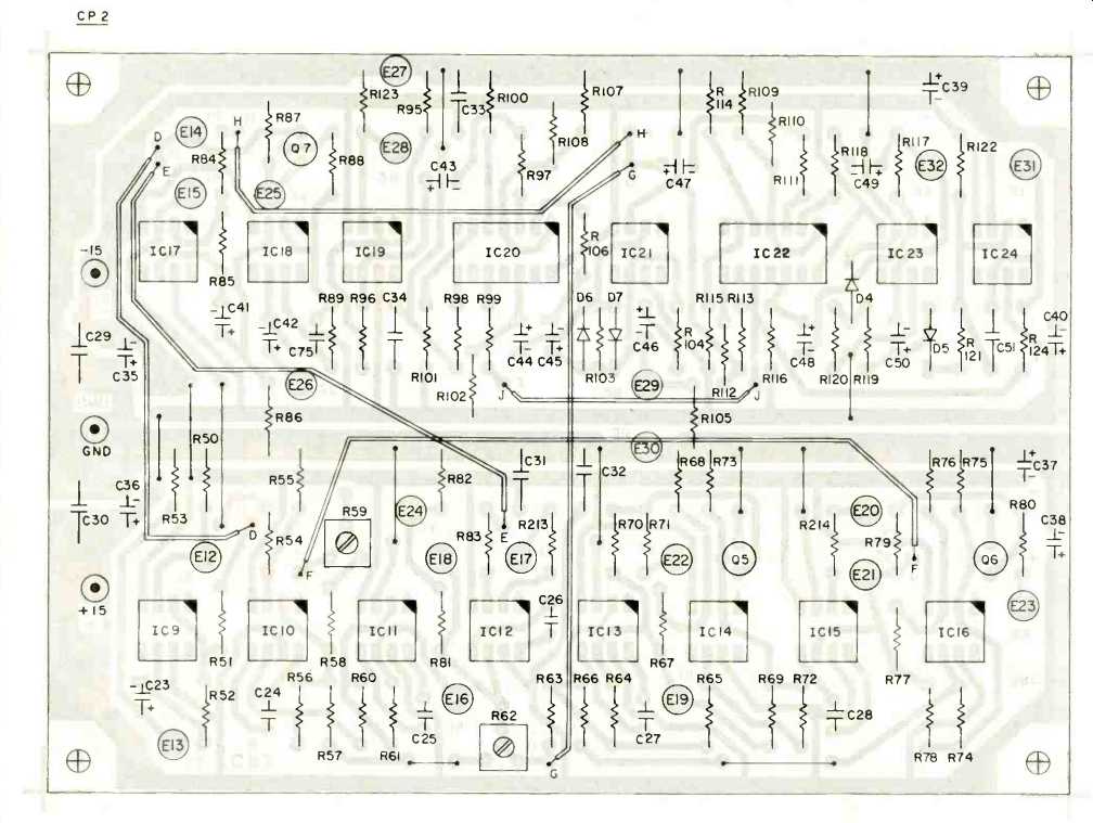
Fig. 22--Component placement for CP2.
The differential output of the phase detector is filtered and applied to IC27A where it is converted to a single-ended signal. This signal drives the integrator (IC27B) to produce the appropriate gate voltage for the amplitude control FET (Q6). The integrator will continue to ad just the gate voltage until the output of IC27A is driven to zero. Notice that when the error from IC27A is greater than ±0.7 V, D14 and D15 conduct and speed up the integrator to achieve faster tuning following a transient.
Operation of the frequency detector (ICs 28-30) is identical to that of the amplitude detector except that it is supplied with a quadrature fundamental reference (lagging 90 degrees) instead of a normal fundamental reference. The quadrature reference is supplied from the low-pass output (IC15) of the state-variable filter and passed through amplifier-limiter IC28 before application to the X input of IC29.
Filter and Meter Circuits
The filtering, metering, and status indicator circuits are shown in Fig. 18. The distortion product signal from the auto-set level VCA on CP2 (E29) is first amplified by a factor of one or 10 in 1C31 to keep it at a reasonable level for use by the auto-tune circuits for all sensitivity settings of S5. Switch S5C sets the gain of this stage to 10 on the 0.03-through 10-percent sensitivity ranges to compensate for attenuation introduced by the S5A attenuator on these ranges. Note that S5C does not affect gain in the distortion metering path.
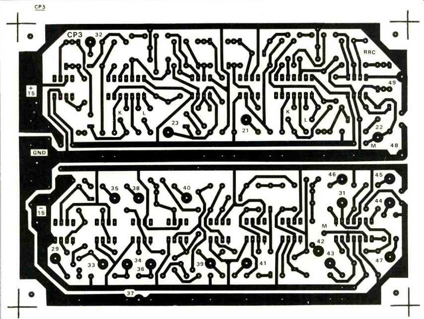
Fig. 23--Printed circuit board CP3 for the auto tune control, product filter, meter and status indicator circuits.
The distortion product signal from E29 is also applied to the low-pass product filter. As mentioned earlier, the second-order Bessel low-pass product filter is set for a 3-dB cutoff frequency equal to 10 times the fundamental frequency.
The filter consists of a pair of resistors (on S3), a pair of capacitors (on S1) and an op-amp (1032) connected as a volt age follower [3]. This filter is followed by the second-order high-pass filter (IC33) which is similarly realized. Its filter O is chosen to provide a slight gain bump at the second harmonic frequency to partly offset the small loss in the notch filter at this frequency. For reasons of high-frequency filter stability, the high-pass filter has the same set of cutoff frequencies on the 200-kHz range as on the 20-kHz range.
As mentioned in Part I, the tracking product filters add a considerable portion of the switching complexity and expense (about $25.00) to the analyzer.
Many professional analyzers provide only a switchable 400-Hz high-pass filter and a low-pass filter which can be set to 30 or 80 kHz or switched out. This simpler filtering approach can be implemented as shown in Fig. 19 with a SPST switch for the high-pass and a center-off DPDT switch for the low-pass. Use of this simpler filtering will typically result in an increase of the analyzer's residual by 0 to 3 dB and will make the reading somewhat more susceptible to hum and noise in the UUT.
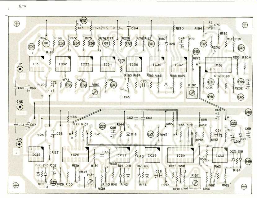
Fig. 24--Component placement for CP3.
Following the filters, the distortion product signal is brought to a 100-mV full-scale level by the switched-gain amplifier composed of FET Q9 and IC34.
The total gain of this combination is either 0.33 or 3.3 depending on the setting of S5D. Trimmer R180 provides calibration for the distortion measurement.
Provision is also made to monitor the input level with the meter circuits. This makes it possible to make a complete THD measurement on a piece of equipment without any other test instruments.
Selection of distortion or level as the quantity to be measured is accomplished by S6. In the "Level" position, an attenuated output from the bandpass filter is applied to the meter circuits. The full-scale "Level" range then corresponds to the setting of the input attenuator. Note that this provides a narrowband measurement of the input signal level.
The distortion product signal is then applied to the meter circuit, consisting of IC36 and IC37. IC36 is connected as a unity-gain inverting feedback amplifier which has two feedback paths, one for positive output-signal excursions (D23) and one for negative output excursions (D22). Positive and negative half-wave rectified signals thus appear at the two feedback resistors. The negative half-
wave rectified signal and half the unrectified input signal are added at the input of IC37 to produce a full-wave rectified result. This amplifier also provides appropriate low-pass filtering of the result. The single-ended output of IC37 is then used to drive the meter movement.
The status indicator circuits indicate whether the incoming level is too high or too low for proper analyzer operation, and whether the incoming frequency is too high or too low for the auto tune circuits. A quad op-amp comparator (IC38) drives the four indicator LEDs.
The frequency indicator circuit monitors the gate voltage on the frequency control FET (05) to see if the frequency is within the tuning range. If the gate volt age is zero or positive, the frequency is too low, and the "Low" LED is lit. If the voltage is more negative than-12 V, the FET is pinched off and the frequency is too high.
The input level indicator circuit monitors the a.g.c. control voltage in the auto-set level circuit. If this voltage goes more negative than -3.5 V, indicating that the input level is more than 11.5 dB above the nominal 1-V internal operating level, the "High" LED will be lit. Similarly, a level more than 11.5 dB below the nominal operating level will light the "Low" LED.
Power Supply
The regulated ±15 V power supply for the analyzer is shown in Fig. 20. The circuit employs a full-wave bridge rectifier and standard three-terminal regulator ICs.
The input circuit, bandpass filter, product amplifiers and auto-set level circuits are realized on printed circuit board CP2. Its layout is shown in Fig. 21 and the component placement diagram is shown in Fig. 22. The auto tune control, product filter, meter and status indicator circuits are realized on CP3. Its layout is shown in Fig. 23, while component placement is illustrated in Fig. 24.
This completes the description of all of the circuitry in the THD analyzer. Next month, below, we'll conclude with construction details, the adjustment procedure, troubleshooting, and performance data.
------------
Part 3:
by ROBERT R. CORDELL
In Parts I and II the theory and operation of all of the THD analyzer circuits were covered. We will now proceed with construction, adjustment, and troubleshooting. It goes without saying that a thorough understanding of Parts I and II will help immensely in troubleshooting.
Circuit Board Assembly
Assembly of the three printed wiring boards should be quite straightforward if the component placement diagrams are followed carefully. Load all of the IC sockets first (socketing is strongly recommended); this will make it easier to identify locations of other components.
Note that pin #1 of all ICs faces in the same direction except for IC38. Next load the off-board connection terminals ("E" connections denoted by large do nut lands on p.c. cards), including those for the power-supply leads. Any suitable terminals may be used here, but Vector Type T-18 terminals are a good choice.
The boards come drilled with 0.042-inch holes at these locations for maximum flexibility, but will have to be re-drilled to 1/16-inch for the T-18 terminals.
Now load all resistors, diodes, bare jumpers, capacitors, transistors, and insulated jumpers--in that order. Take special care to watch polarity on diodes and polarized capacitors. An elongated pad on the p.c. card denotes the negative terminal of most capacitors and the cathode of all diodes. Also take special care in reading the color code on carbon resistors and the resistance code on precision resistors; many different codes exist for the latter. If you have any doubt, use an ohmmeter. Note that the two diode strings on CP2 (D6-8, 9-11) are each prewired and treated as a single component. Prior to installing FETs Q1, Q5, and 06, it is a good idea to measure and record their pinch-off voltage (V0) with the simple circuit of Fig. 24. Knowledge of the pinch-off voltage will permit the best adjustments to be made. Use of 22-gauge, insulated, solid wire is OK for the long insulated jumpers. Note that each of these jumpers connects two points on the board labeled with the same letter of the alphabet.
Complete circuit board assembly by installing all ICs in their sockets, taking care to avoid bent pins, which can sometimes be hard to detect. Again, note that pin #1 of all ICs faces in the same direction except for IC38.
Circuit Board Bench Test
Because this is a fairly complex construction project which also involves considerable chassis wiring, it is strongly recommended that most of the electrical testing, troubleshooting and adjustment of the three circuit boards be done one at a time on the bench. This will virtually guarantee success upon final assembly.
Before proceeding further, give each of the boards a thorough visual inspection, checking for incorrect polarities or values, cold solder joints, solder bridges or other shorts, improper IC insertion or placement, missing components or jumpers, etc. This step should not be bypassed.
A ±15V regulated power supply will be required for bench testing. If you don't have one, you may wish to assemble the analyzer's power supply module now and use it.
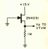
Fig 24--Test circuit for measuring J FET pinch-off voltage.
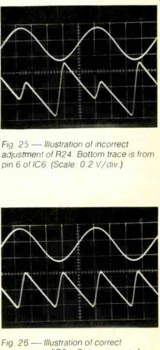
Fig. 25--Illustration of incorrect adjustment of R24. Bottom trace is from pin 6 of IC6. (Scale: 0.2 V/div.)
Fig. 26--Illustration of correct adjustment of R24. Bottom trace is from pin 6 of 106. (Scale: 0.2 V/div.)
Signal Source
Prepare CP1 for bench testing by soldering 0.022-µF, ± 10% polyester capacitors from terminal E2 to E3 and from E4 to E5. Connect 3.9-kilohm resistors from E1 to E2 and from E3 to E4. Connect a 2.7-klohm resistor from E5 to E6. Strap E5 to E9. Connect a 0.1-µF polyester capacitor from E7 to ground. Center the trimmer pot. Connect ± 1 5V to the power supply terminals (observe polarity!). Connect a scope to E5.
If all is well, you should see 4.5V p-p sinusoid at about 2 kHz on the scope. In any case, it is wise at this point to check all important d.c. voltages. Table 1 provides a listing of all key d.c. voltages as actually measured in the prototype. "BQ3" means the base of Q3, GQ1 means the gate of C1,-IC1 means the inverting input of IC1, OIC1 means the output of 101,101-6 means pin 6 of 101, etc. Values indicated by an asterisk may depend on the input signal, adjustment or something similar, and they may not be close to those listed under certain conditions. All values assume a steady state condition. A voltmeter with a 1 megohm or greater input impedance should be used. Be very careful to avoid shorting adjacent pins on ICs when probing (especially pin 6 on the 318s). When possible, clip to a resistor connected to the desired point instead. When probing certain sensitive points (like the inverting input of an op-amp), it may be necessary to isolate the meter probe with a 10-kilohm resistor to pre vent high-frequency oscillations.
A check of the key voltages for CP1 should reveal any problems at this point and aid in finding the cause. It is worth noting that the inverting and non-inverting inputs of an op-amp properly operating with negative feedback should never differ by more than a few millivolts. If a greater difference is observed, there are three possibilities: First, the stage may be over-driven by the input, which may point to trouble further back in the chain.
The second is a bad (or unpowered) op-amp. This is generally the case if the polarity of the input differential is lot consistent with the output polarity. It this occurs, the output of the op-amp is usually saturated near one power supply rail. If the output is zero, a short from output to ground may be present. The third possibility is a fault in the associated input or feedback circuitry. In this case, the polarity of the input differential will be consistent with the output polarity. In any case, troubleshooting complex circuits involving many possible interactions re quires care, thought, arid patience. The key lies in separating cause and effect.
Often a particular portion of the circuit can be made to look faulty by a problem elsewhere.
If the signal at E5 is large and clipped, and the gate voltage of Q1 is strongly negative, the fault is probably associated with the multiplier circuit (IC3). If the gate voltage is about +0.5V, the problem lies with the a.g c. control circuit (IC6,7) or the a.g.c. detector (Q2-Q4). In this case a large positive level (greater than +2.5V) at E7 points to the 106.7 circuitry. A low level (less than 1 V) points to the detector circuitry.
If the signal at E5 is zero and the gate voltage of 01 is strongly negative, the problem lies with the 106.7 circuitry. If the gate voltage of Q1 is about +0.5V, something is wrong with the oscillator proper (101,2,4).
An unstable or varying level indicates a problem with the IC6,7 circuitry involving a.g.c. loop stability. Check R21, R15, R16, R17, C6 and the capacitor connected to E7.
Now check the main output at E1 1. It should be three times as great as that at E5 if the output amplifier is operating properly.
Replace the resistors from E1 to E2 and E3 to E4 with 39-kilohm resistors.
The frequency should drop to about 200 Hz. Observe the full-wave rectifier sawtooth waveform at pin 6 of IC6.
Make sure the signal is full-wave and not half-wave; the latter indicates trouble involving IC5, Q3 or Q 4. Adjust R24 for perfect symmetry, i.e., so that adjacent peaks are of equal level. Incorrect and correct adjustments of R24 are illustrated by the 'scope photos in Figs. 25 and 26.
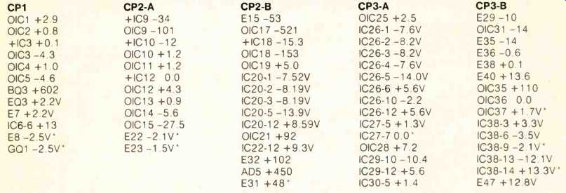
----- Table 1--Key d.c. voltages as measured in completed prototype analyzer operating at 1 kHz with 1V rms input on the 3V input range, reading 0.0005°° distortion on the 0.003°° sensitivity range. All voltages are in millivolts unless otherwise noted.
The asterisk (' ) denotes voltages which depend strongly on operating conditions, FET pinch-off voltages, etc. Keep in mind that many voltages may depend significantly on op-amp input offset voltage or bias current, and may even have the opposite sign in some cases.
Replace the capacitors at C(KM) and C(LN) with 0.22 µF, ±10% polyester capacitors. Connect a 1.0-µF polyester capacitor from E7 to ground. The frequency should now be about 20 Hz, the level should be the same as before, and a stable level should be realized within 15 seconds after power is applied.
Input Amplifier And Bandpass Filters (CP2)
Prepare CP2 for bench testing by connecting 0.022-µF, ±10% polyester capacitors from El 7 to El 8 and E20 to E21. Connect 3.9-kilohm resistors from E16 to E17 and E19 to E20. Ground E14, E15, E22 and E23. Connect ± 15V to the supply terminals, carefully observing polarity.
Check all d.c. voltages for this circuitry (Fig. 12) in Table 1. Pay less attention to those with asterisks. If problems are found, they should be corrected now.
Apply 1V rms at 2 kHz to E12 and check for a 3V rms output at E13. Apply the same signal to the bandpass filter input at E15. Observe the signal at E18. It should exhibit a bandpass characteristic centered at about 2 kHz as the input frequency is varied. Set the frequency for maximum output. Adjust R62 for a level of 1.15V rms at E18. Adjust R59 for a center frequency of 2 kHz and re-trim R62.
Observe the signal at pin 6 of IC14. It should be approximately 1.0V p-p and in-phase with that at E19. Temporarily remove the short from E22 to ground and connect E22 to -15V. The signal at pin 6 should now be about 1.0V p-p and inverted from that at E19. Repeat this procedure for pin 6 of IC16 with phase checked relative to that of E21 and changing the voltage on E23 from ground to -15V. The results should be about the same. If either of these procedures reveals a problem, one of the multipliers (IC14, Q5 or IC16, 06) should be suspected. Note that changing the volt age on E22 should slightly affect the center frequency (about ±1.6%), while changing that on E23 should only slightly affect the amplitude at E18 (about ± 3.5%). Check for about 30mV rms at E24.
Product Amplifiers And Auto-Set Level Circuits (CP2)
Connect a 10-kilohm resistor from E27 to E28 and an 82-kilohm resistor from E26 to E28, and check the d.c. voltages for this circuitry (Fig. 13) in Table 1. Voltage measurements at the pins of IC20 and IC22 should be made through a 10-kilohm isolating resistor at the end of the meter probe to prevent oscillations.
With the 1V rms, 2-kHz signal still applied to Et 5, sweep the frequency and observe the output at E26. A notch should be observed at the center frequency of the bandpass filter. Try to ad just the generator frequency and the set ting of R62 for a deep notch (less than 10mV rms). If R62 doesn't have enough range, connect E23 to -15V instead of ground and try again. Now offset the generator frequency to obtain a 100mV rms output at E26. Ground E25 and ob serve a level of 1.0V rms at E26. remove the ground at E25. Check pin 6 of 1019 for a level of 100mV rms.
Now check the auto-set level circuitry.
A level of about 1.1V rms should appear at the output of the reference VCA (E32), independent of input level over a ±10-dB range. At the nominal 1V rms input level, E31 should be at about OV d.c., while plus and minus 10-dB input levels should result in approximately minus and plus 3V respectively at E31. Recovery to nominal output from a 20-dB drop in input level should take about 10 seconds.
If the level is too large and E31 is strongly negative, the circuitry associated with IC22 and IC23 is probably faulty. If E31 is strongly positive, the circuitry associated with D5 and 1024 should be suspected. If the level is too low, the opposite polarities at E31 will point to the problem areas above.
Check the distortion product output at E29. A level of 100mV rms should be observed, independent of input level variations over a ±10-dB range about 1V rms. This assumes that there is still 100mV rms at pin 6 of 1019 when the input level is 1V rms.
Auto-Tune Circuits (CP3)
Prepare this portion of CP3 (including 1031, Fig. 18) for bench testing by connecting a 10-kilohm resistor from E29 to ground. Center trimmers R135 and R157. Connect ±15V to the supply terminals of CP3 (observing polarity) and check the relevant voltages in Table 1. Voltage measurements to the pins of 1026 and IC29 should be made through a 10-kilohm isolating resistor. By offset ting R135 or R157, it should be possible to get the respective integrator outputs at E23 and E22 to drift slowly in a positive or negative direction between approximately -12V and +0.3V.
Apply 100mVrmsat 2 kHz to E29 and observe the same signal at pin 6 of 1031. Observe a somewhat softly clipped 1.5V p-p version of the signal at pin 6 of 1025. Briefly short E33 to ground and observe a 1V rms level at pin 6 of 1031 and a 2.5V p-p rounded square wave at pin 6 of 1025. Apply 100mV rms at 2 kHz to E21 and ob serve a softly clipped 0.8V p-p level at pin 6 of 1028. Increase the input level to 1V rms and observe .3 hard clipped 1.0V p-p signal at pin 6 of C28.
Further bench testing of CP3 requires the use of CP2. If any problems remain on CP2, correct them now before proceeding. Prepare CP3 by making inter connections E21, E29 and E32 from CP2 to CP3. Remove the existing connections at E22 and E23 on CP2 and make interconnections E22 and E23 from CP3 to CP2. Center R135 and R157. It is assumed that E25 is open and that the attenuator between E26 and E28 is still in place.
With the 1V rms, approximately 2-kHz signal applied at E15 as previously, check pin 6 of 1025 for a 3V p-p rounded square wave. If the level is very small, the analyzer may have tuned it self. In this case, changing the frequency by about 10% so that it is well out of the tuning range should yield the square wave. Also check for a 1V p-p square wave at pin 6 of IC28.
Adjust the input frequency for a mini mal output at E29 and measure the d.c. voltage at E22. Set the input frequency to yield a voltage equal to one-half the pinch-off voltage measured for 05 (3.5V if you didn't measure it). Now adjust R62 for a d.c. voltage equal to one-half the pinch-off voltage of 06 at E23. A complete null of the fundamental should now be present at E29, with only distortion and noise visible.
Now place a 100-to-1 attenuator between E29 on CP2 and E29 on CP3; a 100-kilohm series resistor and a 1-kil ohm shunt resistor to ground will do. Alternately adjust R135 and R157 for the best possible fundamental null as ob served at E29 on CP2. These adjustments should be made slowly, as the time constants in the auto-tune control circuits are long.
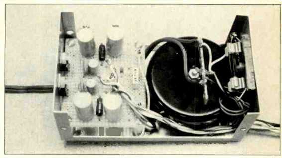
Fig. 27--Interior of the ±1 5V power supply module. A toroidal power transformer was utilized in the prototype to minimize hum.
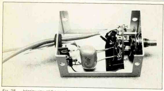
Fig. 28--Interior view of the input attenuator module.
Filter. Meter And Status Circuits
Strap E35 to E36 and E40 to E41.
Connect a 10-kilohm resistor from E34 to ground. Connect a 1-kilohm shunt resistor from E42 to ground. Center R180 and R192. Apply power and check the relevant voltages in Table 1.
Apply a 300mV rms, 2-kHz signal to E34. Check for 300mV rms levels at pin 6 of ICs 32 and 33. Adjust R180 for about 100mV rms at pin 6 of 1034 and 1V rms at pin 6 of 1035. Drop the input level at E34 to 30mV rms and short E39 to ground. Observe about 100mV rms at pin 6 of 1034 and 1V rms at pin 6 of IC35. Check for 1.4V p-p half-wave rectified signals at the anode of D22 (negative-going) and the cathode of D23 (positive-going). Check for a positive d.c. level of about 1.1V at E42.
Remove the strap from E40 to E41 and place a strap from E24 on CP2 to E41. Apply a 3V rms, 2-kHz signal to El 5 on CP2 and check for 1V rms at pin 6 of IC35. Adjust R192 for a +1.1V d.c. level at E42.
Check the status circuits by connecting our LEDs from terminals E43 through E46 to +15V. Remove the strap from E24 to E41 and replace the strap from E40 to E41. Reconnect E29 on CP2 directly to E29 on CP3. Connect a 1V rms 2-kHz signal to E15 on CP2.
D26 and D27 should be extinguished, while D24 or D25 should light if the input frequency is tuned above or below the tuning range respectively. They should both be extinguished if a good notch is being observed at E29. Drop the input level to 0.25V rms; D27 should light.
Raise the input level to 4V rms; D26 should light.
Bench testing of the circuit boards is now complete. If any problems surface after final assembly, they are probably not on the circuit boards.
Chassis Assembly
The first step in chassis assembly is to build the power supply module. It is built inside a 2 1/4 by 3 by 5 1/4 inch aluminum utility box. This affords some shielding against 60-Hz hum. Conventional point to-point wiring is used, employing a perforated board for component mounting.
The voltage regulator ICs should be bolted to one wall of the enclosure and insulated with mica washers. Make sure that metal burrs don't cause shorts between the enclosure and the ICs. The power supply module is bolted to the rear of the analyzer enclosure, with the line cord passing through both the power supply and the notched-out analyzer cover.
Power leads and switch wiring pass to the interior of the analyzer through a grommet in the power-supply enclosure.
A polarized line cord is recommended to guarantee that the power switch is al ways on the neutral side of the a.c. line so as to minimize hum. The power transformer should be mounted in the module so that it is at the extreme right-rear of the analyzer, far away from CP1 and CP2. A photograph of the power supply is shown in Fig. 27.
Although the choice of the power transformer is not critical, use of a toroidal design (as shown) will assure low induced hum. The Avel-Lindberg 40/ 3004 used here is available from Sager Electrical Supply Co., 60 Research Rd., Hingham, Mass., 02043 at a cost of about $24.00. In any case, the input voltage to the regulators under the full analyzer load should not be less than 18V (including ripple dips) nor greater than 35V. If necessary, adjust R21 1 and R212. The 40/3004 transformer does not have much extra current capacity, so be particularly observant of regulator headroom in this case.
The three circuit boards should De mounted on %-inch threaded 6-32 standoffs and placed as shown in Fig. 4 (Part I, July issue). CP1 is placed so that IC1 is closest to the front panel. CP2 is placed so that IC9 is closest to the front panel. CP3 is placed so that IC38 is closest to the front panel. Make all of tie power-supply connections and then the connections between CP2 and CP3. Circuit board power and ground should be distributed on a single-point basis from a terminal strip mounted near the input jack (J3).
Two types of shielded cable were used in this project, low-capacitance microphone cable (34pF/ft.) and high-capacitance miniature cable (124pF /ft.).
Unless specified, the miniature cable can be used. Use a shielded cable for the E29 interconnection (shield grounded only at E30).
Now mount and interconnect all of the remaining front panel items except the range and frequency switches (S1 and S3). The resistors residing on the output level, input level, and sensitivity switches (S2, S4 and S5) should be wired onto the switches prior to mounting of the switches.
Level control R30 should be connected to E9 through a shielded cable. The shield should connect to El 0 and the CCW end of R30. The output attenuator (S2) should receive its ground directly from the single-point ground. R205 will ultimately be suspended between S2C and S11.
As mentioned earlier, the input attenuator should be mounted in a small, shielded enclosure as shown in Fig. 28.
Use shielded cable from the input jack and single-point ground to the attenuator. Four ferrite beads are placed on the lead from C21 to S4 for improved r.f immunity. Connect the output of the attenuator to E15 on CP2 with low-capacitance shielded cable. Note that the shield supplies ground to the secondary single-point ground (E14) on CP2.
Selection of the attenuator frequency compensation capacitors (shown dotted in Fig. 12) will require experimentation, as the required values and even topology (series vs. shunt connection) will depend on particular parasitics. The best approach is to do the compensation be fore installing the module, using the actual required length of low-capacitance cable at the output looking into a 100 kilohm low-capacitance load (or a 100 kilohm, 100-to-1 resistive attenuator).
Use an audio generator and an audio a.c. voltmeter or oscilloscope to achieve a flat frequency response on all ranges with the module's cover in place.
High-capacitance shielded cable is recommended for connection of the sensitivity switch (S5A) to E28. Note that the attenuator receives its ground from E27 via the shield. The "hot" ends of R90 and R94 on S5A can be connected to a nearby unused switch position.
If you have chosen to implement the simple fixed-product filters of Fig. 19 in stead of the tracking filters, wire them now. Use shielded cable for the connections to E29 (on CP2), E34, E35, E36 and E38. The filter ground connection should come via the shield of the cable going to E34, which shield can be connected at E37. The shield of the cable going to E29 should be connected only at E30 on CP2. The 510-pF capacitor in Fig. 19 should be made smaller by the amount of the cable capacitance in parallel with it.
Intermediate Check-Out At this point, prior to the wiring of the range and frequency switches, a moderately thorough check-out of the analyzer is recommended. This can be done if the temporary tuning capacitors and resistors installed for bench testing have been left on the boards. We assume here that the capacitors in place are 0.022 µF and that the resistors are 3.9 kilohm. The 0.1-µF capacitor from E7 to ground and the 2.7-kilohm resistor from E5 to E6 on CP1 should also be in place. If you have chosen to implement the tracking product filters, strap E29 to E34 and E35 to E36. Connect the source output (J2) to the analyzer input (J3).
The analyzer can now be put through a full set of paces at 2 kHz. Note that you may have to adjust R59 and per haps R62 to get a run and have reason able FET control voltages at E22 and E23 (say,-1 to-4V). Also check the oscillator a.g.c. FET gate voltage at E8.
Check all functions of the analyzer under a variety of level and sensitivity conditions to determine that everything is working properly. Look for evidence of oscillations.
"Distortion" from a separate signal generator can be injected through a 62 kilohm resistor into the connection between the source and the analyzer. If the source is producing 1V rms and the separate signal generator is delivering 100mV rms to the resistor, a 0.1 % "distortion" level will result. Check the calibration of R180 and R192. Check for satisfactory tuning time and instrument residual. If any problems are uncovered, correct them now.
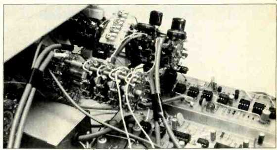
Fig. 29—Close-up of the specially constructed range and frequency switches.
Final Assembly
Assembly of the range and frequency switches may require some ingenuity.
S1 consists of nice five-position, two-pole wafers if the tracking product filters are implemented. The resulting length will usually require that S1 be assembled with parts from two or more rotary switches. The shat can be extended by sawing off the shaft from a second switch and affixing it to the shaft of the switch under construction with a standard shaft couple. The pair of 4-40 screws which hold the switch together can be extended by joining additional lengths of 4-40 screw to them (obtained from the second switch) with tapped 4-40 standoffs. A close-up of the switches assembled in this way is shown in Fig. 29. Alternately, the Centralab switch components specified in the parts list can be assembled into the required switch.
The capacitors are mounted between adjacent wafers as shown in Table 2.
For example, C(KM)-1 mounts between poles K and M at position 1. Poles S1 A and S1 B are on the wafer closest to the front panel. The capacitor and resistor designations for switch-mounted components assume that the tracking product filters are being implemented and that their components are mounted on the switch sections closest to the front pan el. Note that the tuning capacitors for the highest frequency range have a small resistor in series with them. This resistor compensates for a high-frequency phenomenon in active filters known as "0-enhancement" which results from op-amp high-frequency rolloffs. These resistors can be mounted on the unused position-5 switch terminals. Note that the tuning capacitors are wired so that there is always some capacitance connected even when the switch is between positions, preventing undesirable transients.
This is accomplished by wiring the position-4 terminals in parallel with their respective wipers. The use of shorting-type switches would also have accomplished the transient suppression.
The high-pass product filter capacitors [C(BD) and C(DF)] for the 20-kHz range are also used for the 200-kHz range by connecting positions 3 and 4 of the associated switch poles together.
This was done because stability of higher frequency active high-pass filters would have been a problem, and the additional filtering is not really necessary on the highest range.
As shown in Fig. 29, the four frequency trimmers (R1 to R4) were mounted on a small piece of perforated board and mounted to poles J and H of S1 with 18-gauge solid bare wire. R206 is mounted on the switch between the two wipers.
After S1 is assembled and loaded with components, mount it and make all possible interconnections to the circuit boards. Each of the four tuning capacitors [C(KM), C(LN), C(0Q) and C(PR)] is connected to the circuit boards by seven inches of low-capacitance shielded cable. The capacitance of the shielded cable is directly in parallel with that of the associated tuning capacitor. Instead of being grounded, the shield interconnects one side of the tuning capacitor to the output of the associated integrator.
Thus, for example, the shield connects one side of C(KM) to E3. The capacitance of this length of cable has been taken into account in the values of the tuning capacitors for the 200-kHz range, and appropriate alterations should be made to these capacitors if other values of shielded cable capacitance are used.
The shields are connected to switch poles K, L, 0, and R.
Frequency switch S3 consists of eight 11-position, single-pole wafers, and should be constructed in the same way as S1 above. If possible, it is recommended that switch shields be installed between sections 4 and 5 and between sections 6 and 7. The resistors on S3 are mounted between adjacent positions on a given wafer. The wiring is documented in Table 3. For example, R(A) 12 goes on S3A, the wafer closest to the front panel, between positions 1 and 2.
Although precision 1% resistors are preferred for R(E) through R (H), the only requirement is that the four resistors of each position be matched to each other within 1%. Thus, you may save some money or hassle by measuring and matching 5% carbon-film resistors. If you buy 10 of a given value at the same time, there is a very good chance you'll find four with the required match. Try not to get all of the resistors which err on the high side placed on one wafer, and vice versa.
As with the tuning capacitors, S3 is wired so that resistance is present even when the switch is between positions.
This is done by wiring the position-1 terminal to the switch wiper. The free end of the lowest valued resistor connected to position 11 can be tied to position 12 if you have a 12-position switch or to a small, insulated terminal on or near the switch if you have an 11-position switch.
With S3 assembled and loaded with components, mount it and make all of the remaining interconnections. Where possible, make the interconnections with positions on S1 that already have a wire running back to the appropriate circuit board terminal.
Connection of the tracking-filter components on S1 and S3 to E29, E34, E35, E36, E37 and E38 can be done with shielded cables as discussed earlier for the fixed filtering option. In this case, however, the connections to E34 and E36 must be made with low-capacitance shielded cable. The value shown for C(EG) for the 200-kHz range assumes about eight inches of this cable. The product filter interconnections between 51 and S3 need not be shielded, but should be dressed as far away as possible (i.e., against the front panel) from the signal leads and components of the oscillator and analyzer sections. There is a very substantial amount of gain between the oscillator/BPF circuits and the product filters. Failure to get adequate isolation here could result in oscillations, particularly on the 200-kHz range. Leads associated with the analyzer section should also be dressed away from those of the oscillator section. Assembly of the analyzer is now complete.
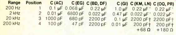
Table 2--Capacitor connections on range switch S1. The asterisk (' ) indicates polypropylene. polycarbonate or polyester of at least 100 V working voltage. The dagger (j') indicates polystyrene or silvered mica, again of at least 100 V working volt age. The others are not critical.
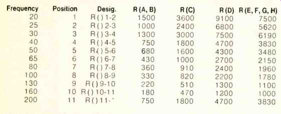
Table 3--Resistor connections on the frequency switch S3. The asterisk indicates a tie-point. position 12 if available; otherwise use an insulated terminal. R (E. F. G. H) should be 100. 1/4-watt carbon-film types where each group of four like values should be matched to within 1%. Others are standard 5%, 1/4-watt carbon film. All values are shown in ohms.
Test and Calibration
The signal source should be checked first. Center trimmers R1 to R4. Apply power, and monitor the main output on a 'scope and a.c. voltmeter. Also monitor the d.c. voltage at E8, the gate bias for 01. Check operation at all frequencies.
Check frequency response flatness and level stabilization time. Check to see that the gate voltage of 01 does not get with in 0.5V of either zero or the measured pinchoff voltage at any frequency.
Check the action of the output attenuator and level control. If you have a frequency counter, check all the frequencies; at this point they should be within ±20% of the selected value, and should increase monotonically as the frequency switch is advanced. Check for oscillations as well.
Set the analyzer to 650Hz, and adjust frequency trimmer R2 for a source frequency of exactly 6E0Hz if you have a frequency counter. Otherwise use a Lissajous pattern with a 650-Hz oscillator as a reference. Connect the signal source to the analyzer input, and apply 1V rms on the 3V input range. Monitor the d.c. levels at E22 (frequency control) and E23 (amplitude control). Adjust R59 and R62 as necessary to get the analyzer to tune and to set these voltages to half the measured pinchoff voltages of the associated FETs.
The remaining frequency trimmers in the oscillator will now be adjusted to bring the oscillator into alignment with the center frequency of the analyzer for the remaining frequency ranges. At 65Hz, adjust R1 so teat the d.c. voltage at E22 equals half the recorded pinchoff voltage for 05. Adjust R3 at 6.5 kHz and R4 at 65 kHz in the same manner. Now check the voltages at E22 and E23 at all frequencies to make sure that neither one gets within 0.5V of either zero or the associated pinchoff voltage. Make com promise adjustments among R1, R3, R4, R59, and R62 as appropriate. A problem with the E22 voltage (frequency control) may mean an incorrect frequency-setting resistor somewhere on S3.
Now that the oscillator trimmers are set, it would be useful to recheck the oscillator frequency calibration. Typically it should be within ±10%.
If the amplitude control voltage (E23) changes substantially toward the high end of the frequency range (between 50 kHz and 200 kHz), this could be an indication that the Q-enhancement compensator resistors in series with C(OQ) and C(PR) on the highest range need some adjustment. The value shown in the schematics is a goat compromise value, but it does depend somewhat on the individual rolloff characteristics of the op-amps (ICs 10, 11, 12, 13, and 15). If E23 goes too positive (toward zero), these resistors may be too large. If E23 goes too negative, these resistors may be too small.
Another phenomenon to watch for toward the high end of the 200-kHz range is "slewing oscillations." Too much phase lag around an active-filter loop can cause 0-enhancement and, ultimately, oscillation. if the signal being handled by an active filter causes one or more of the op-amps to slew-rate limit, the effect is equivalent to a substantially increased phase lag. This can result in oscillations which drive the amplifiers even deeper into slew-rate limiting. The only way to stop such an oscillation is to tune to a lower frequency or remove power. The normal signal levels in this analyzer cannot touch off such an oscillation, but a sufficiently large transient can. That is why the range and frequency switches are wired so as not to generate transients when they are operated.
However, occasionally a power-on transient can trigger such an oscillation in this analyzer if it is powered up when tuned to greater than about 100kHz.
The frequency response of the tracking product filters should be checked at this point by injecting a signal at their input in place of E29. If the level at three times the front-panel setting is taken as 0 dB, then the lower and upper 3-dB-down frequencies should be at 1.4 and 10 times the set frequency, respectively (0.1 4 and about 8 times on the 200-kHz range).
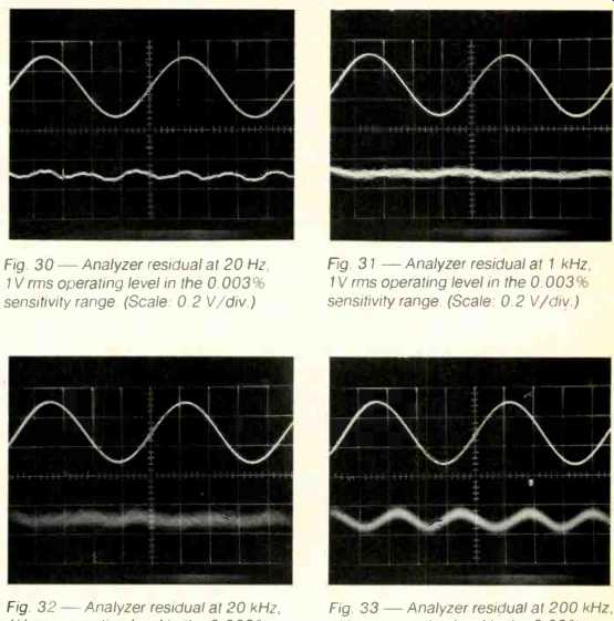
Fig. 30--Analyzer residual at 20 Hz. 1V rms operating level in the 0.003% sensitivity range. (Scale: 0.2 V/div.)
Fig 31- Analyzer residual at 1 kHz. 1V rms operating level in the 0.003% sensitivity range. (Scale: 0.2 V/diy.)
Fig. 32--Analyzer residual at 20 kHz. 1V rms operating level in the 0.003% sensitivity range. (Scale: 0.2 V/div.)
Fig. 33--Analyzer residual at 200 kHz. 1V rms operating level in the 0.03% sensitivity range. (Scale: 0.2 V/div.)
To calibrate the distortion reading, two signal sources should be used. Apply 1V rms at 1 kHz to the analyzer from the internal signal source. Put S6 in the "Level" position and adjust R192 for a full-scale reading with the input attenuator on the 1V range. Apply 1V rms at 3 kHz from a second audio generator through a 62-kilohm resistor. The analyzer will now see 0.99V at 1 kHz and 10.1 mV at 3 kHz, or a "distortion" level of 1.02%. Set the sensitivity switch (S5) to the 1% range and adjust R180 for a meter reading just a hair over full-scale.
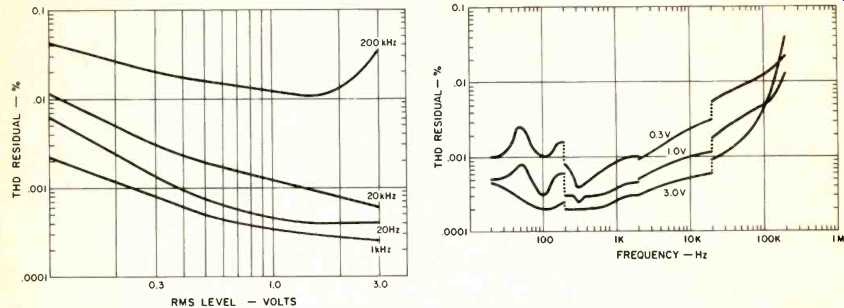
Fig. 34--Residual vs. level as a function of frequency in the 3V input range.
Fig. 35--Residual vs. frequency as a function of input level in the 3V input range.
To complete testing, measure the analyzer's residual at all frequencies and at various levels by connecting the signal source directly to the analyzer input. it is useful to observe the "Dist. Out" signal on a 'scope at this point.
If the residual seems particularly noisy or jumpy on only one range, don't hesitate to suspect the trimmer pots and the tuning capacitors. This is a sensitive application and even minor deficiencies in these components may cause trouble; I've experienced trouble with both. I strongly recommend the use of high-quality tuning capacitors.
Hum can be particularly insidious in an instrument such as this where full scale sensitivities on the order of 30 microvolts are encountered. Although the construction details are intended to minimize hum, you may still have to fight it. It will be most noticeable on the 200-Hz range. Remember, hum can be picked up capacitively by a high-impedance circuit (shielding helps here) or it can be magnetically induced into any circuit, including grounds. Hum will probably be reduced when the instrument is fully housed in its enclosure.
Performance
Performance of the prototype is illustrated in Figs. 30 to 35. Scope photos of the analyzer's residual at the nominal 1V internal operating level for 20 Hz, 1 kHz, 20 kHz, and 200 kHz are shown in Figs. 30 to 33.
The total residual (noise and distortion components) is plotted as a function of level for the four frequencies above in Fig. 34. The residual as a function of frequency for 0.3,-1.0 and 3.0V rms internal operating levels is plotted in Fig. 35. Best performance is generally achieved near the high end of its allow able range of operating levels. At operating levels above about 1.5V rms, the residual is below 0.001% across the full audio band.
Parts Availability
A serious attempt was made to de sign the THD analyzer with readily avail able parts, and many constructors will have no trouble finding most of the parts at normal outlets. As an aid, however, several dealers of various parts are listed below. Because of the substantial number of parts involved in this project, I recommend obtaining and searching through the catalogs that many of these and other companies make available. Al though most of these companies provide broad lines, a few are worth special mention because they have some of the less commonly available parts. The NE5534AN op-amps and the Centralab rotary switches are available from New ark Electronics ($25.00 minimum order).
The 2N4091 J-FETs and a suitable power transformer are available from CFR Associates. Precision one-percent resistors are available from International Electronics Unlimited.
Digi-Key Corp. P.O. Box 677 Thief River Falls, Minn. 56701 800/346-5144
Active Electronic Sales Corp. P.O. Box 1035 Framingham, Mass. 01701 617/879-0077 CFR Associates, Inc.
Newton, N.H. 03858 Jameco Electronics 1355 Shoreway Rd.
Belmont, Calif. 94002 415/592-8097
Newark Electronics 146 Route 1 Edison, N.J. 08817 201/572-2103 (or contact nearest branch)
International Electronics Unlimited 435 First St., Suite 19 Solvang, Calif. 93463 805/688-2747
PARTS LIST
All resistors are 1/4-watt, 5-percent carbon-film unless otherwise specified. Those specified as "1 percent" a-e 1/4-watt metal-film types. Substitution of 5-percent resistors for the 1-percent type will only degrade accuracy of the attenuators.
R1, R2, R3, R4, R59, R52, R192-5 kilohm trimpot (Panasonic K4A53) R5. R19, R58, R102, 81 16, R140, R141, R162, R163, R190-5.8 kilohm R6, RI I, R14, R15, R18, R22, R23, R26, R27, R56, R60, R61, R63, R25, R64, R67. R71, R77, R8C, R87, R96, R134, R136, R143, R145, 3147, R156, R158.
R165, R168, R178, R188, R195, R197, R199, R208-10 kilohm R7, R66-150 kilohm R8, R72, R74-560 oh m R9, R73, R75-330 ohm R10. R68, R76-270 kilohm R12, R69, R78, R137, R204-1 5 kilohm R13, R70, R79-750 kilohm R16. R33, R50, R86, 8105, R119, R120, R123, R142, RI46, RI64, RI71, R174 100 kilohm R17, R31, R82, R128, R149, R150, R183, R186, R187-1 kilohm R20, R35-I 3 kilohm R21, R41. R42, R43. R53. R103. R117-1 megohm R24, R135, R157-1 kilohm trimpot (Panasonic K4A13) R28, R57, R126, R133, R138, R139, R155, R160, RI61, R206-?2 kilohm R29-5.6 kilohm R30-2.5 kilohm potentiometer R32, R84-2.2 kilohm R34-2.0 kilohm R36-1.8 kilohm R37-820 ohm R38-620 ohm R39, R40, R213, R214-220 ohm R44-68.1 kilohm, 1 percent R45-42.2 kilohm, 1 percent R46-90.9 kilohm, 1 percent R47-11 kilohm, 1 percent R48-100 kilohm, 1 percent R49-3.16 kilohm, 1 percent R51, R176-1 kilohm, percent R52-2.05 kilohm, 1 percent R54, R65-82 kilohm R55. R85-18 kilohm R81, R196. R 198-33 kilohm R83, R98, R99, R101, R1I2, R113, R115, R129, R130, R131, R132, R148, R153, R154, R167, R172, R173, R175, R181, R182, R207-100 ohm R88-I.1 kilohm, 1 percent R89-10 kilohm, 1 percent R90-7 5 kilohm, 1 percent R91-2 15 kilohm. 1 percent R92-750 ohm, 1 percent R93-316 ohm, 1 percent R94-6.2 kilohm R95-1.1 kilohm R97, R100, R106, R111, R1 14, R118-15 kilohm R104-470 ohm R107, R108, R109, R110, R125, R151, R152-4.7 kilohm R121-910 kilohm R122-22 megohm R124-12 kilohm R127, R179, R200, R201, R202, R203 2,7 kilohm R144, R166-68 ohm R169-390 ohm R170-3 3 kilohm R177-9.09 kilohm, 1 percent R180-2 kilohm trimpot (Panasonic K4A23) R184-9.1 kilohm R189-20 kilohm R191-270 kilohm R193-8.2 kilohm R194-39 kilohm R205-2.7 megohm R209, R210-3.3 ohm, 2-watt; remove if using 40/3004 transformer R21 1, 212-10 ohm, 2-watt; see text R(A) through R(H)-See Table 3 and text C1, C25, C27-15 pF silver mica (Arco DM15-150) C2, C3, C26, C28-22 pF silver mica (Arco DM15-220) C4. C5, C23, C4I , C43, C45, C46, C47, C49-10µF, 25-V radial electrolytic (Panasonic ECE-AIEV100S).
C6, C7, C8, C17, C18, C35, C36, C42, C52, C53, C55, C56, C57, C59, C66, C67, C72, C73, C83, C84-100 µF, 16-V radial electrolytic (Panasonic ECE AICV101S) C9-1 µF, 100-or 250-V metallized polyester (Panasonic ECO-E2105KZS) C10-0.47 µF, 100-V metallized polyester (Plessey Minibox 0.47/100 F box) C11-0.1 µF, 100-V metallized polyester (Plessey Minibox 0.1/100 C box) C12, C76-0.01 µF, >100-V metallized polyester (Plessey Minibox 0.01/630 C box) C13, C14, C15, C16, C29, C30, C31, C32, C33, C34, C60, C61, C62, C63, C64, C65, C81, C82-0.1 µF. 25-V ceramic disc (Panasonic ECK-DIE104ZFZ) C19, C20, C37, C38, C39, C40, C44, C48, C50, C68, C69, C70, C71, C74-1 µF, 50 V radial electrolytic (Panasonic ECE-AIHVO 10S) C21-2 µF or 2.2 µF, 250-V metalized polyester (Panasonic ECQ-E2225KZS) C22--47 pF silver mica (Arco DM15-470) C24--10 pF silver mica (Arco DM15-100) C51--0.22 IF, 100-V metallized polyester (Plessey Minibox 0.22/100 D box) C54, C58--0.47 µF, 50-V (Radio Shack 272-1071) C77, C78, C79, C80--470 µF, 35-V radial electrolytic (Panasonic ECE-AIVV471S) C (AC) through C (PR)--See Table 2 and text D1 through D23--Switching diode (1N914, 1 N4 ' 48 or equiv.) D24 through D28--Red LED (Opto Electronics XC209R) D29 through D32--1N4002, 1N4003, 1 N4004 or equiv. 01, 05, 06, 07, 08, 09--2N4091 J-FET (National) Q2, Q3, Q4--2N3904 or equiv. gen. purpose silicon; NPN ICI, IC2, IC3, IC4, IC8, IC9, IC10, IC11, IC12. IC13, IC14, IC15, IC16, IC17-NE5534AN (Signetics, TI) 105, IC6, IC7, IC18, IC19, IC23, 1C25, IC28, IC31, IC32, IC33, IC34, IC35, 1C36-LM318N (National, TI, etc.) IC20, IC22, IC26, IC29--LM1496N (National, Mot., etc.) IC24--LF356N (National, Fairchild, etc.) IC27, IC30-LM1458N (National, Mot.) IC37-UA741CN (Fairchild, National, etc.) IC38--LM324N (National, etc.) IC39-LM3407-15 or UA7815CT (Nation al, Fairchild) IC40-LM3207-15 or UA79I 5CU (Nation al, Fairchild) Ti--32-48 V c.t., 1-amp power transformer (e.g., CFR Associates Tranny 1 or Avel-Lindberg 40/3004) Fl--'-A 3AG slow-blow fuse S1--5-position, 9-section, 18-pole rotary switch (Centralab PA302 6-inch index assy., Newark #22F652 plus 9 PA-32 sections, Newark 422F842 or see text). (If using fixed filters, 5-position, 6-section, 12-pole, PA1 033, Newark #22F833) S2--5-position, 2-section, 4-pole rotary switch (Centralab PA1013, Newark u22F813) S3--11-position, 8-section, 8-pole rotary switch :Centralab PA302 6-inch index assy., Newark #22F652 plus 8 PA-30 sections, Newark #22F840 or see text). (If using fixed filters, 11-position, 4-section, 4-pole, PA1015, Newark #22F815) S4--5-position, 1-section, 2-pole rotary switch (Centralab PA1003, Newark #22F803) S5--11-position, 4-sect on, 4-pole rotary switch (Centralab PAI 015, Newark
#22F815) S6--Miniature SPDT switch S7--Miniature SPST switch M1--1-mA meter movement, preferably with 0-' and 0-3 scales (MURA PM-702) Misc.--case; power supply and input attenuator enclosures; line cord; BNC jacks; knobs; shielded cable; PWB terminals; DIP sockets; mounting hardware, etc. A set of three etched, drilled and solder-plated circuit boards (CP1, CP2 and CP3) is available for $35.20 post-paid (in continental U.S.A.) from Circuit-Works, 1118 7th Ave., Neptune, N.J. 07753. New Jersey residents must add 5-percent sales tax. Please allow 3 to 4 weeks for delivery.
(adapted from Audio magazine, 1981)
= = = =
Also see:
Measuring Speaker Motion With A Laser--PART TWO (Sept. 1981)
KEF 105 Series II Loudspeaker (Feb. 1982)
The Roots of High Fidelity Sound (June 1981)