MANUFACTURER'S SPECIFICATIONS
Power Output: 200 watts per channel, both channels driven into 8 ohms, with less than 0.1% total harmonic distortion or intermodulation distortion, from 20 Hz to 15 kHz; 251 watts per channel, both channels driven into 4 ohms, with less than 0.25% total harmonic distortion or intermodulation distortion, from 20 Hz to 15 kHz; 501 watts mono mode with less than 0.25% total harmonic distortion or inter modulation distortion from 20 Hz to 15 kHz. Signal-to-Noise Ratio: 110 dB. Damping Factor: 500.
Dimensions: 19 in. W x 7 in. H x 12 in. D.
Weight: 49 lbs.
Price: $839.00
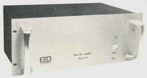
The BGW 500D, yet another addition to the 20 to 30 stereo power amps in the 150 to 200 watt per channel power class, appears to be quite well made, about as solid as a brick. The basic chassis is a rectangular steel box with the top open.
The power transformer is appropriately large and is mounted on the inside left (as viewed from the front). An L-shaped bracket is attached to the internal floor of the chassis and has mounted to it two 10,000 uF/75V capacitors, a diode bridge rectifier, a silicon controlled rectifier, and a three-terminal barrier strip to terminate the incoming line cord. Two large power resistors are mounted on the bottom of the chassis; one is in series with the a.c. line to reduce inrush current and gets relay shorted after a short time delay, and the other is in series with the SCR which is wired across the plus and minus terminals of the power supply.
On the inside rear of the enclosure is a barrier strip for primary strapping of the power transformer, the cooling fan, and a PC board containing the turn-off time delay and the SCR crowbar control circuitry.
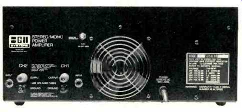
Fig. 1-Rear panel.
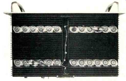
Fig. 2-Interior view.
Covering the top of the enclosure (except for about an inch in the middle) are the two heat sink/amplifier modules.
These are large sinks with two rows of six TO-3 power transistors mounted on them. On the non-fin side of the sinks are the amplifier circuit boards. Connections are made to the power supply's input and output through an 11-pin connector mounted on the circuit board. Over the top of the heat sinks is the top cover of the unit, which is solid on the top and rear and open at the left and right ends. The arrangement is such that the air flow from the fan comes up between the heat sinks in the middle and is forced to travel horizontally through the fins to the exit ports in the top cover. All in all, a very effective cooling scheme.
The front panel, which is 3/16-in. thick, has two beefy handles, a rocker-type power switch/circuit breaker, and a LED power-on indicator. On the rear panel are two pairs of five-way binding post speaker connectors, two phone-jack input connectors, the power cord, and a protruding 1/4-in. shaft that operates the stereo/mono switch.
Circuit Description
The first stages of the 500D are those of a LM318 operational amplifier. The output of the op amp feeds a complementary pre-driver stage, Q1 and Q2, operating at a collector current of about 25 mA. Considerable emitter degeneration is present in this stage, which raises the output impedance, giving the output stage more of a current source, improves stage linearity, and helps the stage quiescent current stability.
Connected between the collectors of Q1 and Q2 is the bias shunt regulator, Q3. The output stage is a quasi-complementary emitter-follower. Q4 and Q6 are Darlington connected followers, driving the composite pus half-cycle output transistor, consisting of Q8, 10, 12, 14 and 16 in parallel. Q5 is the input to the compound-connected minus half cycle side of the output stage. Q7 is an emitter-follower, driving the minus half-cycle composite-output transistor, Q 9, 11, 13, 15, 17 in parallel. Q6 and Q7 drivers are RCA multiple-emitter-site devices, and all outputs are RCA single diffused types.
Negative feedback is taken back in two loops. One loop, via R9 and C9, is around the predriver and output stage, and the overall loop, through R5 and C3, is around the total amplifier.
Mono full-bridge operation of this unit is selected by pushing in the shaft on the rear panel. A switch on one amplifier's circuit board converts one channel to a unity gain inverting circuit with its input fed from the output of the other channel. The load is then taken between the hot terminals of each channel and effectively doubles the output voltage giving the per channel four-ohm power into a single eight-ohm load.
There is no instantaneous VI limiting in this circuit, adequate safe area being provided by the multiplicity of output devices. A circuit on the time-delay circuit board senses plus and minus d.c. levels in the output of each channel and if considered excessive, triggers the SCR crowbar device which shorts the plus and minus 75 V supply together through a two-ohm resistor. This discharge of the power supply causes the primary circuit breaker to open, thus shutting off the amplifier and protecting the load.
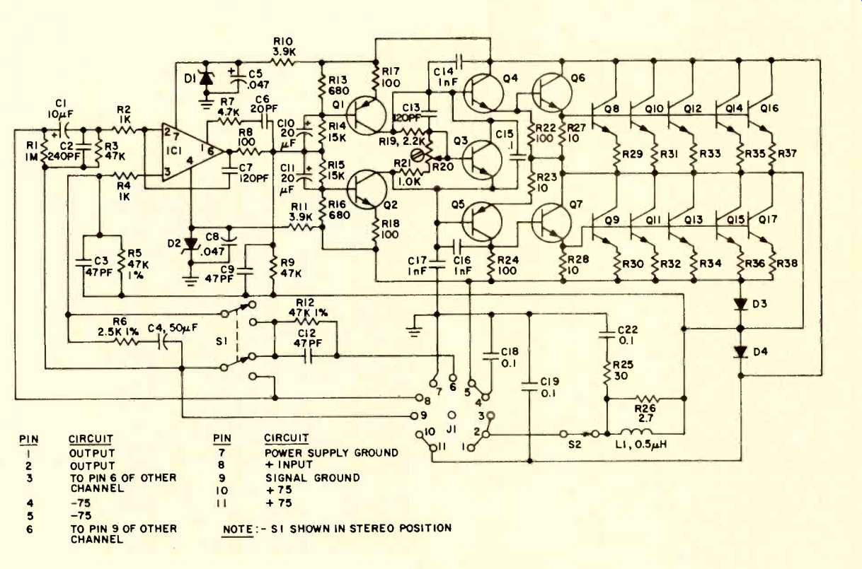
Fig. 3-Schematic of BGW 500D.
Listening Tests
The 500D was listened to on the reviewer's arrays and a pair of Dahlquist DQ-10s recently loaned to Audio for amplifier review purposes. The bass reproduction on this amplifier is excellent, giving good control of the DQ-10 woofers. It is relatively free of upper bass boominess and has good lower bass punch. The midrange sound is similarly good, though the high end sound has a bit of brightness or edginess.
Measurements
The 500D was first run at one third of rated power, 66.6 watts, into eight-ohm loads for one hour with a 1 kHz test frequency. Under these conditions, the fan alternately ran at low and high speed. The unit was then run for a second hour into four-ohm loads. Rated power into four ohms is 251 watts per channel and the test power was therefore 83.7 watts per channel. This time, the fan ran continuously at high speed and exhausted plenty of heat. Fan noise at high speed is fairly loud and could be objectionable to some people in a home music installation but would probably be okay in industrial and PA applications. However, if one is really pushing the amp hard and the fan does go to high speed, the resulting music level would in all probability drown out the fan noise. All things considered, this unit has excellent thermal capability and is one of the few units on the market that has adequate cooling for low impedance loads.
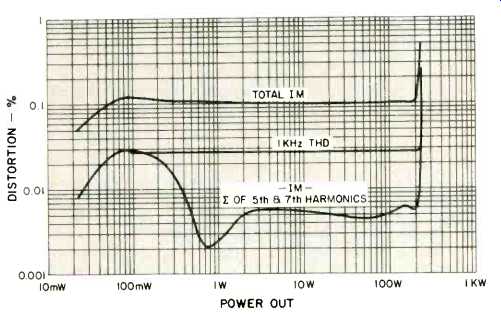
Fig. 4--Distortion versus power into 8-ohm loads.
Voltage gain was measured and found to be 20X or 26 dB, which is normal gain for power amps. IM distortion along with 1 kHz THD is shown in Fig.14. The measured behavior of this amp is different from any other thus far in that the IM and 1 kHz THD are virtually independent of power over a very wide range. The predominant harmonic distortion is even order, stemming from a gain imbalance per half cycle.
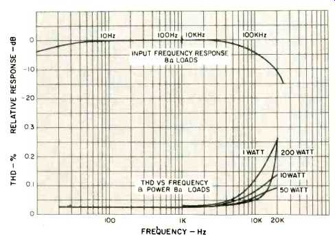
Fig. 5--Upper curve, 1-watt frequency response with 8-ohm loads (note break
in scale at 100 Hz-10 kHz); lower curve, THD versus frequency and power with
8-ohm loads.
It wasn't determined just where in the circuit that this gain imbalance occurred, but it could be in the way the unit is internally grounded and/or in the output stage where the minus half cycle or compound side has more gain than the cascaded emitter-followers in the plus half-cycle part of the circuit. The distortion products on IM are essentially a 60-Hz square wave which indicates even-order nonlinearity, and on THD, the residue looks like a full wave rectified sine wave, again indicative of even order nonlinearity. There are some higher order odd harmonics present also, mainly due to crossover distortion and are shown in Fig. 4. The fact that they peak at about 100 mW instead of disappearing below 1-10 watts, as has been characteristic of the better amps tested, may be partially responsible for the slightly harsher high end exhibited by this amp in the listening tests. The predominance of even-order products may be responsible for the apparent extra brightness observed.
Figure 5 illustrates the one-watt frequency response and THD vs frequency and power. The high end rolloff is at a lower frequency than usual, being 3-dB down at 80 kHz. The THD curves reveal increasing high frequency distortion with decreasing level. This is mainly caused by crossover or notch distortion where the magnitude starts to increase with frequency due to the falling compensated open-loop-gain characteristic. The magnitude of the notch starts to override the half-cycle gain unbalance, which is about 0.03% above 3 kHz. The 200-watt curve has the lowest magnitude, but starts to rise above 13 kHz or so due to early peak clipping due to common mode conduction in the single-diffused output devices dragging down the power supply. There were no observable aberrations in THD near 120 Hz due to beating of the signal test frequency with the 120-Hz power supply ripple.
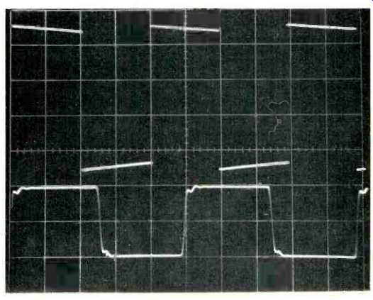
Fig. 6--Top curve, 200-watt, 50-Hz square wave with 8-ohm load (scale: 20V/cm,
5 mS/cm); lower trace, 10-V p-p, 10 kHz square wave into 0.22-uf load (scale:
5 V/cm, 20 µS/cm).
Figure 6 shows a 80-V p-p, 200-watt, 50-Hz square wave into 8 ohms and a 10 V p-p, 10-kHz square wave into 0.22 if.
The 50-Hz waveform exhibits relatively low tilt which is desirable. A reader recently suggested that amplifiers be tested with capacitive loads in the range of 0.05 to 0.2 pF to see if any real amplifier instability occurs. Accordingly, the second trace of Fig. 6 shows the 500D's behavior with 0.22 pF. As capacitance is raised from zero, the circuit starts to ring at about 0.05 pF and rings more and more with decreasing resonant frequency as capacitance increases to the low micro farad range. With this amplifier, no sign of amplifier instability per se was observed. The ringing shown is caused by the RLC network formed by the series buffing inductor typically paralleled by a resistor in the 1-15 ohm range and the capacitance load itself.
Figure 7 is for a 10-kHz, 10-V p-p square wave into a 2-pV load and an 8-ohm resistive load. Ringing with 2 pF is typical of other solid-state amps. The rise time of the resistive load waveform is slower than most other solid-state amps, reflecting the designer's philosophy on required or desirable bandwidth. Of greater interest in this regard, however, is the fact that the rise time as a function of signal level is more constant than any amp so far tested, being about 4-5 µS. Furthermore, at 80-V p-p, the shape is still exponential instead of straight sided which suggests that the amplifier isn't allowed to slew rate limit by the relatively slow overall rise time. (See top trace of Fig. 10.) Fig. 8 shows behavior at 20 kHz into a 1-µF reactive load. The top trace is for square wave drive. Attempts at higher levels simply blew the primary circuit breaker. The level that was achieved (40-V p-p) is suggestive that the amplifier is behaving equally for plus and minus transitions and would probably look good at higher outputs if the breaker would permit. The sine wave level is 40 V rms or 200 volt-amps. THD under these conditions was 0.4%.

Table I--Output noise as a function of bandwidth, in uV.
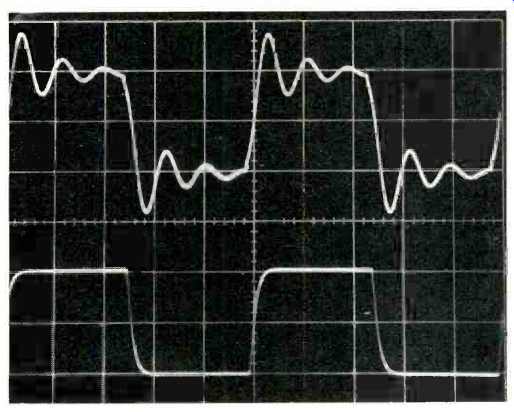
Fig. 7--10-V p-p, 10-kHz square wave into, top, 2-uF load and, bottom, 8-ohm
load. (Scale for both: 5 V/cm, 20 uS/cm.
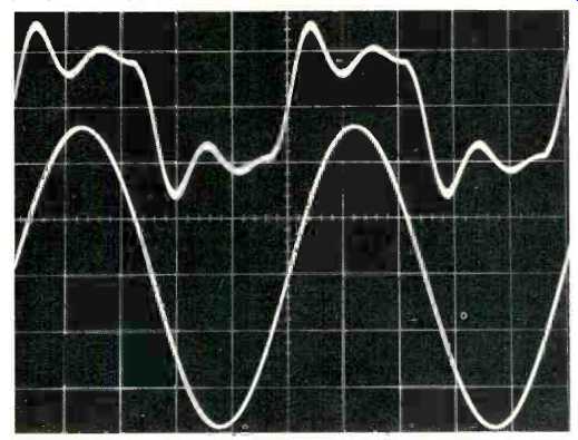
Fig. 8-Behavior at 20 kHz into 1-µF load. Top, square wave; bottom, sine wave.
(Scale for both: 20 V/cm, 10 uS/cm.)
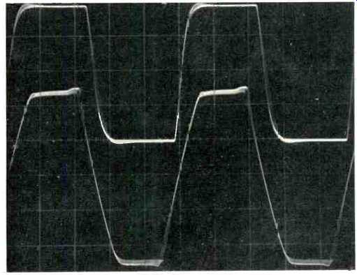
Fig. 9-Top curve, 20-kHz square wave into 8-ohm load; lower curve, 20-kHz
sine wave into 8-ohm load with 2-dB overdrive. (Scale for both: 20 V/cm, 10
uS/cm.)
The top trace of Fig. 9 is an 80-V p-p, 20 kHz square wave into 8 ohms. Note the rise and fall portions are exponential in shape, and both transitions behave about the same. The blurring at the corners is a 120-Hz power-supply-ripple modulation effect that decreases as power is reduced. The lower trace is for a 2-dB overdrive beyond the onset of visual clipping with a 20-kHz sine wave. Not evident in this trace is the sudden reduction of peak amplitude when clipping occurs, which must be accompanied by increased common mode conduction in the output stage, thus dragging down the power supply. "Sticking" per se is relatively absent.
Damping factor was measured as a function of frequency and varied from 225 at low frequencies to 200 at 1 kHz, decreasing to about 25 at 20 kHz. Output noise as a function of measurement bandwidth is shown in Table I below. The higher noise level in the 20 Hz to 20 kHz band was caused by line harmonics, and the 122 µV figure is 110 dB below 200 watts into eight ohms--quite good. Power at 1 kHz at onset of visual clipping into four-, eight-, and sixteen-ohm loads was 380, 231, and 129 watts, respectively.
In summary, the 500D is a strong, well-built amplifier that should be quite rugged in use, especially with lower impedance and capacitive loads. It would be a very excellent choice as a woofer amplifier in a multi-way system. As a wide range amplifier, the 500D will drive difficult loads with stability and safety.
-Bascom H. King
(Audio magazine, Dec. 1975)
Also see:
BGW 500R Stereo Amplifier (Oct. 1973)
BGW Systems Model 203 Stereo Preamplifier-Control Center (Equip. Profile Nov. 1977)
= = = =