
Four independent comparator circuits on one chip can be used in a variety of analog and digital applications.
BY CLEMENT S. PEPPER
THE KEY WORD to describe the 339 quad comparator is versatility. This device can interface a slow-moving analog signal to almost any logic family, will drive a LED, detect highand/or low-voltage limits and can be used as a monostable oscillator.
What makes the 339 so versatile? Consider its power requirements as an example. The chip will work from a single dc source between 2 and 32 volts, or a split power supply from ±1 to ±18 volts. Current drain is a meager 0.8 mA, independent of supply voltage.
The common-mode range includes ground, even when operated from a single supply. With a typical input bias current of 25-nanoamperes, a 3-nanoampere offset and a 3-mV input offset voltage, the input can "look" at almost any source impedance without loading.
The 339 output stage is an npn transistor having an uncommitted collector so that an external pullup resistor can be used with a supply voltage different than that used by the remainder of the device. You can even hard-wire the outputs in an OR configuration. The transistor output stage will sink up to 20 mA, but you may have to live with a high saturation voltage (with 4 mA it is 250 mV). The output is compatible with TTL (fan-out of 2), DTL, ECL, MOS and CMOS. The 339 chip contains four identical comparators, and is available from many parts suppliers at prices as low as $1 each.
Device Operation. The pinout for the 339 is shown in Fig. 1A. The numbers across each row indicate the noninverting and inverting inputs with the associated outputs for each of the four comparators in the chip.
A basic comparator is shown in Fig. 1B. Here, the input signal VIN is compared with a fixed reference VREF. Whenever the input signal exceeds the reference level by just a couple of millivolts, the output (VO) goes high. This action is illustrated by the associated waveforms.
Unfortunately, such a basic circuit can oscillate during the transition period, and although this might present a problem with slow analog signals, it would cause no trouble for the fast transition times associated with digital signals. This can be averted by using a small amount of positive feedback as shown in Fig. 1 C. The feedback not only speeds up the transition, but adds a little hysteresis.
Feedback resistor RF is typically a high value, 10 megohms for example.
While hysteresis can eliminate the transient oscillation, it can also be put to work in a useful manner such as "cleaning up" input waveforms, acting like a Schmitt trigger. However, most Schmitt triggers lack adjustability, and further along in this article, we will illustrate a 339 Schmitt trigger that does not have this problem.
Analog-to-Digital Interface. The input for a frequency counter is a good example of an analog-to-digital interface (not to be confused with an A/D converter as used in computers). The input of a frequency counter must be capable of accepting a wide variety of signals, slow or fast, and provide a signal compatible with the digital counter circuits that follow. Also, since the input levels can span a broad range of levels, sensitivity adjustments are required.
Then there must be a "threshold" established either to reject noise, or possibly to match a digital source. Such a circuit is shown in Fig. 2A. Sine-wave performance (10 kHz) is shown in Fig. 2B with a 3-volt rms input and Fig. 2C with 1-volt rms input. This circuit has been used with excellent results to 1 MHz.
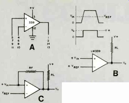
Fig. 1. Pinout of the LM339 (A). Comparator with basic waveforms (B). Comparator
with feedback resistor for faster switching action (C).
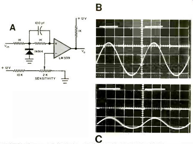
Fig. 2. Counter input circuit (A). Output with 10-kHz, 3-jolt input (B)
and 10-kHz, 1-volt (C). Outputs are upper traces, with 5 V/dir. Sine wares
are at 2 1/(lin.
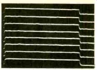
Fig. 3. Outputs of two separate 339 packages (four at top, four at bottom)
show excellent matching.
CMOS to TTL Translation. The circuit shown in Fig. 2A is also useful for translating various logic families. For this application, two series-connected 1 N914 diodes may be substituted for the 2000-ohm potentiometer. This establishes a 1.4-volt reference compatible with both TTL and CMOS operating from a 5-volt supply. The 1000-ohm pull-up resistor connected at the output has to be connected to the TTL 5-volt supply.
During the design of an 8-input oscilloscope circuit, the author connected eight such circuits, with all eight inputs connected to a source having a pulse 8-microseconds wide. The upper four traces of Fig. 3 came from one 339 package, while the lower four traces came from another 339 package. Actual time variations are about 200 nanoseconds. This illustrates the quality of diffusion techniques these days.
High and Low Limit Detection.
Two comparators working together sense the low and high limits in the simplified capacitance measuring scheme shown in Fig. 4A. The unknown capacitor (C) is charged from a constant-current source (I1). This results in a linear charging ramp whose slope is proportional to the capacitance (Fig. 4B). The limit voltages are 0.10 and 1.10 volts, so that the measurement becomes that of the time required to charge the capacitor to this higher voltage.
In the complete circuit (Fig. 4C), the addition of an exclusive-OR gate yields a pulse whose width is scaled to the value of the capacitor. Scope traces of a typical measurement are shown in Fig. 4D. The capacitance can be determined from the width of the pulse.
Earlier in this article, hysteresis was mentioned as one way to get high and low limit detection, such as used in a Schmitt trigger. The circuit shown in Fig. 5A uses a single comparator which does not have the precision of the dual comparator approach but is useful with looser tolerance circuits.
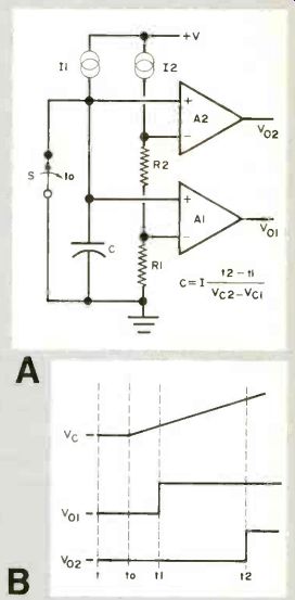
Fig. 4. Basic capacitance measuring circuit (A) and timing diagrams (B).
Complete circuit (nand output for 4.7µF (D).
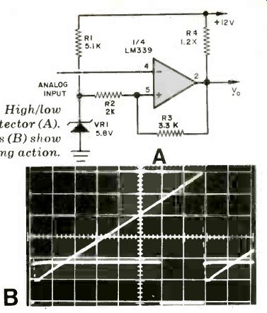
Fig. 5. High/low limit detector (A). Waveforms (B) show switching action.
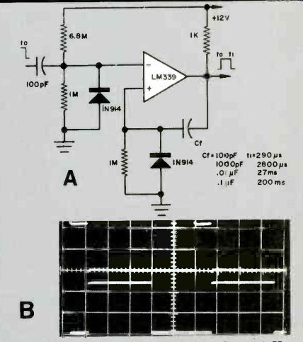
Fig. 6. Monostable circuit (A). In (B) 1710-Hz input is at top, output
below (5 V/div).
Although the circuit appears tricky, it is easy to understand. First, you have to know the desired upper and lower switching voltages. Then, select a zener diode that falls midway between these voltages. Part of the problem comes when trying to get a zener diode of the correct value since zeners come in specific voltages. Therefore, pick the closest value. Select R1 for 5 to 10 mA of zener current.
When the 339 output is low, some of the current through R1 flows through R2 and R3 into the output. We can safely assume that none flows into the noninverting (+) input. Pin 5 of the 339 will now be lower than the zener.
With the 339 output high, current flows through R4, R3 and R2 into the zener diode.
Although we will not go into a detailed circuit analysis, the "trick" here is to select the resistor values. In the circuit shown in Fig. 5A, the switching points are 7.7 and 4.0 volts. Build the circuit and vary the resistor values to get a feel for circuit operation. A typical waveform is shown in Fig. 5B. Monostable. The circuit for a 339 monostable is shown in Fig. 6A, with an output waveform shown in Fig. 6B. The inverting (-) input of the comparator is biased about 1.25 volts positive by the 6.8-megohm and 1-megohm voltage divider.
Triggering occurs on a negative-going input which forces the inverting input below ground. The 1N914 diode limits this to one diode drop. The resulting positive-going output is fed back to the noninverting (+) input, and the timing is determined by the discharge time of the feedback capacitor C_F and the 1megohm resistor. This time is proportional to the capacitance value for the ranges shown in Fig. 6A. Although this circuit may require some "tweaking" to achieve specific monostable action, it is useful to know about if you have an unused comparator in your design and require a monostable.
Source: Computers and Electronics--Experimenter's Handbook (1984)
Also see:
Build ‘LIDITH' -- A 3½-Digit Digital Thermometer