BY ARTHUR F. BLOCK
For best performance from operational amplifiers, special power-supply needs should be satisfied.
OPERATIONAL-amplifier circuits almost always call for power sources that furnish clean, stable dc. Batteries are sources of good dc, but their expense relegates them principally to portable applications where commercial ac power is not readily available.
The more economical solution to the problem of powering op amps is to use a power supply to convert commercial ac into smooth dc. In this article, we will examine several basic power-supply circuits that are well suited for use with operational amplifiers.
Symmetry is one of the principal characteristics required of most op-amp power supplies. Integrated operational amplifiers usually have two power-supply terminals-V + and V. If the voltages applied to these terminals are not symmetrical with respect to the input signal's ground potential (be it earth ground or an "artificial" ground), the output signal will ride on a do level proportional to the power-supply asymmetry. This is usually undesirable-if a dc voltage is to be amplified, there will be error; if an ac voltage is to be amplified, capacitive coupling might be needed to prevent the upsetting of a subsequent stage's bias levels. Also, the possibility exists that the output signal will be asymmetrically clipped.
There are two basic types of power supplies that can be used with operational amplifiers-bipolar and single-ended. In a bipolar supply, positive and negative output voltages (usually equal in absolute value) are generated. The required symmetry arises from the fact that both the positive and negative supply rails are removed from ground by equal but opposite voltages. A single-ended supply generates only one voltage referenced to ground-either positive or negative. The ground of the power supply functions as one of the supply rails, and an "artificial ground" or "signal ground" is synthesized with a resistive voltage divider for reference purposes.
This provides the required symmetry to the circuit.
Each type of supply has advantages and disadvantages. A bipolar supply furnishes a signal ground that is at true ground potential. This simplifies circuit design and eliminates at many points the need for capacitive coupling. However, a bipolar supply is more complex than a single-ended one and is more expensive to construct. A single-ended supply is simpler but usually makes the circuit to be powered slightly more complex. Let's examine some basic supplies of each type and see how they can be used to power op-amp circuits.
Basic Power Supplies. Appearing in Fig. 1 are simple single-ended (A) and bipolar (B) power supplies. In the single-ended supply, bridge rectifier D1 through D4 delivers pulsating dc to filter capacitor C1, which provides a smoothed dc output. Resistor 121 is a bleeder component. A voltage divider comprising R2 and R3 synthesizes an artificial signal ground at half of the positive dc output voltage (assuming R2 = R3) or approximately +17 volts. The op amp's positive power-supply terminal is connected to V + and its negative supply terminal is connected to V-, which is actually true ground. An amplifier powered by this supply can process an ac signal symmetrically if the signal input is at ARTIFIC1AL GROUND and the constraints of the power supply are not exceeded. The use of a blocking or coupling capacitor at the output of the amplifier permits the recovery of a pure ac signal with no dc component.
A basic bipolar power supply appears in Fig. 1B. The major differences between it and the single-ended supply just described lie in the transformer used, the need for a second filter capacitor, and the lack of a ground-synthesizing voltage divider. A transformer with a center-tapped secondary is needed. The bridge rectifier comprising D1 through D4 simultaneously charges filter capacitor C1 positively and C2 negatively. The GROUND at the output of the supply is connected to the transformer's center tap, and the positive and negative output voltages are symmetrical with respect to it. Note that the differential voltage between the positive and negative supply rails in each supply is the same even though the actual voltages on each of the rails with respect to true ground are not the same.
As a rule, operational amplifiers consume small amounts of current. This points to a disadvantage of the bipolar supply shown in Fig. 1B. Because only a small amount of output current is required, compact transformers rated at 300 mA or less are particularly attractive. Unfortunately, small transformers with center-tapped secondaries are not as widely available as ones lacking a center tap. The bipolar supply shown schematically in Fig. 2 offers a solution to this problem.
A glance at this supply reveals that it delivers positive and negative output voltages by means of a transformer lacking a center-tapped secondary. Also, note that the voltage rating of the secondary is half of that of the transformer shown in Fig. 1B. This supply can be thought of in one of two ways-either as two half-wave supplies, one positive and one negative with a common ground, or as a full-wave voltage doubler. In any event, it provides positive and negative voltages approximately equal to those produced by the supply shown in Fig. 1B. Also, the GROUND at the output of the supply is true ground, not an artificial one.
In practice, the true grounds of Figs. 1 and 2 are often connected to earth ground for shielding purposes. A fundamental difference between the bipolar supplies of Figs. 1B and 2 is that larger filter capacitors are required in the circuit shown in Fig. 2 for the same amount of ripple rejection. This is because the ripple frequency is lower (60 Hz as opposed to 120 Hz). Therefore, twice the capacitance is required if the capacitive reactance of the ripple shunt path to ground is to be kept at the same value as before.
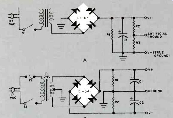
Fig. 1. Single-ended dc power supply for op-amp (A). Bipolar dc power
supply that employs a center-tapped transformer (B).
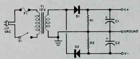
Fig. 2. A bipolar dc supply whose transformer does not have a center
tap.
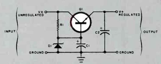
Fig. 3. This electronic filter provides a regulated positive dc output.
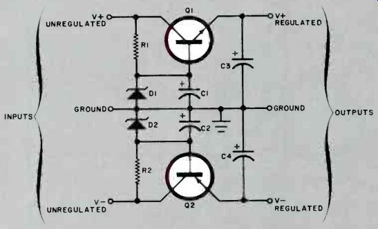
Fig. 4. An electronic filter for use with bipolar dc supplies.
Electronic Filtering. If the current drain from any of the power supplies that have been described is very low, and if the values of the filter capacitors are sufficiently large, only a small amount of ripple will be present in the dc output.
However, in some applications even a low-level ripple component can be troublesome. An excellent safeguard against ripple is the use of electronic filtering such as that provided by a zener diode.
If a zener diode or similar component or electronic filtering network is connected to the output of a simple power supply, ripple can be almost entirely suppressed. The diode will provide not only the equivalent of several thousand or tens of thousand microfarads of filter capacitance in a very small space, but also a high degree of voltage regulation, which is very beneficial.
A basic electronic filter for positive-voltage applications is shown schematically in Fig. 3. When a positive unregulated voltage is initially applied to the input of the filter, capacitor C1 begins to charge up to the input voltage. Zener diode D1 clamps the voltage across the capacitor when the zener knee of its characteristic curve is surpassed. The voltage applied to the base of transistor QI is thus kept at a fixed level. This transistor effectively performs two functions. It multiplies the capacitance of C1 by its dc beta and behaves as an emitter follower, presenting a voltage at its emitter equal to the zener voltage less the forward voltage drop across the base-emitter junction. Capacitor C2 improves the performance of the electronic filter by helping to absorb transients.
The time constant R1 C1 results in a slow turn-on characteristic that eliminates potentially troublesome switching transients (clicks) from the supply rails.
The filter shown in Fig. 3 is designed for use with positive-output (negative-ground), single-ended power supplies. It can be adapted for negative-output applications by inverting the polarities of C1, C2, and DI and employing a pnp instead of an npn pass transistor. The unregulated negative dc voltage would then be applied to the node R 1-collector of Q1 and the regulated negative voltage would appear at the emitter of Q1. This technique is employed in the bipolar electronic filter shown schematically in Fig. 4. The top portion of this circuit is essentially the same as that shown in Fig. 3, and the bottom is a mirror image of the top-that is, a negative-output electronic filter.
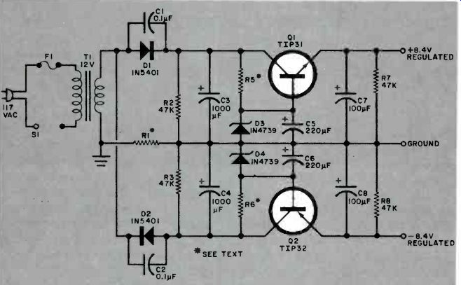
Fig. 5. Complete regulated bipolar supply for op-amp circuits. Transistors
Q1 and Q2 might require heat sinking.
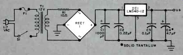
Fig. 6. Regulated single-ended dc supply for powering operational amplifiers.
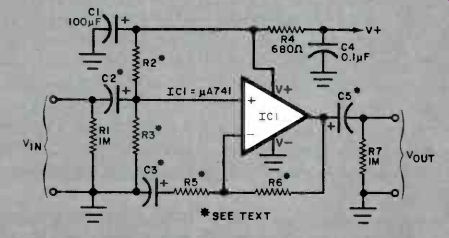
Fig. 7. Typical noninverting op-amp stage designed for use with a single-ended
supply.
Practical Supplies. A complete bipolar regulated power supply for op-amp audio applications appears schematically in Fig. 5. It is basically an amalgam of Figs. 2 and 4 with a few additional elements included. Hum and ripple components in its bipolar outputs are so low in level that they can be ignored in most applications, even where op amps are operating at high gain. The one precaution that is necessary is careful placement of transformer T1. This component should be located as far from high-gain stages as is practicable, and it should be physically oriented to keep induced hum signals as small as possible.
Rectifiers D1 and D2 have forward current ratings of three amperes rms.
This high current rating, together with the current-limiting action of R1, prevents damage to the diodes by excessive charging current to the capacitors when ac power is first applied to the supply.
Actually, the inherent resistance of the 300-mA transformer secondary is great enough to prevent the initial charging current from damaging three-ampere diodes. However, if one-ampere diodes or a transformer with a larger secondary-current rating (and thus less winding resistance) are used, or both, it would be wise to include resistor R1 in the circuit.
The value of this resistor can be determined by measuring the resistance of the secondary and then solving Ohm's law for the resistance necessary to limit the current through the diodes to the rms rating. The peak voltage delivered by the secondary (1.414 times the rms voltage) should be used in this calculation, and the electrolytic capacitors should be considered dead shorts. Thus, only the inherent secondary resistance and any supplemental resistance provided by R1 will be available for current limiting. If the resistance value obtained by this calculation is larger than the resistance of the secondary winding, R1 should be included. Its value is simply the remainder obtained by subtracting the secondary resistance from the total resistance required. This results in a greater degree of protection for the diodes than is really necessary, but ensures trouble-free diode performance.
Note that 0.1-µF disc ceramic capacitors are shown in parallel with each rectifying diode. The function of these components is to suppress the spikes that are generated each time the diode junction breaks into and out of conduction. Fourier analysis of the waveform generated by the diode reveals the presence of significant high-order harmonic components. These harmonics can be troublesome to high-gain op-amp audio stages as well as a source of radio-frequency interference to AM or FM tuners.
Resistors R5 and R6 provide current limiting for zener diodes D3 and D4.
Values of these components are best determined empirically after performing an initial calculation. First, the rated zener voltage should be subtracted from the voltage appearing across C3 or C4.
The remainder is the voltage drop across the current-limiting resistor. Then Ohm's law should be solved for that value of resistance that results in a current flow of two milliamperes through the resistance. Using this as a starting value, connect a suitable component to the rest of the circuit and temporarily connect a load resistor between the regulated output and ground. The load resistance should be such that the supply will be required to source two or three times the amount of current drawn by the op-amp circuit to be powered under worst-case (maximum current) conditions.
Apply power to the circuit and measure the voltage across the load resistor.
Next, disconnect the load from the output of the supply and measure the open-circuit output voltage. If the difference between the loaded and unloaded output voltage is greater than a few percent at most, decrease the value of the current-limiting resistor to the next smaller commercial value and repeat the procedure.
(Alternatively, employ a trimmer potentiometer in place of fixed resistors.) When the supply voltage has sufficient regulation, permanently install a fixed resistor of the next smallest commercial value with respect to the resistance value that has been empirically determined. This will provide an extra margin of voltage regulation.
The use of this empirical method, though somewhat crude, is justified by the fact that many experimenters purchase surplus zener diodes and transistors whose parameters might be unknown or considerably different from their rated values. Parameters such as a transistor's dc beta and the sharpness of a diode's zener knee will have a significant influence on the appropriate values of the current-limiting resistors. If this method does not produce the desired result, that is, if adequate voltage regulation cannot be obtained, either the zener diode or transistor (or both) should be replaced with another component of the same type. Deficiencies in either device can cause this problem.
Some readers might question the choice of the bipolar output voltage, ± 8.4 volts, as opposed to the more common ± 12 or ± 15 volts. The author was more interested in extended, reliable op-amp performance than in large output-voltage swings. A lower supply voltage places less strain on' an op amp and can also help prevent it from becoming noisy. The lower supply voltage does not affect stage gain. However, if a higher differential supply voltage is desired, simply use higher-voltage zener diodes for D3 and D4 and follow the same resistance-selection procedure that has already been outlined.
Keep in mind that the output voltage will be approximately 0.7 volt less than the zener voltage of the diode and that decreasing the differential input-to-output voltage (VcE of the pass transistor)
can degrade voltage regulation when large amounts of current are drawn from the supply. A ± 8.4-volt prototype supply can simultaneously power four op-amp audio stages with fine regulation and lack of hum.
A complete single-ended supply for op-amp applications is shown in Fig. 6.
It generates a regulated +12-volt output referenced to ground and employs a 100-PIV modular bridge rectifier and an integrated 12-volt regulator. Resistor RI limits the surge current through the bridge during power-up. Capacitors C2 and C3 are disc ceramic components that should be placed close to the regulator IC package. Solid tantalum capacitor C4 improves the transient response of the regulator IC. Alert readers might have noted that no spike-suppressing capacitors are shown connected across the bridge's diodes. The capacitors might not be necessary, but any reader who plans to duplicate this circuit should leave space for them if actual performance indicates a need for them. Four capacitors would then be installed-one across each diode forming the bridge.
The + 12-volt output is usually sufficient for most op-amp applications. It permits the output of an operational amplifier to swing almost 12 volts peak-to-peak without clipping. If a greater output swing is desired, a higher-voltage regulator IC and either a diode-capacitor voltage multiplier or a transformer with a smaller step-down ratio can be used.
Figure 7 is the schematic diagram of an op-amp audio amplifier that the author has powered with the single-ended supply just described. Resistors R2 and R3 form a voltage divider across the supply rails. The values of these components are identical (typically 100,000 ohms) so that the noninverting input of the op amp, the one to which input signals are applied via coupling capacitor C2, is at exactly half the supply voltage.
This artificial signal "ground" potential permits the op-amp output to swing symmetrically in response to ac excitation. Components CI and R4 decouple the supply line that feeds the biasing resistors to ensure good performance.
The bias level applied to the noninverting input of the op amp causes the output of the amplifier to remain at this same level during quiescence due to the effectively infinite dc feedback provided by R6. No dc amplification can occur, however, because C3 prevents any dc voltage division by R5 and R7. Resistors R1 and R7 provide dc return paths at the input and output of the stage.
The amplifier's voltage gain equals the quantity (1 +R6/R5) because the stage is noninverting. Selection of these resistor values is made to obtain the required voltage gain. The capacitance of C3 should be large enough that the component's capacitive reactance should be low at the lowest frequency to be amplified. One hundred microfarads or more should be sufficient for most audio applications, especially if the gain-determining resistances are on the order of kilohms or more.
Electrolytic capacitors C2 and C5 couple ac signals into and out of the amplifier, respectively. Their values have an influence on the frequency response of the amplifier. As a rule, the capacitance of C5 must be higher than that of C2 for a given low cutoff frequency because the output impedance of the amplifier is much lower than the input impedance. Practical audio circuits of similar design commonly employ tens of microfarads or more capacitance for input coupling and hundreds or thousands of microfarads for output coupling. The optimum values for a given application depend on the lowest frequency to be amplified, the load impedance, etc.
Some audio circuits employing electrolytic capacitors and op amps powered by bipolar supplies have appeared previously in the literature. These circuits have one principal disadvantage-there is no dc polarizing voltage impressed across the coupling capacitors. During one half of the ac signal cycle, the capacitors are reverse-polarized and a reverse current flow exists. At best, this can result in varying circuit impedances and shortened capacitor useful lifetimes.
At worst, it can cause catastrophic capacitor failure and the application of dc levels from a previous stage to a subsequent one. In the op-amp circuit we have just described, all electrolytic capacitors are properly dc-polarized.
In Conclusion. Operational amplifiers are among the most useful devices available to the electronics experimenter. For best performance, their relatively modest power requirements should be satisfied through the use of stable sources of clean dc. To that end, a number of power-supply design ideas and practical circuits have been presented in this article. The experimenter can use them for guidance in the construction of power supplies that will enable him to derive the best possible results from his op-amp projects.
Source: Computers and Electronics--Experimenter's Handbook (1984)
Also see: High-Speed Electronic Fuse
Low-Cost Power Supplies Recycled AC Adapters