Regardless of whether transistors or vacuum tubes are used in a color receiver, the functions of the several circuit systems remain unchanged.
That is, a solid-state set still has a tuner, IF strip, horizontal and vertical deflection systems, chroma system, etc. Thus, the radical changes brought about by the adaptation of transistors to color-receiver circuitry occur in the circuits themselves, not in the overall design concept. There is one exception to this statement; the use of solid-state devices makes modular construction much more feasible than it was in vacuum-tube designs. A vacuum-tube color receiver of modular construction has been marketed (Setchell-Carlson), and at least one manufacturer is contemplating a solid-state color receiver which does not have modular construction. The relative merits of the two types of construction are not an appropriate subject of discussion here.
Review of Transistors
In presenting the following information, we assume that the technician has some prior knowledge of transistor circuitry. For this reason, we will not dwell on the theory of their operation. The physical laws which govern the operation of solid-state devices have been published many times and the interested reader may pursue the subject by studying any of a host of books. For our present purposes, we will consider most of the transistors used in a color receiver as "black boxes" which amplify.
It is worth noting that some of the characteristics of transistors dictate significant changes from conventional tube circuitry. In their most usual configuration, transistors exhibit very low input impedance.
For this reason, resistors in the circuit arc usually relatively small and capacitors have relatively large values.
Fig. 1 will help to illustrate this important point. Assuming that each circuit must operate at 1 kHz. we will calculate the value of C1 which will allow reasonably good energy transfer from the first stage (represented by a generator) to the second stage. As a general rule of thumb, the impedance of the coupling capacitor should not exceed 1/10 of the impedance of the input circuit of the following circuit. In the vacuum-tube circuit (Fig. 1 A) the maximum impedance of C1 may be n5 greater than 50K ohms and the capacitance may be calculated by:
To maintain the same impedance ratio between coupling capacitor and input, the value of C1I in the transistor circuit (Fig. IB) may not exceed 47 ohms.
Because large coupling capacitors are necessary, it is sometimes more practical to eliminate them entirely and couple successive stages directly. This is also done in vacuum tube circuitry where response to very low frequencies is desirable, but each direct-coupled stage requires, roughly, at least 100 additional volts from the power supply, a serious limitation. Transistors operate from more moderate voltages than tubes, and several stages may be direct coupled even though the power supply produces only 100 volts or less. By using alternate NPN and PNP transistors in a direct-coupled cascade, an almost unlimited number of stages may be direct coupled without increasing the power-supply voltage.
While the use of direct-coupled transistor stages is desirable from the point of view of economy and design simplicity, it may introduce a troubleshooting problem. A direct coupled amplifier will pass DC as well as any other frequency, and so any change in emitter-to-base DC potential of the first stage is amplified in each following stage. Thus, if a shift in bias of 0.1 volt should occur at the front end of a string having a gain of 100, a change in output of 10 volts would result.
In practical applications, a DC swing of 10 volts is nearly impossible because some transistor in the string probably would either saturate or cut off at a smaller shift in bias. The result is the same-the problem area is in front of the circuit where the symptoms are most likely to be detected.
DC feedback loops and current limiters are often used in transistor circuits to prevent the runaway condition just described. The circuit shown in Fig. 2 has such a feedback path. (The circuit is not in the Motorola receiver.) Assume that the positive base voltage of Q9 de B+ creases for some reason. The conduction of Q9 will decrease, causing the base voltage of Q10 to rise. The increased conduction of the collector of Q10 causes an additional drop across R51, and the base of Q 11 becomes less positive. This causes increased collector current in Q11 and the collector swings positive because of the increased drop across T1.
Without a feedback loop, a small decrease in bias at the base of Q9 might well cause such a large increase in collector current through Q11 that the transistor would be damaged. The feedback loop consists of R55, C19, and R54, connected between the collector of Q11 and the base of Q9. By virtue of this loop, as the collector voltage of Q11 tends to rise, a portion of this positive-going voltage is coupled back to the base of Q9 to increase its conduction. Thus, the action of the feedback loop is always to oppose any change in the DC operating potentials of the transistors. Note that C19 acts as a low-pass filter in the feedback loop.
Because of it, only DC, or low frequency AC, is fed back to Q9.
In our discussion about the DC feedback loop, we assumed that the potential at the base of Q9 changed for some unspecified reason. While idle conjecture about the cause of this shift is pointless, it is true that changes within Q9 itself, or variations among transistors in a production run, are a major source of the variations. Thus, we may conclude that DC stabilization is required for two reasons: the DC instability of direct-coupled amplifiers, and the inherent DC instability of transistors themselves.
In general, it is also true that the gain stability of transistors is poorer than it is for vacuum tubes. For this reason, an AC feedback loop also may be incorporated in an amplifier string. Referring again to Fig. 2, the AC feedback network consists of R53 and C49. A portion of the amplifier output is fed back to the input in phase opposition.
Thus, if the gain of the overall circuit increases, so does the amplitude of the inverted signal fed to the input, and the gain is maintained constant. Note that this feedback circuit incorporates a high-pass filter so that it is insensitive to DC. Another characteristic of transistors which is sometimes confusing to the technician is the manner in which they fail. Although a triode with a grid-to-plate short is quite rare, a base-to-collector short in a transistor is a distinct possibility.
Furthermore, while a grid-plate short probably would be destructive to associated components, a base collector short may cause no external damage. A transistor with a base-collector short may pass the signal (without amplifying it, of course) but there will be no inversion of the waveform.
Typically, vacuum tubes fail because of gradually decreasing cathode emission and lowered trans conductance. This is unlike transistors which usually maintain a nearly constant gain throughout their lives; failures are due to shorts or excessive leakage.
Motorola 23TS-915 and 919 Chassis Chroma Circuitry
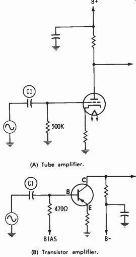
Fig. 1. Comparison of transistor and vacuum-tube amplifiers.
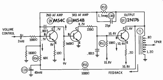
Fig. 2. Feedback loops in a transistor amplifier.
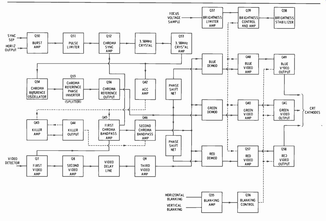
Fig. 3. Detailed block diagram of the Motorola solid-state chromes circuits.
Fig. 3 is a block diagram of the chroma circuits used in the Motorola 23TS-915 and 919 chassis. Although most of us are accustomed to only about half this number of blocks, the functions performed by this chroma circuit and one using vacuum tubes are essentially the same. With the exception of the demodulators and color amplifiers, which are rather novel, the entire chroma circuit is quite similar to a vacuum-tube design.
Reference Circuits
Following the same sequence that was used in Section 4 of this guide, we shall examine the reference-signal circuits first. Video from the first video amplifier is fed to the first chroma-bandpass amplifier, which has two outputs. One of these outputs, consisting of the chroma side bands and the color burst, is fed to the chroma-sync amplifier. The chroma-sync amplifier is the equivalent of the burst amplifier of conventional designs and is a coincidence gate. Also fed to the chroma-sync amplifier is an enabling pulse from the burst amplifier and pulse limiter. This pulse gates the sync amplifier on at the time when the color burst is present at its input, allowing it to pass. During the remainder of the scanning interval, the sync amplifier is gated off, removing the chroma sidebands from its output.
The color burst from the sync amplifier is developed across the 3.58-MHz crystal, causing it to ring from one burst to the next.
The crystal is amplified by Q53 and the output of this stage is a CW signal which is re-phased at the start of each horizontal scan.
The chroma-reference oscillator, Q54, is a Colpitts oscillator which free runs during black-and-white reception. However, if a color burst is present, the output from the crystal amplifier phase locks the oscillator, causing its output to be in phase with the color burst.
The chroma-reference phase inverter is actually a splitter which develops two out-of-phase signals from the single input. A potentiometer across these outputs, the hue control, selects the specific phase of reference signal required for correct hue of the picture.
Finally, the reference signal is amplified by Q56 and fed to the three demodulators. The phase of the signal from Q56 is correct for the green demodulator, and phase shifting networks develop the correct phase for the blue and red axes.
ACC and Color Killer
A portion of the output from the 3.58-MHz crystal amplifier is rectified and fed to the ACC amplifier.
If the amplitude of the burst increases, the output of the crystal amplifier increases, and this, in turn, causes the bias developed in the ACC amplifier to increase. This decreases the gain of the first chroma bandpass amplifier to maintain a constant-amplitude output with a varying input. (See "Closed Loop ACC" in Section 5 of this guide.) The output of the ACC amplifier also is supplied to the killer amplifier, Q43. In conjunction with Q44, the killer output stage, Q43, operates as an electronic switch. That is, the circuit is either cut off or saturated-there is no "in between." In the absence of a color burst, the killer cuts off the second chroma-bandpass amplifier; when a burst is present, the second chroma-bandpass amplifier is turned on. The color intensity control is located in the network between the killer and the second bandpass amplifier.
Bandpass Amplifiers
The two chroma bandpass amplifiers, Q45 and Q46, are straightforward in design. As stated above, the gain of the first stage is controlled by the ACC amplifier and the second stage is cut off during monochrome reception by the color killer circuit. The color intensity control also is incorporated in the input of the second bandpass amplifier. The two stages are tuned to pass sidebands having frequencies up to 500 kHz above or below the burst frequency.
Chroma Demodulators
The diode chroma demodulators used in this receiver are similar in many respects to the ones used in some General Electric receivers.
The essential difference is that a third input, the luminance (or Y) signal is also fed into the three Motorola demodulators.
Today, the majority of color receivers recombine the luminance signal and the ,three color-difference signals within the CRT. (See Section 4 of this guide.) This practice was adopted because of its relative simplicity and economy, but it makes the ability of the receiver to track the gray scale dependent on the degree of nicety with which the three guns of the CRT can maintain identical trans-conductances. The concept of recombining the luminance and chrominance information outside the CRT allows more accurate adjustment of gray-scale tracking and the possibility of correcting for long-time variations in CRT parameters and also for changes in the external circuits.
Time will tell whether or not this second-generation external matrix will fulfill expectations.
The three demodulators of Fig. 3 are identified simply by the color (not color-difference) signals which they produce. This is entirely proper, since color-difference signals never appear in this chassis; chrominance and luminance information are recombined (matrixed) in the demodulators. One of the demodulators will be examined in detail later in this article.
Color Amplifiers
Each of the color demodulators is followed by a pair of amplifiers which raise the signal level to an amplitude sufficient to drive the CRT cathodes. These amplifiers are direct coupled, allowing the brightness control to be connected to the emitters of the first stages of each amplifier string. Making the emitters of Q40, 048, and Q57 more positive causes the collectors to swing in the same direction. This swing is inverted in the output stages, driving the CRT cathodes negative and increasing the brightness.
The emitters of 041, Q49, and 058 (NPN types) return to ground through the blanking-control transistors Q36. When Q36 is cut off during horizontal and vertical retrace, the video-output transistors also are cut off, driving the CRT cathodes positive into cutoff.
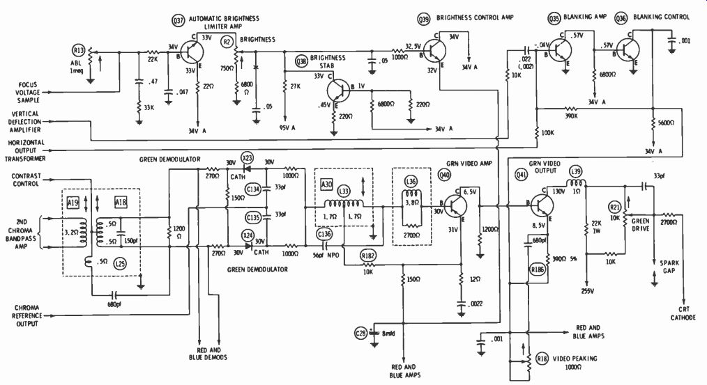
Fig. 4. Motorola demodulator and color amplifiers.
Brightness Circuit
The brightness circuit, Q37, Q38, and Q39, includes the manual brightness control and also an automatic brightness limiter (ABL). The purpose of the ABL circuit is to maintain constant CRT beam currents (for a given brightness control setting) even though shifts in video-amplifier gain, line voltage, horizontal-output voltage, etc. might tend to change the brightness. Also, the ABL control allows the technician to preset the maximum brightness for optimum operation.
A sample of the focus voltage is used as a control voltage for the ABL. Any shift in brightness will shift the level of the control voltage.
For example, if the CRT brightness decreases for some reason, the focus voltage will increase. A positive going control voltage increases conduction of the video amplifiers, video outputs, and the CRT guns to increase brightness.
Blanking Circuit
Positive pulses derived from the vertical sweep amplifier and from the horizontal-output transformer are coupled to the blanking-control stage, Q36. by the blanking amplifier. These pulses cut off the video output transistors during retrace.
To reduce the load on the horizontal-output circuitry. the horizontal retrace time of this chassis is longer than usual and the CRT is over-scanned slightly. The width of the horizontal-blanking pulse is increased accordingly, and it is normal for a portion of the first color bar from a keyed-rainbow generator (yellow-orange) to be partially blanked and off the left side of the raster.
Chroma-Circuit Analysis
The three demodulators are practically identical, with the exception of the phase of the reference input and the value of the input attenuation. Since it serves no useful purpose to treat them separately, only the green demodulator is shown in Fig. 4.
During reception of a black-and white signal, there are two inputs to the demodulator. A free-running, 3.58-MHz signal is fed to the junction of C134 and C135. Positive video from the contrast control, situated in the output circuit of the third video amplifier, is fed to the center of the secondary of L25.
There is no input from the chroma bandpass amplifier, since it is cut off by the color killer.
The reference signal produces no output at the base of 040 because of the traps, L33 and C 136, between the demodulator and the video amplifier. These same traps remove the 3.58-MHz ripple during color reception.
Positive video (a positive signal makes a black raster) passes through X24 and is developed across R 182. The video passes through the trap and is duly amplified by the two video amplifiers and fed to the CRT cathode. Of course, the same things take place in each of the other demodulators and their amplifiers. Thus, the luminance signal is amplified and fed to the three CRT cathodes to produce a monochrome picture.
The operation of diode chroma demodulators is discussed in detail in Part 5 of this guide.
To summarize, if the reference and chroma signals are in phase, a maximum output of one polarity is realized; if they are out of phase, a maximum output of the opposite polarity results; if they are 90° out of phase, the output is zero. In the demodulator of Fig. 4, in-phase signals produce a negative voltage at the base of Q40 and increase the CRT conduction, voltage at the base of Q40 and increase the CRT conduction.
So far, we have considered the chrominance and luminance signals separately, but, since both of these signals are developed across the same resistor, R 182, they are effectively added at this point. This sum (or difference) of the two signal voltages passes through the traps, which remove the 3.58-MHz ripple, to the base of Q40 and, ultimately, to the CRT.
Blanking Control
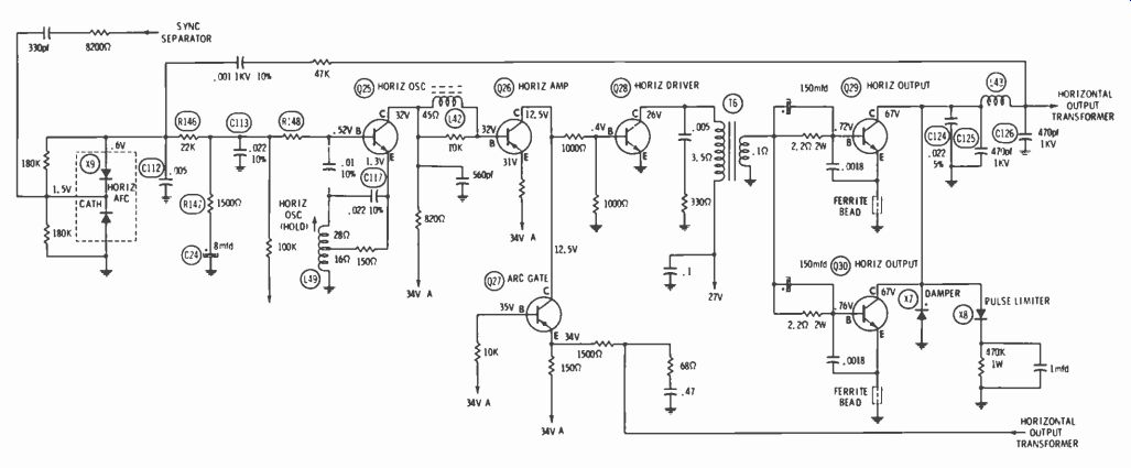
Fig. 5 Solid-state horizontal-oscillator and output circuit.
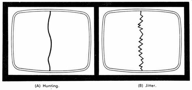
Fig. 6. Appearance of horizontal hunting and jitter . (A) Hunting. (B) Jitter.
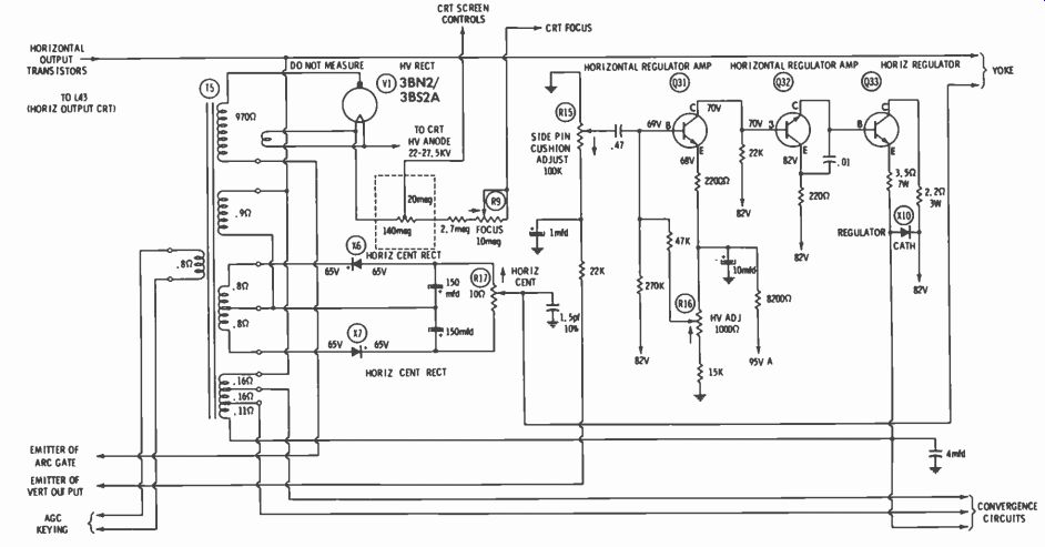
Fig. 7. Horizontal regulator circuit.
The blanking and brightness control circuits also are shown in Fig. 4, not because the functions they perform are novel, but because the use of transistors results in unusual circuit configurations The emitter currents of the three color-video output transistors must al flow through the blanking-control transistor, Q36. During scanning time, Q36 is forward biased and the complete circuit path of the collector current of Q41 is from ground, through Q36, R186 and Q41 to the CRT cathode and the 255-volt supply.
During retrace, Q35 is driven to saturation by the positive pulse on its base. This removes the forward bias from the base of Q36, cutting it off. This effectively opens the low-resistance path from ground to the emitters of the video-output transistors, cutting them off.
Automatic Brightness Limiter
The level of the sample of focus voltage taken from the low end of the CRT screen-control potentiometer indicates the total load on the high-voltage and focus-voltage supplies, and hence, the amount of CRT conduction, or brightness. The adjustment of R13, the ABL control, determines the size of the sample (control voltage) taken and acts somewhat as a coarse control of the brightness.
Q37 is connected as an emitter follower, roughly equivalent to a cathode-follower tube configuration, and the emitter voltage is dependent on the amplitude of the control voltage. Because of Q37, the voltage at the top of the brightness control cannot become more positive than the 34-volt supply at the collector of Q37. This limits maximum brightness of the CRT. The voltage on the base of 039 is determined by the setting of the control voltage. Q39 also is connected as an emitter follower, and the voltage on its base controls the bias on the video amplifiers, Q40, Q48, and Q57. Notice that the base voltage of Q39 is stabilized by Q38, which acts as a regulator for the circuit.
Analysis of Horizontal-Deflection Circuits
Space is not available for an analysis of all circuits in the Motorola solid-state chassis, so this discussion is necessarily limited to those of greatest significance. In addition to the chroma circuits already covered, the design of the horizontal deflection system is sufficiently different from designs using tubes to justify an analysis.
Horizontal Oscillator and AFC
The horizontal oscillator and the AFC circuit (Fig. 5) which controls its frequency are very similar to designs using tubes. The AFC circuit compares the phases of the horizontal sync pulse and the output of the horizontal-output transistors, Q29 and 030, to develop a control voltage. This control voltage is integrated by R146, R147, C24, C112, and C113, and it is used at the base of Q25 to control the oscillator frequency.
The function of the integrating circuit between the AFC detector and the oscillator is not particularly mystifying, but it appears, from the number of letters we receive, that malfunctions in this circuit cause a great number of problems to our readers. The following comments apply to nearly all sets, vacuum tube or solid-state.
Failures in the integrator fall into four general categories:
(1) Loss of control voltage caused by R 148 going open, for example. In this case, there is no horizontal sync.
(2) Radical change in the DC level of the control voltage which causes a radical change in horizontal frequency, or may cut off the oscillator.
(3) Too much integration of the control voltage.
(4) Not enough integration of the control voltage.
The first two categories named above are generally not too difficult to diagnose, but the last two seem to cause many difficulties. If the control voltage is integrated too much, the response time of the system becomes too great. Therefore, the raster appears to slowly move back and forth across the CRT. The complete raster will not necessarily float the same amount, and so a vertical line on the CRT may curve back and forth from top to bottom (see Fig. 6A) . This is called horizontal hunting.
Too little integration causes the oscillator frequency to be overcorrected. With insufficient integration, the control voltage at the oscillator (or AFC tube) shifts slightly during each scan. This causes the scanning time of each horizontal line to be slightly different and a vertical line on the CRT appears ragged or broken as shown in Fig. 6B. This is called horizontal jitter.
Jitter is usually caused by a decrease in value of C24 (or its counterpart in another set), hunting is usually caused by an increase in resistance of R146 or R147, or their counterparts.
Referring again to Fig. 5, the horizontal oscillator is a Hartley oscillator; L49 and C 1 17 determine the frequency. When the top of the tank is negative, Q25 is cut off. As the top of the tank swings positive, the transistor begins conduction at some point on the sine wave. This point is determined by a combination of fixed bias and the control voltage from the AFC. The collector current of Q25 is a series of pulses and the waveform at the base of Q26 is approximately a square wave.
Amplifier, Driver and Output
The train of pulses is fed to the driver through the horizontal amplifier, and the output of the driver is coupled through T6. The phasing of T6 is such that the output transistors are turned on when the driver is cut off. Deflection of the trace from center to the right edge of the CRT occurs while Q29 and Q30 are conducting. At the instant that Q29 and Q30 are cut off, the sweep retraces, the damper begins conduction, and the left side of the raster is scanned.
The network consisting of C124, C125, C126, and L43 is a low-pass filter which prevents any high frequency transients which may be generated in the amplifier, driver, or output stages from being coupled to the horizontal-output transformer. The pulse-limiter diode, X8, limits the amplitude of the collector pulses of Q29 and Q30 to protect them.
In case of a high-voltage short, a positive pulse is developed at the emitter of Q27, causing it to conduct. This clamps the base of 028 to the base of Q27, causing it to conduct and cutting off the horizontal-output transistors until the arc clears.
Horizontal Regulator and Pincushion Circuit
The circuit which includes Q31, Q32, and Q33 (Fig. 7) performs the two functions of injecting a portion of the vertical deflection signal into the horizontal sweep system for pincushion correction, and it also regulates the high voltage. Both of these functions are accomplished by controlling the supply voltage for the horizontal-output transistors.
A parabolic voltage derived from the emitter of the vertical-output transistor is amplified by 031 and Q32 and added to the supply for the horizontal output transistors.
The supply voltage is increased when the vertical sweep is at the center of the tube, causing the horizontal scan to expand at this time to correct for pincushion effect.
R15 picks off the amount of vertical sweep voltage which is required for optimum correction.
At the same time, the relative values of the 82-volt supply and the 95-volt supply are compared in the emitter-base circuit of Q31. As CRT beam current increases, the load on the horizontal-deflection circuit increases and the output of the 82-volt power supply drops.
This decreases the forward bias of Q31, causing the collector voltage to increase. This increase in collector voltage increases the conduction of Q32 and 033, which tends to raise the supply voltage to the horizontal-output transistors, thereby regulating the high voltage.
Admiral's K10 Hybrid Color Chassis
To reduce the possibility of damage occurring in one section while working on another, Admiral has designed two etched-circuit boards: One contains the solid-state circuitry; the other, the vacuum tubes.
These etched boards are separated into zones by heavy white lines.
Each zone is identified by a large white letter designating the section.
A-Video IF B-Sound. AGC, and video amplifiers C-Chroma amplifiers D-Chroma oscillator and color killer, color burst amplifier, and color demodulators E-Vertical F-Horizontal G-Convergence H-Miscellaneous chassis components U-UHF tuner V-VHF tuner This coding system also makes it easier to find the components on the schematic. Resistor RC64 on the wiring diagram will be found in zone "C", with the number "64" written beside it on the board.
Circuit Description
Admiral chassis K10 is comprised of twenty-six transistors, twenty-four diodes, seven vacuum tubes and a CRT. The transistors are used for all signal-processing functions, while the vacuum tubes are used in circuits that have heavier power requirements.
Power Supply The power transformer is used only for the transistor circuits, although it does have a 6.3-volt AC tap to supply filament voltage to the CRT. A line choke is used to prevent any unwanted RF signals from entering the various circuits through the source voltage.
Video IF Strip (Fig. 8)
The outputs of the first and second video IF transistors are applied across tuned coils. These coils are shunted by a pair of capacitors to form a capacitance voltage divider.
The input signal for the next stage is obtained from the junction of these capacitors. This configuration results in the proper impedance match for efficient signal transfer.
The sound "take-off" is from the collector of the third video IF. Sound Circuits.
The sound section consists of the sound takeoff, sound IF, oscillator limiter, ratio detector, audio driver and audio output stages.
Oscillator Limiter
The oscillator limiter stage is self oscillating, with the frequency determined by the incoming signal from the sound IF stage. This incoming sound signal serves as a "sync" signal for the oscillator limiter. Because of the dependency of the output of the oscillator on the incoming signal, the output of the oscillator does not change in amplitude and is, therefore, a very effective limiter stage. The output of the oscillator limiter is then applied to the ratio detector.
AF Sound Circuitry
The AF sound circuitry has two direct-coupled transistors driving an output transformer. A voltage dependent resistor (VDR) is connected across the primary of the audio output transformer to prevent damage to the receiver if it is operated with the speaker disconnected.
The output transistor is mounted on the end of the chassis, utilizing the chassis as a heat sink. A mica wafer isolates the collector (transistor case) from the chassis, resulting in a potential of 105 volts DC on the transistor case.
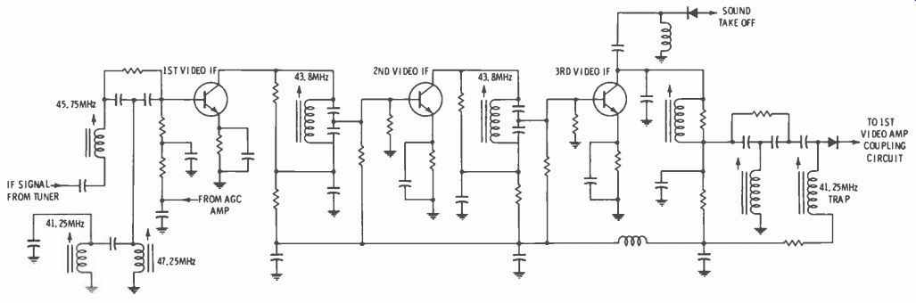
Fig. 8 Three-stage transistorized video IF employed in Admiral's K10 hybrid
chassis.
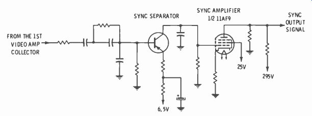
Fig. 9 Transistor and vacuum tube are mated in sync separator/amplifier section
of K10.
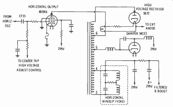
Fig. 10 Fuse in cathode circuit of horizontal output stage provides overload
protection for horizontal output and flyback.
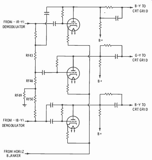
Fig. 11 Triple-triode 8AC10 performs color-difference amplification function
in Admiral's hybrid chassis.
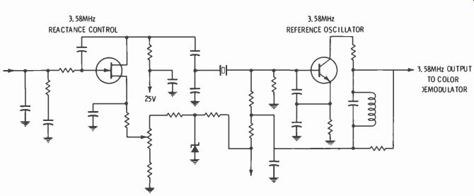
Fig. 12 Field-effect and conventional NPN transistors serve in the reactance
control and chroma reference oscillator section of the K10's chroma circuitry.
Sync and Sweep
A transistor is used as a sync separator with its output driving a vacuum-tube (11 AF9) sync amplifier (Fig. 9). The sync output voltages are taken from the plate and applied to the vertical and horizontal circuits.
The horizontal phase detector and horizontal oscillator are similar to those used in previous Admiral models.
The horizontal output stage (Fig. 10) operates as a controlled switch.
It conducts during half of the scan line, and is cut off the other half.
When drive pulses are applied to the grid coupling capacitor (CF33), grid rectification produces an extremely high negative grid voltage.
When the output tube conducts, heavy current flows through the flyback windings. At the end of the line scan, the output tube ceases conduction, and the flyback field collapses, providing the flyback pulse. This pulse is stepped up by the high turns ratio of the high-voltage transformer windings. It is then rectified by the high-voltage regulator which provides the high CRT anode potential. As the collapsing flyback field shifts into its negative half cycle, the damper tube becomes forward biased, causing a strong damper current to flow. The yoke current will then increase and conduct in the same direction as the output tube. The damper causes the beam to sweep the remaining half line.
Simultaneously, the boost capacitor is charging up to boost level.
The dampered flyback field will produce an output that is added to the B+ potential. This boost voltage is filtered and used to supply the CRT screen voltage, vertical oscillator plate and vertical output bias requirements.
The horizontal output circuit is protected by a fuse in the cathode of the horizontal output tube. This circuit protection, which hasn't been used in a few years, saves the fly hack. The HV regulation is provided by a "pulse feedback" circuit.
Chroma Oscillator
The reactance control stage provides (when necessary) a correction voltage to the 3.58-MHz subcarrier oscillator (Fig. 12). An N-channel junction field-effect transistor (FET) performs this function. Because FET's are susceptible to damage from static discharges and arcs from the CRT, care must be exercised when working in this area. One method of testing is to check for the presence of voltage on the gate of the FET when the 3.58-MHz oscillator is slightly off-frequency.
Check operating potentials on the gate, drain and source, and compare the readings to the voltage values shown on the schematic.
As with most control circuits, the reactance control does not operate when the subcarrier oscillator remains on frequency. Varying the feedback correction voltage from the color phase detector or changing the setting of the reactance control potentiometer will initiate conduction in the FET. This changes the tuning, or phase, of the 3.58-MHz subcarrier oscillator.
Color Demodulation
Color detection is accomplished using-(R-Y) and-(B-Y) signals.
The output of the demodulators is then inverted and amplified by the color difference amplifiers, and becomes R-Y and B-Y. The demodulators are essentially electronic switches with the 3.58 MHz subcarrier signal directing their operation. The amount of conduction is determined by the amplitude of the chroma signal delivered to them by the bandpass amplifier.
The color demodulators used in the K 10 chassis are PNP transistors.
The chroma signal from the bandpass amplifier is applied to the emitters of the demodulators through a resistive voltage divider network.
The switching signal (3.58 MHz) is fed to the base of each demodulator.
Under these conditions, the negative-going peaks of the 3.58-MHz signal will cause conduction, and an amplified color difference signal will be present on the collectors of the demodulators.
To control the time of demodulator conduction, the 3.58-MHz signal is coupled directly to the-(R Y) demodulator and through a phase shift network (90°) to the -(B-Y) demodulator. The 3.58 MHz signal present on the collectors of the demodulators is trapped out by a capacitance/inductance network.
Fig. 13 Cutoff of transistorized horizontal blanker during horizontal retrace
drives cathodes of color difference amplifiers more negative; difference amplifiers
become saturated and their plate voltage decreases, biasing off CRT grids.
Fig. 14 Transistor buffer amplifier supplies 3.58-MHz reference signal to
color-killer and phase detector diodes.
Fig. 15 Color-killer and associated detector circuitry.
Color Difference Amplifier (Fig. 11)
The color difference amplifiers arc housed in a three-section triode tube, type 8ACIO. The outputs of the color demodulators are fed through the difference amplifiers, and the signals are amplified, inverted and applied to the CRT red, blue and green grids. The-(R-Y) and-(B-Y) signals come directly from the demodulators, and the-(G-Y) signal is formed by a matrix circuit comprised of resistors RF43, RF46, RF49 and RF50. Horizontal Blanker (Fig. 13)
To accomplish horizontal blanking, each color difference amplifier is biased off during horizontal retrace time. A negative blanking pulse is applied to each color-difference amplifier cathode, causing heavy conduction through the triodes, producing a high-amplitude pulse on the CRT grids. The color difference amplifier is driven into saturation, the plate voltage is decreased sharply, and the CRT is driven into cutoff. This action results in some signal detection, which provides a measure of DC restoration to the CRT. The horizontal blanker stage cuts off the CRT during horizontal retrace time by driving the color difference amplifier into saturation.
The PNP transistor acts as a switch at the horizontal rate.
During the horizontal scan time, the horizontal blanker conducts strongly, due to the biasing action of the base resistor, RC48. During the retrace interval, a positive pulse from the flyback transformer drives the base-emitter junction into a reverse-bias condition, and the transistor becomes an open switch. The collector voltage decreases to zero.
When the cathode bias voltage of the color difference amplifier is removed (horizontal blanker collector at zero volts), the color difference amplifiers are driven into saturation.
The plate voltage decreases sharply, cutting off the CRT grids.
3.58-MHz Reference Feedback System (Fig. 14)
A buffer amplifier (3.58-MHz reference feedback amplifier) supplies a 3.58-MHz reference signal for the color-killer detector diodes and the phase detector diodes. The color demodulator diodes control the phase of the redeveloped chroma subcarrier.
The 3.58-MHz signal is coupled to the base of the buffer amplifier.
The tint control, RH34, and capacitors CD81 and CD82, connected across inductance LD80, are connected in the collector circuitry and alter the phase of the output signal, controlling the color demodulation when the tint control is varied. Inductor LD27, capacitors CD26, CD28 and resistor RD29 restore the phase of the reference signal applied to the killer detector.
Color Killer System (Fig. 15)
The color-killer amplifier cuts off the first bandpass amplifier when no color information is present in the received signal. When no color information is present, the color-killer amplifier conducts heavily, driving the first bandpass amplifier to cutoff. This prevents color noise from contaminating the b-w picture.
When color information is present in the signal, the detected burst signal is applied to the base of the killer amplifier. When the killer amplifier is cut off, no killer bias is applied to the first bandpass amplifier and it is free to amplify the chroma signal.
When color information is not present, a positive voltage, derived from the color-killer control (connected to the 25-volt line), supplies forward bias to the killer amplifier through the color-killer detector diodes.
When color information is present, the color signal is detected and a negative voltage is developed to cancel the forward-bias voltage RCA's CTC40 Color Chassis RF Amplifier (Fig. 16 & 17)
A dual-gate MOS field-effect transistor is used in this stage. Operation of this device (shown in Fig. 1) is as follows: A dual-gate FET functions in much the same manner as two vacuum tubes connected in a cascade configuration. Internal feedback capacitance, which tends to cause amplifier instability (oscillations), is defeated by the relatively low input impedance of the driven portion of the FET. Because of this characteristic of the FET, neutralization is not necessary at VHF frequencies. RF gain control is accomplished by reverse biasing of gate G2. This reverse gain-control voltage reduces the amplifier gain by reducing the drain current of both sections of the FET. Since this control voltage (reverse bias) is derived in combination with the chassis circuitry, it actually forms the RF AGC. Circuit Operation (Fig. 17)
Signal from a 300-ohm antenna input is applied to an impedance matching circuit on the cabinet back to match the 75-ohm input impedance of the receiver. This signal is fed to gate GI of the FET through the high-pass filter network and the RF tuned circuitry. The RF AGC voltage is applied to gate G2 of the FET. This voltage may range from-5.0 volts on a very strong signal to a 6.7 volts on an extremely weak signal. The bias for gate GI is comprised of a portion of the AGC voltage applied through resistor 121 and the voltage developed across the source resistor, R2.
In this circuit the source and gate GI voltages will coincide or vary with applied AGC, minimizing input capacitance variations. Printed inductances are utilized to couple the RF amplifier output signal to the mixer input circuit.
Mixer (Fig. 18)
The mixer stage is also connected in a cascade configuration, using two transistors. Transistor A operates in a common-emitter circuit and its output drives a common-base amplifier. As with the FET RF amplifier, the principal advantage to this type of circuit is its inherent stability.
The base bias network for transistor A is comprised of resistors R1, R2, R3 and R4. This bias voltage is maintained at a value designed to allow the most efficient mixing action. Transistor B base bias is derived from a biasing network composed of resistors R2, R3 and R4.
Fig. 16 Circuit diagram illustrating the basic operation of the dual gate
MOS FET employed in RF amplifier.

Fig. 17 Simplified schematic of RF amplifier employed in CTC40 chassis.

Fig. 18 Mixer stage employing two transistors in cascade arrangement.
The output, or resultant IF signal, is coupled from the mixer by a circuit configuration called "low-side C." The IF output signal is developed across capacitor C1. This capacitor is connected from coil L1 of the tuned output circuit (L1 and C2) to ground. From this circuit configuration comes the term low side C. This coupling arrangement tends to minimize the amount of oscillator energy that might be coupled into the IF circuit. At oscillator frequencies coil L1 acts as an RF choke and greatly reduces the amount of oscillator energy developed across C1.
Oscillator (Fig. 19)
The local oscillator is basically a Colpitts-type arrangement. Energy at the selected frequency of the oscillators is developed across the tank circuit. The inductance of the tank is composed of L1 (channel 13 adjustment) and the oscillator coil, which changes for each channel selected. The capacitance of the tank is supplied primarily by capacitor C1 and the AFT transistor. Oscillation is sustained by a capacitive voltage divider made up of the transistor internal capacitance existing between the emitter and collector (CCE) and the emitter and base (CEB). Capacitor C2 couples the oscillator transistor output to the tank circuit.
Automatic fine tuning is provided by transistor Q2. The internal capacitance of this transistor varies in proportion to the AFT control voltage applied to its collector and base terminals. This transistor then controls a portion of the oscillator tuning capacitance and, thus, the frequency output of the oscillator.
The KRK-132 UHF Tuner The UHF tuner used in the CTC 40 chassis is a KRK-132 and has been used previously with several other RCA chassis. It contains no physical or electrical changes from those originally used.
Video IF Circuits The CTC40 IF section contains three common-emitter amplifier stages (see Fig. 20) capable of supplying a maximum of 80 dB gain to frequencies within the limits of the IF bandpass. This IF bandpass is established through the proper tuning of eight tuned circuits located within the IF system. Alignment of these circuits is very similar to the alignment process of similar RCA circuits employed in tube-type receiver chassis.
Gain in the first and second IF stages is under AGC control and it is possible to reduce the overall gain of the IF section up to 70 dB under very strong signal conditions.
Link Coupling (Fig. 21)
The IF signal contained in the output of the mixer stage is link coupled to the first IF amplifier.
The link coupling circuit used in the CTC40 chassis is very similar to other recent RCA color chassis. The circuit is basically a double-tuned, or overcoupled, network consisting of the mixer collector coil, coupling capacitor, the first IF base transformer and two trap circuits with their associated capacitors. The link coupling components are essential in obtaining a good IF response curve.
It is necessary that they be aligned and adjusted exactly. The correct curve is shown in Fig. 22. The manufacturer's specifications or other accurate service data should be consulted for the correct procedures to obtain this response.
First and Second Video IF Amplifiers
The first and second video IF amplifiers are identical. Both are common-emitter types employing identical input and output circuits.
The input coupling circuit to the base of each amplifier consists of a series resistance/capacitance combination. This coupling circuit provides DC blocking and highly efficient impedance transfer. Their output signals are developed identically across single-tuned circuits.
Bias for the first and second IF amplifiers is obtained as follows: The second IF amplifier receives base bias voltage from the output of the AGC inverter stage. This identical voltage (less the small drop across the second IF amplifier base emitter junction) is applied to the first IF amplifier. In this manner both the first and second IF stages receive almost identical AGC control voltages. The emitters of both the first and second IF amplifiers are returned to ground through a 450-ohm, 7-watt wirewound resistor. The positive temperature coefficient properties of this resistor function to vary the bias on both transistors and compensate for long-term temperature-related gain changes. The emitters of both stages are bypassed by a capacitor.
Third Video IF Amplifier (Fig. 23)
The third video IF amplifier is a common-emitter configuration whose output is applied to the video detector, AFT, and sound circuits.
The base bias is derived from a voltage network comprised of resistors RI and R2. The source voltage for this network is taken from the collector resistor (R3) of the third IF amplifier transistor. DC negative feedback is obtained from this arrangement, which improves bias stability. Emitter bias is obtained, or determined, by resistor R4. This resistance is AC bypassed by capacitor Cl. Due to the high gain (40 dB) of the third IF stage, neutralization is a necessity, and it is provided by feedback capacitor C2.
The overall frequency response, which is determined by the efficiency of the link circuit, the interstage tuned circuits and the third IF amplifier output, is illustrated in Fig. 23.
Again, please refer to the manufacturer's data sheet or PHOTO FACT for information relating to alignment procedures.
Video Detector The video detector circuit (Fig. 24) does not differ greatly from the circuits previously used in tube-type chassis. Harmonics of both the detected carriers and difference frequency signals are bypassed by Cl.
The 4.5-MHz difference frequency developed by mixing the picture and sound carriers is removed by a 4.5 MHz bridged-T trap composed of coil L1, capacitor C2 and resistor R1. L2 and L3 decrease harmonics developed by detector functions.
The DC component of the detected video signal is retained by using the average DC level produced by the detector as the major portion of the first video amplifier base bias. The detected video signal is applied across the detector load impedance comprised of resistor R2 and peaking coil L4. This voltage is series added to the comparatively small 'second detector pre-bias voltage derived from the 15-volt supply by a resistive divider network made up of resistors R3, R4 and R5. This voltage sets the initial bias level for the first video amplifier, and also provides a constant emitter bias for the gated AGC amplifier.
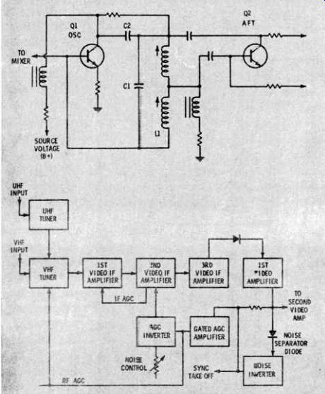
Fig. 19 Local oscillator and AFT circuitry employed in KRK-142 VHF tuner.

Fig. 20 Block diagram of tuner and video IF circuits employed in CTC40 chassis.
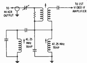
Fig. 21 Double-tuned link coupling is used between mixer output and video
IF input.
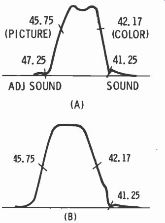
Fig. 22 Correct response curves of (A) link coupling circuit and (B) overall
video IF circuit.
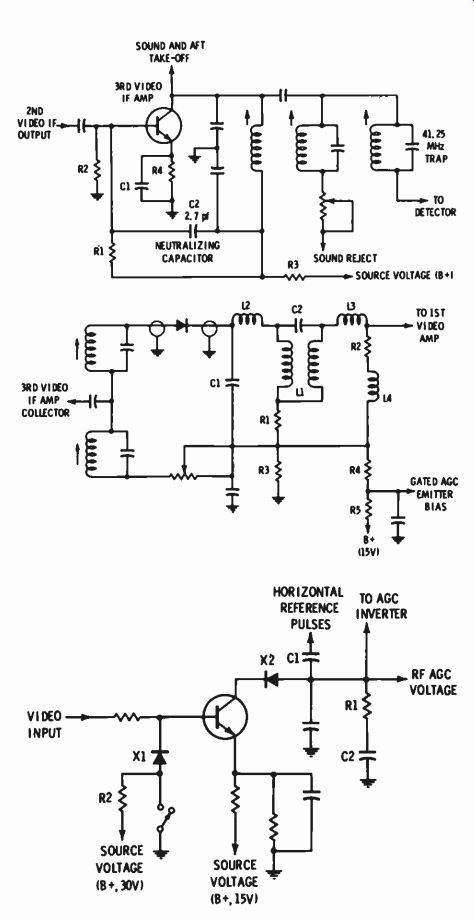
Fig. 23 Third video IF amplifier employed in CTC40 chassis.

Fig. 24 Video detector circuit of CTC40 Is similar to the design employed
in previous tube-type chassis.

Fig. 25 Gated AGC system Is keyed on by positive going sync pulses applied
to base and collector.
AGC
The purpose of any type of AGC is to maintain a constant video detector output level over a wide range of input RF signal levels. The changes or variations in video signal amplitudes are translated into DC voltages which are used to control the gain of the RF amplifier and the first and second IF amplifiers.
in the CTC-40 chassis.
Video information from the first video amplifier is fed to the gated AGC amplifier to produce an output DC voltage that is proportional to the sync tip amplitude. This AGC output is filtered and applied simultaneously to the RF AGC clamp circuitry and the IF AGC inverter.
The RF AGC clamp circuit sets the requirements of the AGC voltage variations that can be applied to the RF amplifier. The RF amplifier operates under reverse AGC control. A more negative voltage (reverse bias) results in gain reduction, and a more positive voltage (less reverse bias) results in increased gain.
An AGC inverter stage is required for the first and second video IF stages to satisfy their requirements for forward AGC control voltage.
The AGC inverter base bias is made variable by the noise control, to establish the proper proportions of AGC voltage applied to the RF and IF stages.
Gated AGC Circuit Operation (Fig. 25)
A video signal which contains positive-going sync pulses is fed to the gated AGC amplifier base. (This signal level is proportional to the picture carrier strength.) The gated AGC amplifier is designed to conduct only during sync pulse time by the positive-going keying pulses coupled to the collector through capacitor Cl. These pulses occur at the horizontal frequency rate and key the transistor simultaneously with the horizontal sync pulses contained in the video signal applied to the base. The bias on the transistor is such that the base-emitter junction can become forward biased only during the positive peaks of the sync pulses. This circuit keeps spurious noise to a minimum.
During conduction time, electron current flow is from the emitter to the collector, leaving a negative charge on capacitor Cl. This negative charge becomes the AGC voltage and its value is directly proportional to the amount of amplifier conduction; and the amount of amplifier conduction is directly proportional to the peak positive amplitude of incoming sync pulses. The RC network, composed of R1 and C2, improves the overall stability of the circuit.
Service Switch It is necessary to provide a blank raster to aid in picture tube setup.
A positive voltage is applied to the AGC amplifier by operation of the service switch. When the service switch is actuated, a 30-volt potential (normally dropped across resistor R2) forward biases diode X1 and appears on the base of the AGC amplifier. This potential is sufficient to saturate the AGC amplifier and, consequently, produces a high negative AGC voltage. This voltage, in turn cuts off the RF amplifier, and the first and second video IF amplifiers. All video information is removed from the CRT, and a blank raster results. Diode X2, in the collector circuit of the AGC amplifier, prevents the developed negative AGC voltage from discharging back through the collector-base junction between keying pulses.
AGC Inverter (Fig. 26)
The first and second video IF stages require forward AGC control voltages; therefore, it is necessary to invert the AGC output before application to the IF circuits. This is the function of the AGC inverter stage illustrated schematically in Fig. 11. It is a common-emitter DC amplifier designed for a gain of approximately 0.15. Fractional gain is necessary to reduce the large voltage range of the AGC amplifier to within the bias base control limits of the IF amplifiers.
The AGC inverter base bias voltage can be varied by the noise control.
The noise control is used to set the proper proportions of AGC voltages applied to the RF and IF amplifiers throughout the AGC control range.
The control is used basically to establish the point at which the AGC voltage starts reduction of RF amplifier gain, or, if you prefer, sets the RF AGC delay point. Changing the bias on the AGC inverter stage by changing the noise control setting varies the bias and the gain of the first and second video IF amplifiers. The gain of these two amplifiers sets the video signal level applied to the gated AGC amplifier, whose output determines the RF AGC voltage. The noise control should be adjusted while observing a noise-free signal and rotating the noise control in the opposite direction until the snow is gone.
Noise Inverter (Fig. 27)
The purpose of a noise inverter circuit is to prevent any spurious noise pulses that might be present in the video signal from interfering with the smooth operation of the AGC amplifier or upsetting the sync separator. The noise inverter minimizes the effects of any noise pulses by inverting and, thereby, cancelling the pulses before they are applied to the AGC and sync circuits.
The circuit operation of the noise inverter is as follows: A reverse bias is fed to the cathode of X1 from the constant source potential available at the emitter of the gated AGC amplifier. This potential sets the conduction threshold for the diode.
Diode XI conducts only during the interval of positive-going pulses.
These pulses forward bias the diode and are applied to the base of the noise inverter through diode X1 and capacitor C1. The noise inverter transistor does NOT have a DC forward bias; therefore, conduction will occur only when an incoming positive pulse exceeds the base emitter barrier junction potential of 0.6 volt. The positive-going sync pulses fed through diode X1 and capacitor C1 are only at approximately 0.2 to 0.3 volt amplitude and are insufficient to cause conduction.
Only noise pulses in excess of 0.6 volt will trigger the noise inverter into conduction. When the noise inverter does conduct, the noise pulses that triggered the stage into conduction appear amplified and inverted in the collector circuit and cancel the noise pulses coupled to the collector from the first video IF amplifier. Resistor R1 is connected in series with diode X1 to limit the peak conduction rate. This is required to reduce charging of capacitor C1. If this capacitor is allowed to charge excessively, noise inverter action would be blocked until the capacitor discharged to its initial level.
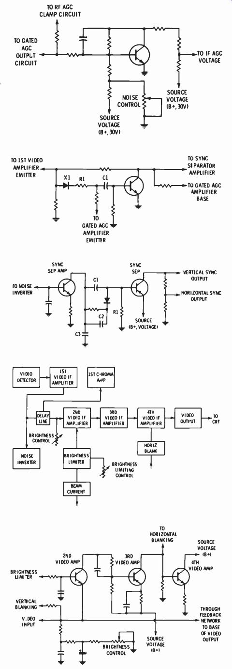
Fig. 26 AGC inverter provides forward AGC control of the 1st and 2nd video
IF stages.
Fig. 27 Noise inverter prevents spurious noise signals from upsetting AGC and sync operation.
Fig. 28 Two-stage sync separator supplies positive going sync pulses to horizontal and vertical sync circuits.
Fig. 29 Block diagram of video amplifier section employed in CTC40 chassis.
Fig. 30 Simplified schematic of the 2nd, 3rd and 4th video amplifier stages.
Sync Separator (Fig. 28)
The sync pulses present at the collector of the noise inverter are applied to the sync separator amplifier base. The output of the sync separator amplifier is of the correct polarity and amplitude to drive the sync separator.
The sync separator is a PNP common-emitter switch which is triggered into conduction by the negative-going sync pulses applied to the base through capacitor C1. Discharge path for coupling capacitor CI is through resistor R1. The output of the sync separator is made up of positive-going sync pulses which are developed across a voltage divider network and applied to both horizontal and vertical deflection systems. The noise immunity features of the sync separator are enhanced during horizontal sync time through the use of 0.01-pf capacitor C1, which provides coupling between the stages. Capacitors C2 and C3 provide filtering for high video and chroma components of the incoming signal.
Video Amplifier Section (Fig. 29)
First Video Amplifier
The output of the video detector is effectively in series with the base bias of the first video amplifier.
Base bias is developed by a voltage divider network. The first video amplifier is connected in an emitter follower configuration. This circuit features a high input impedance to match the inherently high output impedance of the detector circuit. Output of the emitter-follower is developed across a 1000-ohm resistor in the emitter circuit. Additional circuit loading results from coupling to the following stages: The output circuit of the first video amplifier is connected to the first chroma circuit, the second video amplifier, the sync separator amplifier, the noise inverter and the AGC gate.
Delay Line
The signal output of the first video amplifier is coupled to the delay line. The delay line must be properly terminated to prevent ringing, faulty color registration, etc.
The CTC40 delay line has a characteristic terminal impedance (input and output) of 680 ohms at video frequencies. A 560-ohm resistor, in combination with the first video amplifier output impedance, provides the delay line with the proper 680-ohm input terminal impedance.
The output terminal of the delay line is applied to the second video amplifier through a 680-ohm resistor. The second video amplifier stage is designed to exhibit an AC input impedance of zero ohms.
Therefore, the output of the delay line is effectively coupled to AC ground through a resistor to properly satisfy termination impedance requirements.
Second, Third and Fourth Video Amplifiers
The simplified circuit configuration illustrated in Fig. 30 points up the relationship of the second, third and fourth video amplifiers. From a functional standpoint their operation is so similar that a brief discussion of the operation of each will suffice.
Second Video Amplifier
The second video amplifier utilizes a common-base configuration and is designed for an input impedance of zero ohms. This is accomplished through the use of a 10mfd bypass capacitor. The stage functions as a power amplifier. Any fluctuations in the DC output of the first video amplifier are amplified throughout the range of video frequencies. This stage provides proper impedance matching between the delay line output and the third video amplifier input. Positive-going pulses at the vertical frequency rate are fed to the emitter to provide vertical retrace blanking.
The operating point of the second video amplifier varies with the setting of the brightness control. Any change in the brightness control results in a change of the operating point by changing the forward bias current. The lower the resistance of the brightness control, the greater the forward bias current. The result is a larger average current flow through the second video amplifier load resistance. This current flow is translated by the remaining video amplifiers as a reduction in CRT cathode bias and, consequently, an increase in brightness.
Third Video Amplifier
The third video amplifier employs a PNP transistor in a common-base configuration. The video signal is fed to the base through a 1000-ohm resistor. This resistance provides proper loading for the second video amplifier and impedance matching between the second and third video amplifiers. It also functions to prevent saturation of the third video amplifier in the event the second video amplifier develops a collector emitter or emitter-ground short circuit. The output signal is developed across an 1800-ohm load resistor and direct coupled to the base of the fourth video amplifier.
Fourth Video Amplifier
The fourth video amplifier is connected as an emitter-follower. The output of the stage is developed across an 1800-ohm resistor and is direct coupled to the base of the video output transistor. Positive bias voltage applied to the collector is decoupled from the chassis 30 volts supply source by a filter network comprised of a 10-ohm resistor and an .01-pf capacitor. This decoupling 'network prevents feedback loops that could cause low frequency smear, etc. Horizontal pulses, which occur simultaneously with the horizontal retrace interval, are fed to the base to accomplish horizontal retrace blanking. This circuit operation is as follows: Horizontal pulses originating at the high voltage transformer are applied through a clamp transistor to an isolation diode. The isolation diode is reverse biased during scan time by a positive DC voltage developed at the collector of the clamp transistor. During this interval the blanking circuit is isolated from the fourth video amplifier to prevent loss of high-frequency components.
The negative-going horizontal pulses, fed to the isolation diode during retrace intervals, overcome the diode reverse bias and permit it to conduct. These negative-going pulses are present at the base of the fourth video amplifier and are of sufficient amplitude to affect cutoff.
These pulses are applied to the CRT through the video output stage. This action causes picture tube cutoff, or a dark screen, during horizontal retrace time.
Brightness Limiter
A brightness limiter circuit is employed in the CTC40 chassis to hold the CRT beam current within proper limits. The drive potential of the horizontal deflection system is such that, with a high, non-limited brightness control adjustment, it is very possible to exceed the current capabilities of the CRT. Brightness limiting action of the CTC40 functions to reduce the forward base bias voltage on the second video amplifier when the preset limit of CRT beam current is attained. The preset limit is 1600 micro-amperes (1.6 ma). Circuit action is as follows: The high-voltage transformer secondary winding is returned to B+ through the brightness limiter control. Therefore, all beam current drawn by the CRT must pass through the brightness limiter control. Connected between the low side of the brightness limiter control and ground is the brightness limiter transistor. The fixed base bias for this stage makes the voltage across it comparatively independent of the current through it, as long as it is conducting. This action is much like that of a zener diode; the zener voltage being determined by the resistive divider network in the limiter base circuit.
The current through the brightness limiter control has two parallel paths: one through the brightness limiter transistor, and the other through the CRT. If the brightness control is adjusted in such a manner that the CRT is cut off, the only path for current flow is through the brightness limiter control and the brightness limiter transistor. When the CRT is cut off, this current will be 1.6 ma, the desired CRT beam current limit. Should the brightness control be adjusted so that the CRT starts drawing current, part of the current will flow through the CRT and the remainder through the limiter circuitry, the total current flow remaining at 1.6 ma.
The constant voltage applied to the emitter of brightness limiter supplies a regulated bias voltage of approximately four volts to the base of the second video amplifier throughout the range of the brightness limiting system.
When the brightness control is set to the point where the CRT draws the total preset current of 1.6 ma, all of the current flowing through the brightness limiter control is beam current. Therefore, there is no current available to sustain conduction of the brightness limiter transistor. This results in a loss of the constant voltage applied to the base of the second video amplifier. If more current is demanded by the CRT, the voltage on the emitter of the brightness limiter transistor decreases, reducing the forward bias voltage on the second video amplifier. This action results in a decrease of average conduction in the second video amplifier, and a decrease in brightness and CRT beam current, holding beam current within the preset 1.6 ma limit.
Video Output (Fig. 31)
The video output circuitry is reminiscent of previously employed tube-type configurations. It consists of a common emitter amplifier whose input is DC coupled to the emitter of the fourth video IF amplifier, and whose output is DC coupled to the CRT. The contrast control is used to vary the value of the series emitter resistance. The contrast control is AC bypassed by a 30-pf capacitor.
This circuit action (varying the AC bypass of the contrast control) effectively controls AC degeneration with the end result of effective gain, or contrast, control.
Further control of the stage is provided by capacitor C1, which functions to reduce high-frequency degeneration and prevent changes in high-frequency response (peaking) at different contrast control settings.
Inductance and capacitance components form a 3.58-MHz trap which functions to reduce the effects of interference resulting from the mixing of chroma signals and high frequency video signals.
Output loading of the video output stage presents a familiar circuit configuration. Identical circuits have been employed in several previous RCA chassis.
Sound Section
An integrated circuit (IC) contains the bulk of the sound section.
This IC performs the functions of sound IF amplifier, detector and audio driver. For circuit analysis purposes, the IC can be considered as made up of three parts, each section representing a specific circuit function. The first section functions to amplify the incoming 4.5-MHz IF signal to a useful level. The output of the first section (sound IF amplifier) is applied to the second, or FM detector, section. The FM detector removes the audio portion of the signal, which is then applied to the audio driver, the third section of the IC. The purpose of the audio driver is to raise the amplitude of the audio signal to the level required to drive the audio output stage.
Detailed Circuit Analysis (See Fig. 32)
The 4.5-MHz FM sound signal is generated in the conventional "mixing" method by diode Xl. This signal is coupled by IF transformer L1 to the sound IF amplifier section of the IC. The output signal from the sound IF amplifier is applied to the phase shift transformer, T2, and, in turn, to the ratio detector diodes. The output of the ratio detector is the audio signal, which is capacitance-coupled to the volume and tone controls. The audio signal is then capacitance coupled from the volume control to the audio driver section of the IC. The audio driver section functions to provide the required current gain to raise the signal to a level sufficient to drive the audio output stage, Q1.
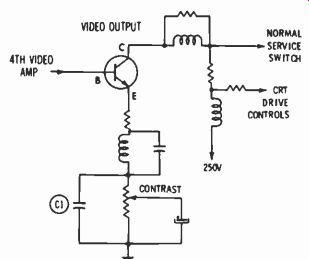
Fig. 31 DC coupling is employed in the input and output of the video output
stage.
The audio output stage is a common-emitter, class A amplifier. The transistor is protected against high amplitude voltage spikes by a 275 volt zener diode connected from collector to ground. DC stability is enhanced by a feedback network (R1, R2) connected from the emitter of the audio output stage to the input of the audio driver section.
Capacitor C1 provides low-frequency compensation for this feedback network. Resistor R3, located between the base and emitter of the audio output stage, functions to provide an additional load for the driver section. This minimizes the effects of output transistor leakage current.
Automatic Fine Tuning (AFT)
The fundamental AFT system is illustrated in Fig. 33. This system is basically the same as that previously used in the RCA CTC30 chassis.
In this system, an integrated circuit (IC) discriminator/amplifier produces a differential DC voltage that is proportional to the applied IF frequency. This signal is then applied to a special "variable capacitance" transistor in the VHF tuner and a varicap diode in the UHF tuner that produce a correction voltage for application to the local oscillator.
Shown in Fig. 34 is a simplified schematic of the CTC40 AFT circuitry. The IC utilizes an internal, regulated power supply and does not require an external reference voltage for defeating the UHF AFT function. Automatic degeneration of the output amplifiers is such that it eliminates all AFT correction signals when the output terminals are shorted for AFT defeat action.
The AFT system is disabled during VHF channel change by the same method used to accomplish AFT defeat during fine tuning--shorting together of the AFT control-voltage outputs. This combination defeat action is initiated by a single switching mechanism built into the plastic housing located on the front of the VHF tuner shaft.
The two 15-mfd electrolytic capacitors, C1 and C2, act to prevent undesired correction voltages generated during channel change time from affecting the local oscillator frequency. These capacitors also function to remove residual video information from the AFT output terminals, allowing only the undistorted DC correction voltage to reach the tuner.
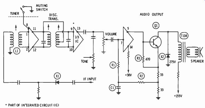
Fig. 32 An IC functions as the sound IF amplifier, detector and audio driver
in the CTC40 chassis.
Fig. 33 Simplified illustrations of the CTC40 AFT system.
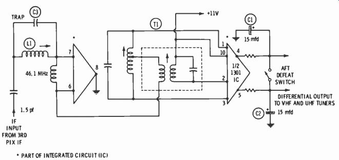
Fig. 34 Simplified schematic of the AFT circuitry.
AFT Operation
The IC AFT circuit is a type TA5360 that functions as follows: A sample of the video IF output is applied to the AFT system through a coupling capacitor located in the collector circuit of the video IF amplifier. This signal is applied to a tuned input circuit comprised of L1 and C1. Coil L1 and capacitor C1 perform a dual role: They act as both an adjacent channel sound trap and as an IF frequency peaking circuit. Correct trap frequency is obtained automatically by peaking the input tuned circuit (L1, C1) at 46.1 MHz.
The output of the input tuned circuit is applied to the buffer amplifier section of the IC, the output of which appears across the primary windings of the discriminator transformer, T1. The discriminator primary is tuned to 46.1 MHz; the secondary winding is peaked at 45.75 MHz.
The discriminator transformer secondary windings feed the IC discriminator diodes. The output voltages of the diodes are applied to an amplifier that delivers a differential voltage output. This differential output contains two voltages, one appearing at each of the IC output terminals. The difference existing between these two voltages (differential) is indicative of the amount and direction the incoming 1F signal deviates from the desired 45.75-MHz frequency. If the incoming IF signal is exactly 45.75 MHz, each output signal voltage will be exactly 6.5 volts, and no differential voltage will exist. When the incoming IF signal deviates from 45.75 MHz, one output voltage will increase, and the other will decrease an equal amount. The voltage at each output terminal will increase or decrease, depending on which direction the incoming signal deviates from 45.75 MHz. The maximum differential voltage produced by this circuit is +9 volts, well within the "pull-in" range of the AFT system.
Vertical Sweep
Basic System
The fundamental vertical sweep system employed in the CTC40 chassis is illustrated in Fig. 35. The integrator sweep circuit consists of a high-gain amplification system operating in conjunction with an integrating capacitor. Operation is as follows:
At the start of vertical trace, the integrating capacitor, C1, is charged from a voltage source. This capacitor charge causes the amplifier to supply yoke current, resulting in a voltage being developed across the feedback resistor, R1, which is coupled directly to the integrating capacitor. This feedback action maintains the amplifier input voltage at a constant level, producing a constant rate of voltage "build-up" across the integrating capacitor. The voltage developed across the feedback resistor is directly proportional to the yoke current; therefore, increase of the yoke current is constant, and a linear scan is produced.
The vertical sweep rate is determined by an electronic switch which discharges the integrating capacitor at a 60-Hz rate. Vertical sync pulses are applied to the switching transistor and determine the exact instant the switch is pulsed "on". This action synchronizes the vertical switching action with the transmitted vertical scanning interval. The "linearity clamping" transistor provides the initial charging current to the integrating capacitor.
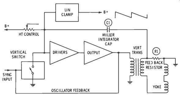
Fig. 35 Illustration of the fundamental sweep system employed in the CTC40.
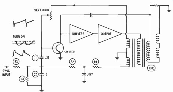
Fig. 36 Partial schematic of the vertical switch and associated circuitry.
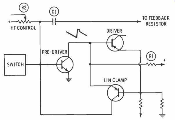
Fig. 37 Schematic showing basic circuitry of linearity clamper stage.
Vertical Switch (Fig. 36)
The function of the vertical switch is to provide a discharge path for the integrating capacitor at the end of each vertical scan interval. This action causes beam retrace and prepares the circuit for the next vertical scan function. Operation of the vertical switch is made self-sustaining by the action of two feedback paths: One path, consisting of resistors R1 and R2 and capacitor C1, is applied to the base and provides the appropriate pulse to initiate "turn on". Vertical sync pulses, from the sync separator, are integrated by resistors R3 and R4 and capacitor C2 and add to the triggering waveshape. An additional feedback voltage is applied to the switch from the vertical output transformer via the vertical hold control. This additional voltage causes the switch base to pass rapidly through the "turn on" voltage potential. As a result, switch "turn on" is extremely stable and comparatively immune from random noise pulses. The vertical hold control has some control of the "turn on" point and, therefore, the frequency at which the circuit operates.
Linearity Clamp (Fig. 37)
Since it is necessary to provide a sufficient amount of initial charging current for the integrating capacitor, a special clamping circuit called the "linearity clamp," is utilized. Operation of this circuit is as follows: The action of the vertical switch discharging capacitor, C1, also cuts off the predriver transistor. This produces a positive voltage on the collector of the predriver. This voltage is of sufficient amplitude to forward bias the linearity clamp transistor. The linearity damper conducts; current flows through the transistor via R1 and the vertical switch. The vertical switch turns off after approximately 700 microseconds, and the linearity clamp then rapidly charges capacitor C1.
As the charge rapidly builds up on capacitor C1, the predriver and driver stages start to conduct, causing the linearity clamp base-emitter junction to become reverse biased due to the voltage drop across the driver base-emitter junction. This circuit action cuts off the linearity clamp and originates vertical scan.
Capacitor C1 continues to charge through the height control, R2, for the duration of scan time.
Vertical predriver and driver (Fig. 38)
The vertical driver section is comparatively more familiar. It consists of two stages: a predriver (NPN transistor operating as a common emitter amplifier) directly coupled to a driver (PNP transistor operating as a common-emitter amplifier). Emitter supply voltage for the driver stage is obtained from a voltage divider network composed of R1 and R2. The driver collector load is comprised of R3 and the base emitter junction resistance of the vertical output stage.
Provisions for picture tube setup are provided by switch S1, which functions to "short" the driver emitter to ground when actuated. The waveshape of the input signal to the predriver is determined by the charging action of the integrator capacitor, C1, which is charged through the height control, R3. The height control supply voltage is made relatively immune to temperature induced variables by the action of thermistor R4. A degree of dynamic regulation for the circuit is provided by a signal from the horizontal deflection system. The insertion of this voltage tends to maintain a constant vertical sweep or height, regardless of horizontal scan and high voltage fluctuations.
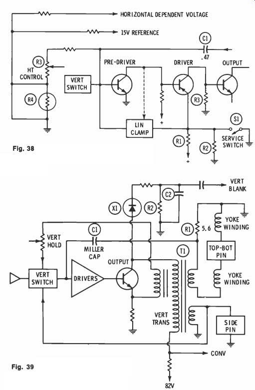
Fig. 38 A two-stage vertical driver section feeds the vertical output stage.
Fig. 39 Common-emitter amplifier is employed in vertical output circuit.
Vertical Output (Fig. 39)
The function of any vertical output circuit is to provide the power necessary to fulfill the vertical deflection requirement of the CRT beam. In the RCA CTC40 chassis the vertical output stage is a common-emitter amplifier with an input from the driver stages. Loading for the vertical output stage is provided by the vertical output transformer, T1, and the vertical convergence circuit.
The vertical output transformer is loaded by the vertical windings of the yoke, two feedback networks, and the pincushion correction circuit. Integrating capacitor C1 is connected to the output circuit by resistor R1, a 5.6-ohm feedback resistor in series with the secondary windings of the vertical output transformer and the vertical yoke windings. There are two feedback networks connected to the vertical switch transistor from the vertical output circuit; both of these networks perform waveshaping functions to provide stable, self-sustaining vertical switching. Diode X 1, in conjunction with capacitor C2 and resistor R2, provides a protective clamping action for the vertical output transistor. Positive-going retrace voltage pulses cause diode X1 to conduct, effectively clamping the vertical output collector to the voltage existing across capacitor C2. A relatively slow discharge path is required for capacitor C2. This is provided by resistor R2. This discharge action sufficiently reduces the voltage across C2 during retrace time to insure the necessary voltage difference across diode X1 when retrace pulses occur. The pulses that appear across capacitor C2 during conduction of X1 are applied to the 2nd video IF stage to provide vertical retrace blanking.
Pincushion Correction (Top and Bottom)
Fig. 40 Top and bottom pincushion correction in the CTC40 chassis is accomplished in a manner similar to methods used in previous RCA color chassis.
A signal voltage derived from the horizontal yoke circuit is coupled to transformer T1. This action energizes a circuit composed of capacitor CI and coil L1, which is tuned to 15,750 Hz and is in series with the vertical yoke windings, L2 and L3.
The resultant sine wave is added to the vertical yoke current waveshape in the proper phase and amplitude to effectively correct top and bottom pincushion distortion. A limited amount of control over the correcting sine wave phase and amplitude is provided by variable inductor, L1, and the damping resistance of R1.
Side Pincushion Correction (Fig. 41)
Side pincushion correction is accomplished by amplitude modulation (at a vertical rate) of the horizontal deflection current. This produces an increase in horizontal scanning width at the center of the raster with respect to the width at the top and bottom. This operation is made possible through the utilization of the saturable reactor circuit illustrated in Fig. 41.
A parabolic waveshape occurring at the vertical frequency is initiated by the action of the control winding of transformer T1, capacitor C1 and resistors R1 and R2. This waveform, coupled to the horizontal yoke circuit by transformer T1, modulates the amplitude of the horizontal yoke scanning current, producing the proper change in raster width.
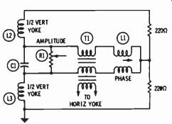
Fig. 40 Top and bottom pincushion correction circuitry.
Fig. 41 Side pincushion correction is accomplished by amplitude modulation
of the horizontal deflection current.
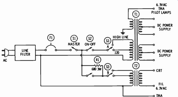
Fig. 42 Schematic of the switching circuitry that permits the CTC40 to take
advantage of the "instant-on" characteristics of semiconductors.
Fig. 43 Three separate rectifier circuits provide the CTC40 with four separate
DC sources.
Power Supply
The CTC40 power supply provides four DC sources for general circuitry requirements and two AC power sources. The AC power sources are for the CRT filaments and pilot lamps.
Power supply switching circuits allow the CTC40 to take advantage of the "instant on" characteristics of solid-state devices. This switching circuitry is illustrated in Fig. 42.
Switching Circuit
AC power is applied through the line filter and circuit breaker to the master power switch, Si. The master power switch applies power through the "instant pic" switch, S2, to both the DC supply transformer, T1, and the CRT filament transformer, T2.
However, when switch S2 is in the "off" position, reduced power is supplied to filament transformer T2 through resistor R1, a 680-ohm, 3 watt component. Using this method, the CRT filament is kept "warm" until full power is applied by closing switch S2. This design insures the full operation of the CTC40 within four to five seconds after turn on.
The master power switch, S1, is a rotary type switch located at the top of the auxiliary consumer-controls bracket. Switch S2 is a pushpull switch located at the top of the consumer-controls panel and is adjacent to the brightness control.
DC Supply Circuitry (Fig. 43)
The DC power supply provides four separate DC sources generated from three separate rectifier circuits.
This is illustrated schematically in Fig. 43.
Rectifiers S1 through X4 are responsible for providing both the 82 and 30-volt sources. The 82-volt supply is derived from the full-wave bridge configuration of rectifiers X1 through X4. The transformer secondary winding that feeds this bridge circuit is center-tapped and is used to feed two of the four rectifiers comprising the bridge network. This forms a full-wave, center-tapped circuit, the output of which is 30 volts.
A second full-wave bridge circuit is comprised of rectifiers X5 through X8. The output of this circuit is the 155-volt source.
The automatic degaussing circuit is coupled to the secondary winding of T1, which feeds rectifiers X5 through X8. This circuit consists of thermistor R1, voltage dependent resistor R2 and degaussing coil L1. Operation of this circuit is the same as that of degaussing circuits previously employed in RCA color chassis.
The 250-volt DC source is obtained from the output of rectifier X9. During normal operation, the CTC40 chassis draws approximately 1.8 amperes of AC current at 120 volts AC input. The average DC current supplied by each leg of the power supply is as follows: 82-volt source-200 ma.
30-volt source-200 ma.
155-volt source-400-700 ma.
(varies with beam current)
250-volt source-50-70 ma.
(varies with beam current)
1st and 2nd Chroma Amplifiers (Fig. 44)
The chroma signal is applied to the base of the first chroma amplifier through a tuned circuit comprised of capacitors C1, C2 and inductor L1. This circuit is referred to as a "chroma take-off" or- "chroma peaker" circuit. Resistors R1 and R2 broaden the bandpass to compensate for loss of chroma side bands on the response curve of the peaker circuit. The ratio of values of resistors R1 and R2 also provide the proper input impedance for the first chroma amplifier.
Bias for the base of the first chroma amplifier stage is supplied and determined by the ACC amplifier. Output of the 1st chroma amplifier, Q1, is RC coupled to the base of the second chroma amplifier, Q2. The 2nd chroma amplifier stage is a straight-forward common-emitter circuit.
Bias for Q2 is obtained from a voltage divider network consisting of resistors R3 and R4. The output (collector) circuit consists of load inductor L2, capacitors C3 and C4, and the capacitance of the coupling cable. This combination of components forms a broadly tuned circuit with a response that falls within the limits of the desired chroma bandpass.
Fig. 44 First stage of two-stage chroma amplifier employed in CTC40 is ACC
controlled.
Fig. 45 Tint control in CTC40 is electrically located in collector circuit
of phase splitter.
Phase Splitter (Fig. 45)
The phase splitter circuitry provides a means of varying the phase of the chroma signal, or, in effect, provides a method of varying the tint. Chroma signals are applied across the color control and capacitance-coupled to the base of the phase splitter. Output voltages are taken from both the collector and emitter and applied across a phase shifting network comprised of the tint control and capacitor C I . The phase splitter and its associated circuitry are located on the customer controls bracket. The tint and color controls are consumer controls and extend through the front control panel.
Bandpass Amplifier (Fig. 46)
The output of the phase splitter is capacitance-coupled through C1 to the base of Q1, the bandpass amplifier. Q1 is connected as a common-emitter. Base bias for Q1 is obtained from the killer stage.
The output load for Q1 is T1, the bandpass transformer.
A negative-going pulse is applied to the base of Q1 for burst blanking. This is done to prevent the color sync signal from being amplified by the bandpass amplifier.
A double-tuned bandpass transformer determines the exact range of chroma frequencies applied to the demodulators. The secondary winding of T1 is shunted and tuned by capacitor C2. Resistor R1 provides loading and aids in determining the "Q" of the circuit.
Burst Amplifier (Fig. 47)
A simplified version of the burst amplifier stage utilized in the CTC40 chassis is illustrated in Fig. 4. The color sync signal from the collector of the second chroma amplifier is applied to the base of the burst amplifier transistor through capacitor C1. A positive-going keying pulse (15 volts p-p) from the horizontal output transformer is applied to the base across resistor R1.
The integrating characteristics of capacitor C1 and resistor R1 provides the required time delay for the keying pulse.
The burst amplifier transistor is keyed into conduction by the pulses from the horizontal output transformer, which arrive at the base of the transistor at the same time as the bursts of color sync signals.
The burst signal is amplified by the burst amplifier and appears across the burst transformer, T1.
Loading for the burst transformer is provided by resistor R2.
During conduction of the burst amplifier, resistor R4 establishes the proper emitter operating point. Capacitor C3 functions as an AC bypass capacitor. Resistor R3 provides the required amount of emitter degeneration for proper amplifier stability with maximum voltage gain. Capacitor C2 *provides the amount of feedback voltage necessary to cancel the effects of the internal feedback capacitance of the transistor.
The burst amplifier base-emitter bias is maintained below cut-off during scan time, or between burst keying pulses. This assures that only color sync signals are supplied to the AFPC detector. The required "scan-time bias" is developed by the discharge of capacitor C3, the emitter bypass capacitor, through emitter resistor R4. Emitter current flow, resulting from the application of the burst keying pulse, places a positive bias on the emitter. This reverse biases the transistor during scan time. Diode X1 functions to prevent the bias voltage from exceeding the reverse emitter-base breakdown voltage rating.
Automatic Frequency and Phase Control (AFPC) Detector (Fig. 48)
The purpose of the AFPC detector circuit is to develop a DC voltage that is proportional to the frequency and phase difference that exists between the applied color sync signal (burst) and the reference signal supplied by the 3.58-MHz oscillator in the receiver. Rigid control over the operation of the 3.58 MHz oscillator is a prerequisite for proper color demodulation. This is because the output of the 3.58-MHz oscillator is the reference, or standard, on which chroma demodulation is based.
Fig. 46 Three signals or voltages are applied to base of bandpass amplifier:
chroma input signal, bias from color killer and negative-going burst signal.
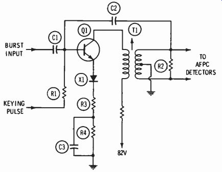
Fig. 47 Simplified schematic diagram of burst amplifier employed in CTC40.
The AFPC detector circuit in the CTC40 chassis is, in effect, a phase sensitive discriminator. The burst signal is fed at equal amplitude and opposite phases through capacitors C1 and C2 to diodes X1 and X2.
A sample of the 3.58-MHz reference voltage is applied to the junction of the cathode of X1 and the anode of X2. When the reference voltage and the burst signal are in phase, the diodes will conduct in equal amounts but in opposite directions. The result is zero AFPC voltage.
If the reference voltage lags the incoming burst voltage, diode X2 conducts more than diode X I , causing an imbalance in current flow through resistors R1-R2, and a positive AFPC voltage will be developed. If the reference voltage leads the incoming burst signal, diode XI conducts more than diode X2, again producing an imbalance in current flow through resistors R1-R2, but in this instance a negative AFPC voltage will be developed.
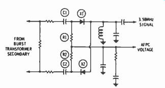
Fig. 48 Automatic frequency and phase control (AFPC) circuit develops DC voltage
proportional to frequency and phase differences between color burst and 3.58-MHz
reference signal.
3.58-MHz Reference Oscillator (Fig. 49)
The chroma reference oscillator is a modified Clapp-type circuit.
Feedback is accomplished by R7, C3, and C2, which couple an in phase signal back to the base.
The operating frequency is determined by the 3.58-MHz crystal and the combined capacitance of capacitors C2, C3 and varactor X1 . The varactor utilizes a specially constructed junction that enhances the normal voltage-dependent capacitance characteristics of a diode.
The frequency of the oscillator can be varied over a very limited range by changing the voltage impressed across the varactor diode. Thus, the AFPC voltage, and the voltage determined by the divider network (AFPC adjust and R3), will vary the oscillator frequency a small amount. Capacitor CI serves as a low-impedance ground return for the varactor and has no effect on the oscillator frequency.
The CW amplifier, Q2, operates into a high-Q, single-tuned transformer, T1, that develops a sine wave from the amplifier output current pulses. Capacitors C6 and C7 function as a capacitance voltage divider network that provides the 3.58-MHz reference level to the AFPC detector circuit. The transformer secondary couples the 3.58 MHz signal to the color demodulator stages.
Color-Killer Circuits (Fig. 50)
The primary purpose of the color killer system is to prevent spurious or extraneous color "noise" from being observed on the CRT during b-w reception. In the RCA CTC40 chassis this is accomplished by cutting off the bandpass amplifier stage.
Control voltage for the color killer is developed by the ACC detector circuitry and is applied to the killer amplifier. The killer amplifier controls the killer switch stage, which, in turn, switches the hand pass amplifier from a state of conduction to a state of non-conduction when a monochrome signal is received.
During periods of color transmissions, the killer switch stage is biased into saturation by the conduction of the killer amplifier. Saturation of the killer switch effectively clamps both its base and emitter elements to the potential of its collector. Since the killer switch is directly coupled to the base of the bandpass amplifier, its collector voltage (as determined by the divider network of R1-R2) determines the forward bias of the bandpass amplifier. This action controls the conduction of the bandpass amplifier which continues to conduct as long as there is a color signal being received.
During monochrome reception the absence of a color sync signal causes the ACC detector to develop a positive output voltage. This positive output signal biases off the killer amplifier and stops the forward biasing current to the killer switch. The killer switch is then cut-off, effectively "opening up" the bandpass amplifier forward bias circuit. With the bandpass amplifier "cut-off," no extraneous chroma information is fed to the color demodulators.
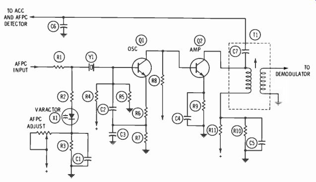
Fig. 49 Modified Clapp-type chroma reference oscillator utilizes regenerative
feedback between emitter and base of Q1 via R7, C3 and C2.
Chroma Demodulators (Fig. 51)
Three color demodulator circuits are employed in the CTC4O chassis, one for each color-difference signal.
The use of a separate G-Y demodulator increases the bandwidth of the signal.
The chroma demodulator circuits are balanced dual-diode detectors.
The output of each dual-diode circuit is proportional to both the phase and amplitude of the applied signal.
Two signals are applied to each demodulator circuit: a composite color signal from the bandpass amplifier and the reference signal from the 3.58-MHz oscillator circuit. The phase of the reference signal is shifted a specific amount with respect to the burst signal for each demodulator, extracting the appropriate color-difference signal from the input chroma signal. Circuit action is as follows: The phase of the 3.58-MHz reference signal applied to the R-Y demodulator is shifted by capacitor CI and inductor L I . This phase shift permits the R-Y demodulator output to be proportional to the amplitude of the R-Y component of the chroma signal. Phase shifting for the B-Y signal is accomplished by capacitor C2 and inductor L2.
The 3.58-MHz reference signal is applied directly to the G-Y component of the chroma signal. Proper loading of the 3.58-MHz CW amplifier is provided by resistors R3 and R4.
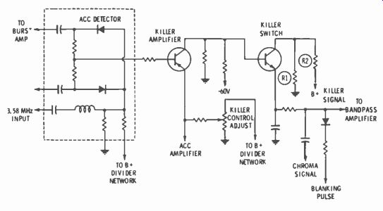
Fig. 50 CTC40 employs two-stage color killer section that controls conduction
of the bandpass amplifier stage.
Fig. 52 Output of chroma demodulators is amplified by two-stage color difference
amplifier. Driver stage is emitter follower for impedance matching between
demodulators and output amplifiers.
Fig. 51 Balanced dual-diode chroma demodulators produce outputs that are proportional
to both the amplitude and phase of the applied chroma signal.
Fig. 53 Clamp diodes in grid circuits of CRT restores DC level of chroma signal
lost in AC coupling between chroma demodulators, chrome amplifiers and CRT
control grids.
Color Driver and Output Circuitry (Fig. 52)
All three color driver and output circuits are identical with the exception of certain component values. For purposes of operational analysis only one circuit, the R-Y driver and output, will be discussed.
The actual theory and operation of the R-Y stage will be representative of all three circuits.
The driver circuit is connected as an emitter-follower to provide the proper impedance match between the comparatively high output impedance of the demodulator circuit and the relatively lower input impedance of the output stage.
The 3.58-MHz ripple component is attenuated from the output of the demodulator circuit by a low-pass filter comprised of inductor L1 and the input impedance of the driver stage. Base bias for the driver stage is developed by the divider network comprised of resistors R1, R2 and R3. A better degree of stability is derived by connecting this network between the collector of the output stage and the base of the driver transistor. RF grounding is provided by capacitor C1, which reduces the effects of output-to-driver feedback capacitance. The gain of the output stage is a function of the emitter resistor R4 and the collector load resistance in the control grid circuitry of the CRT. Clamp Circuitry (Fig. 53)
A certain amount of the chroma DC level is lost because of the AC coupling between the chroma demodulators, chroma amplifiers and CRT control grids. It is the function of the clamp circuit to restore this DC level.
A negative-going 35-volt pulse is coupled from a tap on the horizontal output transformer to the emitter of the clamp transistor, Col. Diode X1 removes positive ripple between pulses, and inductor L1 suppresses any radiation present in the clamp circuitry. Capacitor C1 is used to sharpen the timing of the horizontal pulses. These negative going pulses drive the clamp transistor into saturation. The resulting current flow through the base-emitter junction to ground through resistor RI develops a voltage across resistor R1, and a negative charge on capacitor C2. The charge on C2 allows very sharp turn-off of the clamp transistor at the end of each pulse.
The amplified pulse that appears across the CRT bias control is clamped by zener diode X2, at á level equal to 180 volts below the B+ voltage of 250 volts. A portion of the pulse voltage is fed to a clamp diode, X3, located in each of the three CRT control grid' circuits, resulting in diode conduction, which effectively clamps the CRT control grids to the bias pulse voltage (80 volts). This voltage charges the coupling capacitor, C3, located in the color amplifier output stages.
The DC level resulting from the average DC content of the chroma signal is added to this voltage. Thus, a CRT operating point representing the DC level of chroma information is established.
Tracking
Tracking could be termed as the ability of the CRT to maintain gray-scale throughout the entire brightness range. Proper tracking is accomplished by the development of proper bias levels on the CRT elements, screen grids, control grid, and cathode. The required adjustment procedures of the CTC40 chassis is similar to the procedures used previously in RCA chassis CTC28 and CTC30. Some automatic correction of the potentials on the CRT elements is provided to offset any AC line-voltage fluctuations. Variable voltages for tracking adjustments are derived from the cathode drive controls, the CRT bias adjustment and the screen grid controls. Any fluctuations in AC line voltage is reflected in the B+ potential, and this, in turn, is reflected in the CRT bias and drive voltages. The action of the zener clamp diode, X2 in Fig. 53, causes the CRT bias voltage to vary directly with changes in B+ potentials. This diode action assures that the CRT grids follow the cathodes during changes in zener B+ and, therefore, assures a constant CRT bias with varying line voltages. The CRT screen voltages are obtained from a regulated source and do not vary under line-voltage fluctuations.
Horizontal AFC and Oscillator
The horizontal AFC and oscillator circuitry is illustrated schematically in Fig. 54. The phase splitter stage supplies equal and opposite sync pulses to the familiar dual diode phase detector. Incoming sync pulses are differentiated at the base of the phase-splitter transistor to reduce interference from the vertical sync pulses that are present in the output of the sync separator.
Output pulses from the collector and emitter of the phase splitter are coupled to the phase-detector diodes by capacitors C1 and C2.
A reference voltage taken from the high-voltage transformer is applied to the common diode junction through a waveshaping network.
This network shapes the negative going pulses from the high-voltage transformer into a sawtooth signal that is applied to the AFC circuit.
The frequency of the pulses sampled from the high-voltage transformer is the same as that of the horizontal oscillator.
When the pulses from the high voltage transformer and the incoming horizontal sync pulses occur at the exact same frequency, each diode is keyed into conduction by the sync pulses as the reference voltage passes though zero. The current through each diode will be equal, resulting in equal and opposite charges on capacitors C1 and C2.
As these capacitors discharge through resistors R1 and R2, equal and opposite voltages are developed across the resistors. The voltage at their junction is zero (with respect to ground), and, consequently, the amount of correction voltage developed is zero.
If the horizontal oscillator is running at a frequency less than that of the incoming horizontal sync pulses, a change in the relative position of the reference voltage wave shape during the application of the sync pulses will result. The sync pulses will key the diodes into conduction during the positive portion of the retrace slope; diode X1 will conduct more strongly than diode X2; and the charge on capacitor C1 will become more positive, while the charge on capacitor C2 will become less negative.
Discharge action of these capacitors through resistors R1 and R2 will result in an imbalance of current flow through R1 and R2, and the voltage developed at their junction will go positive. This positive voltage is the correction voltage for the horizontal oscillator and will cause the oscillator to increase in frequency.
Should the oscillator be running at a frequency greater than the incoming sync pulses, a negative correction voltage will be developed at the junction of R1 and R2 as the result of circuit action similar but opposite to that described in the preceding paragraph. Application of the negative correction voltage to the oscillator will produce a decrease in the oscillator frequency.
The DC correction voltage present at the junction of R1 and R2 is fed to an AFC limiting and filtering circuit comprised of diodes X3 and X4, capacitors C3 and C4, and resistor R3. The function of this circuit is two-fold: The limiting diodes prevent the AFC correction voltage from exceeding-O.5V to 0.5 volts; and the filter network prevents the AFC output from being contaminated by unwanted frequencies, such as 60 Hz. (A 60-Hz signal present at this point would result in horizontal bending, twisting, etc.) Horizontal Oscillator A blocking oscillator circuit is employed as the horizontal oscillator in the CTC40 chassis. Basic circuit action is as follows: Voltage pulses present on the collector of the horizontal oscillator transistor are transformer-coupled into the base circuit, driving the stage into cutoff. During the time that the oscillator transistor is cutoff, capacitor C5 discharges through the horizontal hold control circuitry to the "turn-on" potential of the oscillator. The oscillator conducts, a pulse appears at the collector and is coupled to the base, and the cycle repeats.
The settings or adjustments of the horizontal linearity and horizontal hold controls determine the discharge time of capacitor C5 or, in other words, the length of time the transistor remains cut off. In this manner the horizontal hold control determines the frequency of the horizontal oscillator.
This is accomplished by adding the correction voltage from the AFC circuit to the charge capacitor C5.
This correction voltage, depending on its polarity and amplitude, will either add or subtract from the charge on capacitor C5, which, in turn, either increases or decreases the time required to discharge C5 to the turn-on potential of the oscillator. This circuit action alters the frequency and phase of the oscillator in accordance with the broadcast sync pulse.
Horizontal Oscillator B + Source
A special 30-volt source is used to supply B+ to the horizontal oscillator. This is done to assure that the horizontal oscillator will be capable of supplying adequate drive to the horizontal output stage at the instant power is first applied to the receiver. The filter circuit of the normal +30-volt supply source requires too much time to reach full value; therefore, the special circuit, comprised of X5 (zener diode) and resistor R4, is used to develop the required 30 volts from the more lightly filtered 155-volt source. This circuit functions to reduce the time required for the oscillator output to reach its normal operating level.
Horizontal Output Circuitry
It is necessary to slightly alter the shape of the horizontal oscillator output waveform to minimize the possibility of pre-triggering the commutator switch. This is accomplished by the waveshaping network composed of diode X5, capacitor C6 and resistors R5 and R6.
---------Fig. 54 Schematic diagram of horizontal AFC and horizontal oscillator
circuitry employed in RCA CTC40 chassis.
-----------
The voltage developed across the output winding of the horizontal blocking oscillator transformer is coupled to this waveshaping network. R6 and C6 function as a differentiating network, producing a positive voltage spike to turn on the commutator switch. The diode, X6, is reverse biased during the negative-going portion of the output voltage waveshape. This permits capacitor C6 to discharge through the parallel paths provided by RS and R6. This discharging action holds the waveshape negative until the next positive pulse arrives. Thus, the commutator gate is held negative during trace-time, reducing commutator pre-triggering.
Control of Temperature Induced Frequency Change
It is an inherent characteristic of transistors that their operation will vary with changes in ambient and internal temperature. A thermistor, RT, in conjunction with resistor R7, functions as a temperature-sensitive, voltage-divider network. As the temperature of the horizontal oscillator transistor changes, its operating frequency tends to change.
The same changes in temperature that affect the transistor also affect the thermistor (RT). The transistor base-circuit voltage will be altered by the temperature-induced changes in the divider network comprised of RT and R7. This change in base circuit voltage will be in a direction that will cancel out the effects of temperature on the transistor.
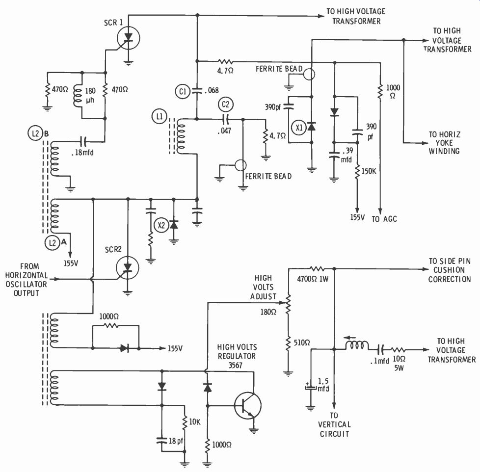
Fig. 55 Partial schematic diagram of horizontal output circuitry found in
CTC40.
Horizontal Deflection
The RCA CTC40 chassis utilizes two silicon-controlled rectifiers (SRC's) and their associated components to generate the necessary yoke current and fulfill high-voltage requirements.
The function of any horizontal deflection system used in television receivers utilizing electromagnetic deflection is to provide a linear flow of current through the yoke windings which, in turn, moves an electron beam from one side of the picture tube screen to the other in a linear sweep. This action is normally referred to as "trace", and the yoke current that caused the deflection is called "trace current." Trace current must be in sync with the incoming TV signal. The yoke current must also provide a means of returning the CRT beam to the starting side of the CRT screen. The current that accomplishes this is referred to as retrace, or flyback, current.
Circuit Action
A partial schematic of the horizontal output circuit is shown in Fig. 55. Diode X1 and silicon-controlled rectifier SCR I control the flow of current through the horizontal yoke windings during the CRT beam trace time. Diode X2 and silicon-controlled rectifier SCR2 control the flow of current through the horizontal yoke windings during retrace time.
Energy storage and timing properties are provided in the circuit by components L1, C1 , C2 and Cy.
Inductors L2A and L2B provide a charge path for 1.1 and C1, and a gating, or keying, signal to SCR1.
The complete horizontal-deflection yoke-current cycle can be divided into a sequence of individual actions involving different modes of horizontal circuit operation. These actions are accomplished during discrete intervals of the horizontal deflection yoke current cycle.
During the first one half of CRT beam trace time, the current through the horizontal deflection coils decreases towards zero and flows through trace diode X1, resulting in a charge build-up on capacitor Cy.
During this interval (first half of trace time), silicon controlled rectifier SR1 the trace SCR, is prepared for conduction by the application of the proper gate-voltage pulse.
However, the SCR1 will not conduct until its anode/cathode junction is forward biased. This condition will be satisfied during the second half of the beam trace cycle.
At the end of the first half of trace, yoke current reaches zero, capacitor Cy starts discharging through the yoke inductance, and the current flow through the circuit reverses, reverse-biasing diode X1 and, simultaneously, forward biasing the SCR1. The capacitor discharges into the yoke inductance through SCR 1 and the resulting yoke current completes the second half of trace.
When the second half of trace is concluded, the CRT beam has scanned across the entire width of the CRT screen. At this point, a pulse, derived from the horizontal oscillator circuit, keys the retrace SCR into conduction. This action releases the charge previously built up, or stored, on capacitor Cy, and current flows into the commutator circuit comprised of inductor L1 and capacitor C1.
Because of heavy forward current flow through the yoke circuit (SCR1, Ly and Cy), the net current resulting from the combined circuit actions of the commutating switch circuit and the yoke circuit continues to allow the trace rectifier, SCR1, to conduct.
At this point both rectifiers, SCRI and SCR2, are conducting. However, the current flowing in the commutator circuit increases much more rapidly than the current flow in the yoke circuit. After an extremely short period of time (two to three microseconds) the net current flowing in SCR1 reverses, turning off SCR I at the start of retrace.
Circuit conditions are now set to initiate retrace: Trace rectifier SCR1, along with diode X1, is cut off, and retrace rectifier SCR2 is conducting. The result is a series resonant circuit comprised of inductor L1, capacitor C1 and the horizontal yoke windings. (Capacitor Cy is also in series with these components, but, because of its value, can be disregarded.)
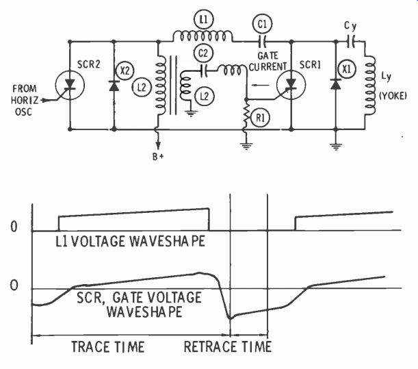
Fig. 56 Simplified schematic of horizontal output circuit, and diagram showing
instantaneous voltages across L1 and SCR1 during trace and retrace times.
The current through this circuit causes the CRT beam to retrace half way across the screen. At this point the current flow has decreased to zero. Current flow in the series resonant circuit now reverses, and retrace rectifier SCR2 ceases conduction because the current flow in the circuit is opposite the normal flow of forward current.
Diode X2 is now forward-biased by this reversal of current and starts conducting, supplying the energy for the remainder of retrace. The energy previously stored on capacitor C1 has been returned to the yoke inductance.
Retrace current flowing in the horizontal yoke winding returns the electron beam to its starting point.
The time interval of yoke retrace current flow is made equal to the desired retrace time by selection of the proper values of components L1, C1 and Ly.
These components are selected to be resonant at a frequency which has a period equal to two times the retrace time interval. Therefore, the current flowing during one half cycle of circuit oscillations will accomplish the full retrace function.
After completion of one full cycle (trace and retrace), the circuit must be made ready for the next cycle.
This includes restoring energy to the commutator circuit and resetting the trace rectifier, SCR1. Both of these functions are performed by utilizing circuitry which includes inductor L2.
During retrace, inductor L2 is connected between B+ and ground by the conduction of SCR2 and diode X2, respectively. When X2 ceases conduction, inductor L2 is removed from ground. A charge is built up on C1 from the B+ line through inductor L2. This charging process continues throughout the trace interval, until retrace begins.
The charge on C1 serves to replenish energy to the yoke circuit during the retrace interval.
The voltage developed across inductor L2 during the charging of capacitor C1 is used to forward-bias the gate of SCR1. This sets up SCRI and enables it to conduct upon receiving the proper signal.
The voltage developed across inductor L2 is coupled to the gate of SCR1 via L2A, C2 and R 1.
These components form a wave shaping network that forms a pulse with the proper shape and amplitude to enable SCR1 to conduct when its anode/cathode junction is forward-biased. This will occur approximately mid-way through the trace interval.
This concludes our analysis of RCA's solid-state CTC40 color chassis. (Schematic diagrams used in this Section courtesy of RCA.)
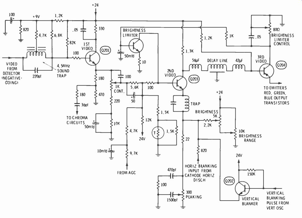
Fig. 57 Transistorized "Y" channel with brightness limiter and vertical
blanking transistors is used in new Zenith chassis.
Zenith's 12B14C50 Color TV Chassis
The new Zenith 12B14C50 color TV chassis employs more transistors than any previous Zenith color chassis. It is equipped with 14 transistors and 12 tubes, and a fully transistorized "Y" channel.
The color and the "Y" signal are pre-mixed and applied to the cathodes of the CRT, permitting the CRT control grids, to be returned to a fixed DC source.
As in an earlier color chassis, the 2nd color amplifier and the color demodulator integrated circuitry is contained in a plug-in module which can be removed and replaced from the top of the chassis.
Zenith uses a ganged contrast and color control, which they call a "color commander." To maintain the correct black level with a change in contrast, a special "black tracking" circuit increases or de= creases the brightness slightly as the Contrast/Color control is rotated.
The chassis also is equipped with a simplified automatic degausser circuit, a new high-level noise clipper; a simplified focus circuit, a pincushion circuit using a saturable reactor, and an "automatic" tint control circuit.
The Video (Y) Amplifiers
The "Y" channel in the 12B14-050 chassis is all transistorized, as shown in Fig. 57. There is an emit follower 1st video amplifier, a common-emitter 2nd video amplifier, and an emitter-follower 3rd video amplifier. The 3rd video amplifier also serves as an impedance matcher and "modulator" to the emitters of the red, green, and blue output transistors.
The contrast control is in the emitter circuit of the 1st video; the chroma take-off also is in this circuit. The brightness and brightness range controls are in the emitter circuit of the 2nd video. Vertical and horizontal blanking also is inserted at the 2nd video emitter.
Stabilization from three sources is applied at the base of the 2nd video transistor, Q203.
-----------
Setting the Brightness Range and Brightness Limiter
To get full effectiveness from the Brightness Limiter circuit it must be adjusted in conjunction with the Brightness Range control as follows:
1. Turn the Brightness Limiter control fully clockwise.
2. Turn Brightness control fully clockwise.
3. Adjust Brightness Range until picture blooms 1 inch.
4. Adjust Brightness Limiter counterclockwise until picture blooms only 1/4 inch.
----------
1st Video Stage
The video signal from the detector diode is fed through peaking coils and a sound trap to the base of the 1st video, Q201. At first glance, the resistors in the base circuit of 0201 appear to comprise a rather complex DC biasing network.
The reason for this many resistors, according to Zenith, is to provide a better AC match between the medium-high output impedance of the diode detector and the medium low input impedance of the 1st video transistor. As far as the DC bias is concerned, the resistors are in parallel. The 4.7K-ohm resistor helps sharpen the tuning of the trap.
The contrast control circuit parallels the 180- and 470-ohm emitter resistors and varies the AC video signal level fed to the base of the 2nd video amplifier, Q203.
The "black-tracking" circuit operates because of the different AC and DC impedances of the contrast control circuit. For video (AC), the circuit offers an impedance of 1220 ohms (the 1 k contrast control and the 220-ohm resistor in series with it, disregarding the 180and 470 ohm parallel resistors) because AC is bypassed around the 10k resistor by a 50-mfd capacitor. For DC, however, the 50-mfd capacitor has no effect, so the circuit impedance is 11,220 ohms. Consequently, with the contrast control arm at the low end, the signal level is reduced about 51/2 times, but the DC bias level (affecting the brightness) is reduced only about 1/11. In other words, lowering the contrast also slightly lowers the brightness, while increasing the contrast slightly increases the brightness, both actions keeping the CRT black level relatively constant.
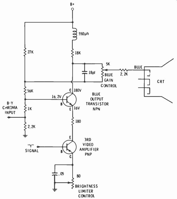
Fig. 58 Simplified schematic of pre-CRT mixing of chroma and "Y" signals.
The 2nd Video
With direct-coupling between video stages, which is used in most color sets, a change in bias in any stage causes a corresponding change in picture tube brightness. This is why brightness problems in color sets often occur in the video amplifiers, and why the brightness control and brightness range can be inserted at almost any convenient spot in the circuit following the chroma takeoff and contrast control.
But there are some disadvantages to the direct-coupled circuit. If, during warmup, the current flow through one or more of the transistors changes, the brightness also will change. To compensate for warmup change in this circuit, a negative-temperature-coefficient (decreases in resistance with increase in heat) thermistor is placed in the base bias circuit of the 2nd video stage. As the transistor heats it tends to draw more current, but the thermistor compensates by reducing the DC bias to the base, which in turn, reduces the conduction of the transistor circuit.
Another problem in direct coupled circuits is that when weak signals are received the detector output drops below the normal level maintained by the AGC on stronger signals. This means that the brightness would increase on weak signals. To prevent this, the base of the 2nd video amplifier is tied through an RC network to the AGC line. Because the AGC line goes more negative when a weak signal is received, more negative voltage is applied to the base of the 2nd video, preventing a drastic change of brightness.
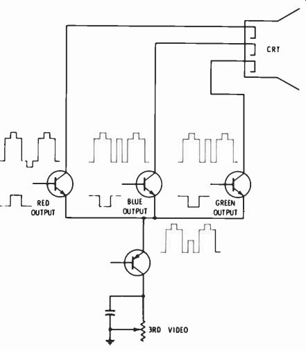
Fig. 59 Simplified circuit showing matrixing of chroma signals with the "Y" signal
when a red color bar is being received.
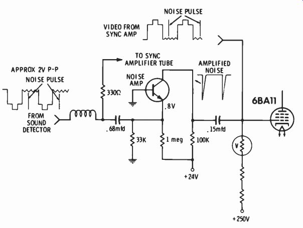
Fig. 60 Common-base, high-level noise amplifier used in new Zenith chassis.
During normal reception, video input signals are not strong enough to override
the bias of the noise amplifier transistor; however, a strong noise pulse will
cause it to conduct and apply a strong negative pulse to the 6BA11 grid.
A third stabilizing signal is introduced at the base of the 2nd video by the brightness limiter transistor; this application will be discussed in detail later in this article.
Located in the emitter circuit of the 2nd video amplifier arc another trap, a peaking control circuit, input for vertical and horizontal blanking signals, and the brightness and brightness range controls.
The peaking control functions by varying the frequency response of the video amplifier. When the arm of the peaking control is at the "hot" end, the higher video frequencies arc bypassed around the major portion of the emitter resistance, producing maximum high frequency gain and pictures with sharp outlines but more apparent noise and snow, especially in weak signal areas. With the peaking control arm at the "ground" end, the high-frequency gain is reduced and the outlines in the picture tend to smear, but noise and snow are less apparent. The peaking control is a "customer preference" control and operates on the same principle as a tone control in an audio circuit.
"Normal" operation is with the control at about midrange.
The brightness and brightness range controls vary the emitter bias of the 2nd video and, in turn, this change in bias is projected through the remainder of the video stages to the cathodes of the CRT. Brightness is minimum when the arm of the brightness control is at the +24 volt side. For this reason, the brightness control can always vary the brightness to zero regardless of the setting of the brightness range control. The brightness range varies the amount of positive voltage on the "low" side of brightness control and sets the maximum level to which the customer can increase the brightness.
Horizontal blanking also is inserted at the emitter of 0203, through an 820-ohm resistor which is tied to the cathode of the horizontal discharge tube.
Vertical blanking is applied at the same point, but the vertical pulses, taken off the vertical oscillator-amplifier, are first fed to a vertical blanker transistor to reduce the loading and provide a better impedance match.
3rd Video Stage
The output of the 2nd video amplifier is fed through the delay line to the base of the 3rd video. There is an 80-ohm adjustable resistor in series between the 3rd video collector and ground. This is the brightness limiter control. The positive voltage developed across this control is filtered to remove video, and the resultant DC then is fed to the base of the NPN brightness limiter transistor. This positive voltage causes the transistor to conduct and supply a negative voltage to the base of the 2nd video amplifier.
The operation of this two-stage compensating circuit is as follows: If the current through the 3rd video transistor increases for any reason, there will be additional positive voltage applied to the base of the brightness limiter, which will increase the negative bias on the 2nd video, which, in turn, will reduce the bias on the 3rd video, almost completely cancelling an increase of current in the 3rd video.
The opposite condition occurs if the 3rd video transistor current should drop for any reason. In other words, this is an amplified stabilizing circuit that limits extreme changes in bias, thereby limiting undesirable brightness changes.
Pre-CRT Matrixing
Before increased use of transistors, almost all manufacturers mixed (matrixed) the video and chroma signals in the picture tube by applying the video to the CRT cathodes and the color to the CRT grids.
This had the disadvantages of requiring high-level color amplifiers and the possibility of tracking problems in either or both the video and color amplifier circuits.
By pre-mixing the video (Y) and the color, the final video amplifiers can amplify both the video and the color, and the CRT grids can be returned to a fixed DC source, reducing the possibilities of tracking errors.
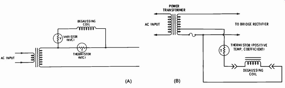
Fig. 61 (A) More conventional degaussing circuits have employed at least two
voltage and/or temperature sensitive resistors. Zenith automatic degaussing
circuit (B) uses only one thermistor, and it has a positive temperature coefficient.
Fig. 58 shows how the video and one color signal are mixed in this chassis. The "Y" signal is fed into the 3rd video amplifier, which is in series with the emitter of the B-Y (blue) output transistor. This, in effect, mixes the two signals so that a composite of the two appears at the collector of the blue output transistor, where it is coupled through the blue gain control to the blue cathode of the CRT. Fig. 59 shows, in simplified form, how this pre-CRT mixing occurs.
Suppose a red bar is being transmitted. The bar will appear gray on a black-and-white set because the video signal is about "half way to black", as can be seen by the waveform at the emitter of the 3rd video amplifier. With no color input to any of the output transistors, there . will be an exact replica of this signal (except amplified) at all three output collectors. (Remember, there is no phase inversion because the input is to the emitters.) But, with a red signal coming from the color demodulator, there is a positive pulse at the base of the red output transistor. This positive pulse causes the collector to go negative (phase is inverted between base and collector), making the red CRT cathode also go negative, which, in turn, increases the brightness of the red gun. At the same time the positive pulse is arriving at the red output transistor, the color demodulator is supplying negative pulses to the basis of the green and blue output transistors, which produces positive-going signals on their collectors and on the blue and green CRT cathodes, decreasing to zero the brightness of these two colors.
The same process occurs if a blue or green bar were transmitted, except that the corresponding output transistor would receive the "turn on" signal and the other two the "turn off" signal from the chroma demodulator.
The Noise Clipper
A new high-level noise canceller is used in this chassis. As shown in Fig. 60, the transistor is in a common-base circuit designed to feed high-level negative noise pulses to the 1st grid of the 6BA 11 sync tube. During normal operation the video input to the noise amplifier transistor is insufficient to overcome the reverse bias between its base and emitter, and, consequently, there is no transistor output to the grid of the 6BA 11. However, when a strong noise pulse occurs, it overrides the transistor reverse bias and appears as an amplified negative pulse at the grid of the sync tube.
(There is no phase change between input and output of a common-base amplifier.) This amplified negative pulse cancels the effect of the positive-polarity noise pulse, which also is fed through normal channels to the other input grid of the 6BA 11.
This prevents the noise pulse from falsely triggering either sweep circuit.
The Automatic Degaussing Circuit
Most automatic degaussing circuits employed previously use at least two self-variable resistors, either varistors or thermistors or a combination of the two, such as the design shown in Fig. 61A. In this circuit both control units have negative coefficients.
When power is first applied to the set and the thermistor is "cold", its resistance is relatively high, about 120 ohms. Consequently, maximum voltage is developed across it. At the same time, the resistance of the varistor is at minimum, which permits maximum 'current flow through the degaussing coil.
As the set warms up, the resistance of the thermistor decreases, finally reaching about 2 or 3 ohms.
The voltage drop across it also decreases, which, in turn, causes the resistance of the varistor to increase to maximum, cutting off almost all current flow through the degaussing coil.
The automatic degaussing circuit in Zenith's new chassis uses a low voltage, high-current degausser and a single thermistor with a positive temperature coefficient. When the set first is turned on, the thermistor is cold, its resistance is at minimum, and about 6 amps of current flow through the degaussing coil. During the first few seconds of operation, the resistance of the thermistor increases to maximum and current through the degaussing coil decreases to about 30ma, which is low enough not to affect the picture tube, yet sufficiently high to keep the thermistor warm enough to maintain a high resistance.
The Focus Circuit
The focus circuit in the new Zenith chassis, shown in Fig. 62, is simply a voltage divider network connected directly to the 25KV high-voltage source for the CRT. By placing the control in the "tail", or "cold", end of the circuit, the voltage on the control is kept at a reasonable level, and the danger of arc-over or shock is minimized.
Pincushion Correction
Another change in the new Zenith chassis is the deletion of the pincushion amplifier tube. A saturable reactor is used instead-not a new idea, but one that Zenith has not used before.
Fig. 62 Resistive-divider focus circuit eliminates the need for a focus rectifier.
The saturable reactor uses two separate windings on a special core material. One of the windings is in toroidal form (Fig. 63A), which has no air gap and, because it keeps all the lines of force within the core itself, needs no shielding-it does not radiate nor does it accept electromagnetic signals not directly induced into the core by another toroidal winding on the same core. However, because the core has no air gap, it does saturate rather easily with medium current. With low current in the coil, the coil has a high inductance and reactance. But as the coil current increases, the inductance and the reactance decrease, and once the core has saturated there is little reactance to current variations in the coil.
The second winding of this pincushion unit is wound in normal fashion on the same core as the first winding (Fig. 63B). Because the two windings are at a 90-degree angle to one another, there is no transfer of voltage between the two; however, because the core is common to both windings, the second winding can vary the reactance of the first winding by causing core saturation.
Utilizing this effect, the signal applied to the toroidal coil can be modulated by the signal applied to the second winding, but the second winding will not be modulated by the signal in the toroidal winding.
For correction of pincushion at the top and bottom of the screen, the vertical signal is applied to the toroidal coil, and the horizontal signal is applied to the normal coil.
The vertical signal then is modulated by the horizontal signal, but the vertical signal does not affect the horizontal because, as far as the normally wound coil is concerned, its core has a large air gap and never saturates.
In this particular reactor it requires current flow in both the vertical and horizontal circuits to saturate the core.
Here's how it works: At the beginning of the vertical sweep (top of raster), the sawtooth of current is at its highest amplitude, and this current, plus the current of the top horizontal line, produces maximum saturation of the reactor, which produces minimum reactance and maximum vertical current flow. Because the current is maximum at the beginning and end of each horizontal line, there would be maximum vertical deflection at the ends of the lines-which is just opposite the effect needed. To correct for this, a secondary winding tunable around 15,750 Hz is provided. By adjusting the winding, the phase can be shifted to produce maximum vertical deflection at the center of the screen, instead of at the ends of the lines.
As the beam sweeps downward across the CRT, the vertical yoke current decreases at a linear rate, decreasing the saturation and increasing the reactance of the coil, so that no correction occurs at the center of the screen. As the current increases again to sweep the beam on down to the bottom, the saturation again occurs, producing maximum vertical sweep at the center of the raster.
"Automatic" Tint Control By pulling out the tint control knob on this Zenith chassis the customer can have "automatic" tint.
The control functions by shifting the demodulation angle from the normal 105 degrees to 132 degrees. This shifts the R-Y (red) more toward orange, and there is less apparent flesh tone change as the set is switched from channel to channel.
Fig. 64 shows how the automatic tint control circuit functions. The phase of the 3.58 oscillator injection to the color demodulator is changed by switching in a simple phase shifting network so that the demodulation angle is changed by about 27 degrees.
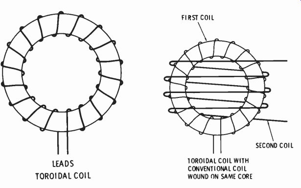
Fig. 63 (A) Toroidal coil. (B) Toroidal coil with a conventional coil wound
on same core. There is no electromagnetic transfer of energy between the two
coils, but current in the conventional coil can cause core saturation and a
reduction in reactance of the toroidal coll.
Fig. 64 Changing the 3.58 oscillator injection phase angle at the input. of
the color demodulator by about 27 degrees shifts the R-Y (red) signal toward
orange, so there is less apparent flesh tore change when the set is switched
from channel to channel.