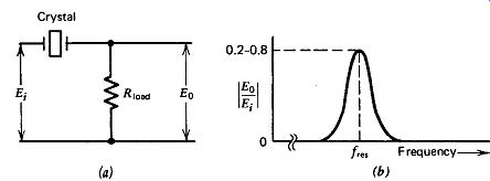
Figure 3.1. Typical crystal series connection: (a) circuit and (b) circuit gain versus frequency.
| Home | Audio mag. | Stereo Review mag. | High Fidelity mag. | AE/AA mag. |
3.1. OSCILLATION
A circuit will oscillate if it has positive feedback and a loop gain greater than 1. With a crystal as a series element in the loop and no other frequency-sensitive elements in the circuit, it will oscillate at the crystal's fundamental series-resonant frequency. A quartz crystal always wants to oscillate at its fundamental frequency and must be forced to oscillate at a harmonic.
When the oscillator circuit's feedback loop is first closed, sine wave oscillation begins, and the amplitude increases until overload occurs.
The waveform at overload becomes a clipped sine wave and finally approaches a square wave at heavy overload. Crystal oscillators can usually provide either a square wave or a sine wave output. The signal driving the crystal is most often a square wave, and the signal out of the crystal is always a sine wave. Either waveform can be used for an output by tapping the appropriate point in the circuit.
3.2. SERIES RESONANCE VERSUS PARALLEL RESONANCE
There is no such thing as a parallel-resonant crystal oscillator. All crystal oscillators operate either at or near (above or below) series resonance.
What is usually meant by parallel resonance is that the crystal has a high load impedance across its terminals. This is in contrast to series resonance, which usually means that the crystal has a low load impedance across its terminals. Series resonance physically exists in the crystal, but parallel resonance exists only as a crystal measurement phenomenon.
When the impedance of a crystal is measured externally as a function of frequency, an impedance peak will be found above series resonance, where part of the crystal's motional inductance L, parallel resonates with the crystal's shunt terminal capacitance Co.
From a circuit viewpoint, the crystal's shunt terminal capacitance C, should be considered as part of the external load on the crystal and not as part of its internal frequency-controlling L, and C, elements. Experimental data confirming this viewpoint are given later. When parallel resonance is mentioned in this guide, it will have the usual meaning that the crystal has a high load impedance across its terminals, and not that the crystal is oscillating at the higher frequency where the crystal's input impedance peak occurs.
3.3 BASIC CRYSTAL CIRCUIT CONNECTIONS
Figure 3.1. Typical crystal series connection: (a) circuit and (b) circuit
gain versus frequency.
How should a quartz crystal be connected in an oscillator circuit? What load impedance should it see? These are key questions in the design of an oscillator circuit. For a crystal to control the frequency of an oscillator circuit, the crystal must maximize the oscillator's gain at the oscillation frequency and minimize it at all other frequencies. It is well-known that a crystal's impedance goes to a minimum at series resonance and to a maximum at parallel resonance. The design question is how best to take advantage of this and give the crystal maximum control of the oscillation frequency.
One approach is to connect the crystal as a series element in the oscillator circuit, as shown in Fig. 3.1. The crystal acts as part of a voltage divider with the resistor R_load and operates at series resonance with zero phase shift through the voltage divider. The gain 1 Eo/Ei 1 through the
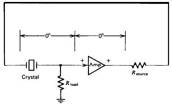
Figure 3.2. Typical series oscillator circuit, voltage divider reaches a maximum
of something less than 1.0 at series resonance, as shown in Fig. 3.1.
Figure 3.2 shows a typical oscillator circuit using the crystal as a series element. To give the crystal maximum control of the loop gain, the crystal must have maximum control of the voltage divider, which means that both the source and load resistances shown in Fig. 3.2 should be small with respect to the crystal's impedance at series resonance; that is, they should be smaller than the internal series resistance R, of the crystal.
An alternative way of looking at the series circuit in Fig. 3.2 is that the amplifier's output puts a voltage across the crystal, and the amplifier's input samples the current through the crystal, which is a maximum at series resonance. Again, the crystal will have maximum control of the loop gain when both Resource and R_load are small with respect to the crystal's internal series resistance R,.
Another design approach is to connect the crystal as a shunt element, as shown in Fig. 3.3. The crystal is again part of a voltage divider. Here, the voltage divider's series element has to be a capacitor or inductor and cannot be a resistor. Figure 3.3 shows a capacitor C, as the series element of the voltage divider. Putting the capacitor C, in series with the crystal raises the oscillation frequency slightly above the crystal's series-resonance frequency. The voltage divider's gain 1 &,/Ei 1 at the oscillation frequency peaks at about 10-15X, as shown in Fig. 3.3, because the circuit resonates at this frequency. There is a 90 degr. phase lead through the voltage divider at the oscillation frequency at the peak of the gain curve. To use this shunt network in an oscillator circuit requires adding another 90 degr. phase-lead (or lag) network into the circuit.
Figure 3.4 shows a shunt oscillator circuit with a 90 degr. phase-lead net work, using the inductor L and the amplifier's output resistance R,,, to provide the phase lead. This is the Miller circuit.
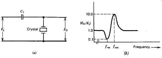
Figure 3.3. Typical crystal shunt connection: (a) circuit and (b) circuit
gain versus frequency.
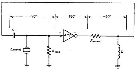
Figure 3.4. Typical shunt oscillator circuit, with 90 degr. lead network (Miller).
Figure 3.5 shows a shunt oscillator circuit with a 90 degr. phase-lag net work, using a shunt capacitor C, and the amplifier's output resistance R_s degr to provide the phase lag. This is the Colpitts circuit. Note that the phase-lead network requires using an inverting amplifier, while the phase-lag network requires a noninverting amplifier. The crystal's load resistance R_l, must be high in both Figs. 3.4 and 3.5 to give the crystal maximum control of the voltage divider's gain.
In actual practice, the phase-lead and lag networks used in shunt circuits generate a little less than 90 degr. of phase shift. This does not matter because the circuit's oscillation frequency will simply move slightly off the amplitude peak shown in Fig. 3.3, changing the phase shift through the voltage divider enough to compensate for the less-than-9 0 degr. phase shift of the lead and lag networks.
The need for low load and source resistances on the crystal for series operation and a high load resistance on the crystal for shunt operation is typical of crystal oscillator circuits. How low and how high these resistances should be to give good in-circuit Q is an important design parameter that affects the circuits' short-term frequency stability. This subject is discussed in detail in Sections 4.2, 6.1, and 6.2.
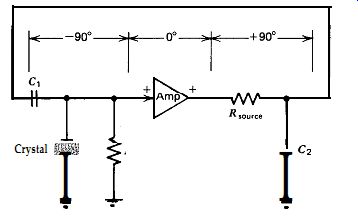
Figure 3.5. Typical shunt oscillator circuit, with 90 degr. lag network (Colpitts).
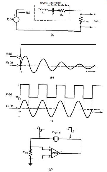
Figure 3.6. Crystal response to a square wave drive.
3.4. CRYSTAL RESPONSE TO A STEP INPUT
What happens to a crystal when it is driven by a square wave? Most series-resonant oscillator circuits put a square wave of voltage across the crystal and sample the current through the crystal by means of a resistor in series with it. The current signal is then fed into the amplifier input.
The relationship between the voltage across the crystal and the current through it is important for understanding how the series-resonant oscillator circuit works. This can be understood by first looking at how the crystal responds to a step input and then extending this to a periodically reversing step input; that is, a square wave.
A simplified equivalent circuit for the crystal at its fundamental series resonance is the series RLC network, as shown in Fig. 3.6a. The crystal's shunt terminal capacitance CO is ignored here. A current-sampling resistor R_ext is added in series with the crystal, and the crystal is driven by a step input of voltage Ei. For simplicity, the two series resistors R, and R ext are combined into one R. The relationship between the applied voltage and resulting crystal current is given by the Laplace transform,
For a voltage step input,
Using the inverse transform, the transient solution for the voltage across R,,. is output:
E, (t) = i (t)&* = . Rexte-t'(2RL) sin [v/c/L - I/(4R2L2) t] VCIL - 1/(4R2L2)
The significance of this equation is that the current through the crystal is a (damped) sine wave and phased so that its starting point at the 0 degr. phase-angle position is time coincident with the start of the step input, as shown in Fig. 3.G. If the step input is reversed (i.e., dropped back to zero) every time the current sine wave goes to zero at 180 degr. and 360 degr., the exponential decay term drops out, and the transient solution becomes the steady-state solution. The phase relationship between the input square wave of voltage and the output sine wave of current then be comes as shown in Fig. 3.6~. Note that there is no phase shift between them.
If the sine wave of crystal current is fed into an amplifier with enough gain so that the amplifier output saturates and makes a square wave out of the sine wave and if this square wave is used to drive the crystal as shown in Fig. 3.6d, then conditions for a periodically reversed step input are obtained, and there is continuous oscillation in the crystal. If the crystal and its amplifier circuit are actually built as shown in Fig. 3.6d, the sine and square wave waveforms observed will be seen to have the same polarity and phasing as shown in Fig. 3.6. This concept of zero phase shift between the crystal's square wave input and its sine wave output underlies the operation of the series-resonant oscillator circuit.