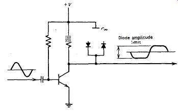
Figure 4.1. Diode amplitude clamp.
| Home | Audio mag. | Stereo Review mag. | High Fidelity mag. | AE/AA mag. |
The most ,important parameters in designing a crystal oscillator circuit are:
1. Crystal's internal series resistance R,.
2. Load impedance across the crystal terminals.
3. Oscillator's loop gain.
4. Reduced crystal voltage limits above 1 MHz.
5. DC biasing of the transistor and IC amplifier stages.
6. Transistor's high-frequency gain limit f,.
Note that three of the six circuit design parameters are crystal related.
Each of these parameters is discussed in the following sections.
4.1. CRYSTAL'S INTERNAL SERIES RESISTANCE R_S
The design of an oscillator circuit is overwhelmingly dominated by the crystal's internal series resistance R_s--far more than by any other parameter. A crystal's series resistance R, varies from a low of 10 s1 at 20 MHz to 200,000 ohm at 1 kHz. The problem comes in providing the wide range in load resistance required to match the wide range in the crystal's series resistance R_s. For series resonance, the crystal's load resistance is usually set equal to or somewhat less than the crystal's internal series resistance R_S in order to get good in-circuit Q. For parallel resonance, the load resistance has to be much higher, up to 500 M-ohm at 1 kHz, to get good in-circuit Q.
Considerable variation in circuit design is required to provide such a wide variation in the crystal's load resistance. At high frequencies, emitter follower outputs will provide low-resistance sources and loads.
At medium frequencies, transistor bases and collectors, FET source follower outputs, and FET drains will all provide medium-resistance sources and loads. And at low frequencies, FET gates will provide high resistance loads. The gain of a FET amplifier stage is about an order of magnitude less than that of a bipolar transistor stage, so that a second amplifier stage is usually required whenever a FET is used.
4.2. LOAD IMPEDANCE ACROSS THE CRYSTAL TERMINALS
The external load tied across the crystal terminals has a considerable effect on the crystal's frequency and its frequency stability. The oscillation current through the crystal's internal frequency-controlling elements Lx and Cx passes out of and back into the crystal through the crystal terminals. The crystal is driven by putting a voltage source in series with this current loop. The resulting current through the crystal's frequency-controlling elements is measured by sampling the voltage drop across a series element in the loop.
Ignoring the crystal's shunt terminal capacitance C_0 putting an inductor or capacitor in series with the crystal's terminals will put the inductor or capacitor in series with the current flowing through the crystal's internal frequency-controlling elements LxCx. This changes the total net series inductance or capacitance in the current loop and the loop's resonant frequency. Putting a small variable capacitor in series in this loop is a common method of trimming oscillator frequency. Whether or not the crystal's shunt terminal capacitance Co can be ignored depends, of course, on the relative impedance of the series inductor or capacitor with respect to the impedance of C_0.
If a low-impedance load is used across the crystal terminals, the circuit is called series resonant. This low impedance has to include the complete external circuit impedance seen by the crystal, looking at the circuit from the crystal terminals. This includes the output resistance of the drive amplifier, the current-sampling load resistor, and the input resistance of the amplifier's input.
If a high load impedance is used across the crystal terminals, the circuit is called parallel resonant. The crystal has a shunt terminal capacitance Co of its own, amounting to 3-15 pF. This shunt terminal capacitance Co is part of the external load on the crystal as far as the crystal's internal frequency-controlling elements L, and C, are concerned. The impedance of Co normally defines the highest load impedance that can be put across the crystal terminals, although at high frequencies (above 50-70 MHz), it is parallel resonated with an inductor to remove it from the circuit.
Tying a resistive load R_load across the crystal terminals gives a total paralleled RC load of R_load and Co across the crystal's frequency controlling elements L, C,. To determine loading effects on the crystal, it is convenient to convert this paralleled RC load combination to its equivalent series values of R_series and C_series. The load the crystal wants to see is the smallest possible equivalent series load resistance &ties, since this resistance reduces both the in-circuit Q and short-term frequency stability. In practice, if good oscillator performance is to be obtained, the equivalent series load resistance Z_series should be made equal to or somewhat less than the crystal's internal series resistance R_s.
The equivalent series load capacitance C_series is in series with the crystal's frequency-determining motional capacitance. Like any two capacitors in series, the effect of C_series is to reduce the net series capacitance in the crystal circuit and raise the resonant frequency. Be sides raising the resonant frequency, the crystal itself does not seem to care about this external series capacitance. If then equivalent series load is inductive rather than capacitive, the inductance is in series with the crystal's frequency-determining motional inductance. And as is the case with any two inductors in series, the total net series inductance is raised, which lowers the resonant frequency accordingly.
In a series-resonant circuit such as shown in Fig. 3.2, the crystal with its internal series resistance R, acts as a voltage divider with the load resistance RL. A tradeoff must be made here between maximum in circuit Q and a minimum gain loss. If the load resistance RL is made very small for better Q, then a large gain loss is introduced by the voltage divider, which has to be compensated for by a larger amplifier gain. A good compromise is to make the load resistance R, equal to one-half the crystal's internal series resistance R,, and the source resistance R,,,, equal to or somewhat less than one-half the crystal's series resistance R,.
Then, the crystal's internal Q, which is limited by its internal series resistance R,, is only degraded in the circuit by a factor of 2 to 1. The gain loss through the crystal's voltage divider network is then only 4 to 1.
4.3. OSCILLATOR LOOP GAIN
A crystal oscillator does not need much loop gain. Overall loop gain values of 2-10X are sufficient, and a gain' of 4-5X is about optimum. The crystal and the network surrounding it usually have a gain loss of 1.5 50X, so the amplifier used has to provide a gain of 3-200X. With only a few exceptions, one or two transistors will provide more than enough gain for any oscillator circuit. A single transistor stage can provide a maximum gain of about 70X, so many oscillator circuits use only one transistor. The network around the crystal is frequently adjusted to keep its losses within the gain limits of a single transistor stage.
Figure 4.1. Diode amplitude clamp.
4.4. REDUCED CRYSTAL VOLTAGE LIMITS ABOVE 1 MHz
Because of the crystal's dissipation limit, there is a maximum operating voltage that can be put across the crystal. This maximum operating voltage varies with frequency. Figure 2.5 is a graph of the maximum voltage that can be put across a crystal of any frequency at its series resonance.
Assuming the usual square wave drive, a crystal-drive amplitude of 2 Vrms or 4 Vp-p can be used at all frequencies below 1 MHz. Figure 2.5 shows that from 1 to 20 MHz the maximum crystal-drive level drops from 4 Vp-p down to about 0.3 Vrms or 0.6 Vp-p and remains at that level to 100 MHz. From 100 to 200 MHz, maximum crystal-drive voltage rises again to about 1.2 Vp-p at 200 MHz.
With a 5 V power supply, about 4 Vp-p is the normal circuit signal level expected with saturated transistor operation. What this means is that in order to use a 5 V power supply at frequencies above 1 MHz, some sort of voltage limiter must be used to minimize crystal heating and prevent excessive frequency drift. With discrete transistor circuits, the voltage swing at the collector can be limited to almost any level by adjusting the transistor's emitter resistor. Another possibility is to use ECL circuitry, where the voltage swing is limited to 0.8 Vp-p.
Amplitude-limiting schemes can be rather elaborate. A simple and effective approach is Harrison's method of using two paralleled di odes in series with a capacitor (for DC voltage isolation), as shown in Fig. 4.1. Two signal diodes such as the 1N4148 will clamp the amplitude at 1.2 Vp-p. Two Schottky diodes such as the 1N5711 will clamp at 0.8 Vp-p. Both clamping levels are useful in practice.
The maximum crystal voltage curve given in Fig. 2.5 is a power dissipation limit and applies at exact series resonance only. If the crystal is operated off series resonance, then the applied voltage can be increased.
Moving the crystal off series resonance by 4 ppm will increase the crystal's impedance to about four times its series resistance value and will quadruple the voltage that can be applied without exceeding the crystal's dissipation limit. In most oscillator circuits, the frequency is adjust able, so that it is difficult to tell beforehand whether the crystal will be operating at series resonance or not. The conservative approach is to set the voltage amplitude at a safe level for operation at exact series resonance. One unfortunate fallout of the crystal's low voltage limit at high frequencies is that an amplifier stage is frequently required at the oscillator's output to boost up the oscillator's low signal level to a usable logic level.
4.5. DC BIASING OF TRANSISTOR AND IC AMPLIFIER STAGES
If a transistor or IC is not biased to an operating point within its linear region when power is applied, oscillation will not start. Proper biasing is the key to solving the no-start problem that plagues some oscillators.
Biasing is discussed in detail in Section 9.
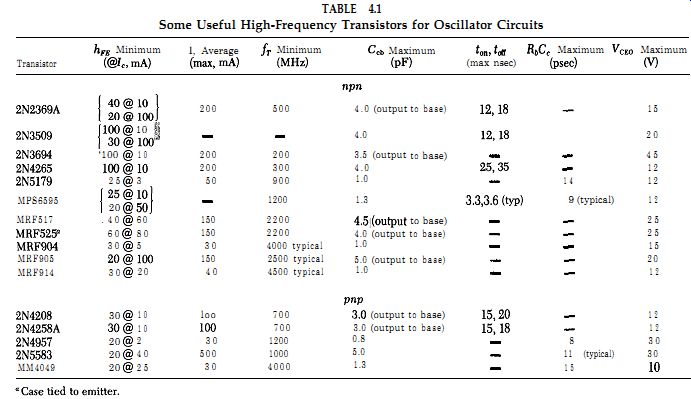
TABLE 4.1 Some Useful High-Frequency Transistors for Oscillator Circuits
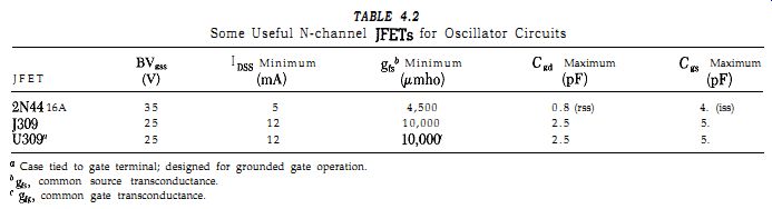
TABLE 4.2 Some Useful N-channel J-FETs for Oscillator Circuits a Case tied
to gate terminal; designed for grounded gate operation.
*&$, common source transconductance.
' pr$, common gate transconductance.
4.6. TRANSISTOR HIGH-FREQUENCY GAIN LIMIT fT
Starting at some frequency in the 1- 100 MHz range, the gain of a bipolar transistor falls off with increasing frequency at approximately 6 dB/ octave, due to the RC roll-off of the intrinsic resistance of the transistor's base material and the base-to-emitter's junction capacitance. On the transistor data sheets, this is specified by the frequency fT, where the transistor's current gain has dropped down to 1, and no amplification can occur. If a transistor has a DC current gain of 100 and f, of 200 MHz, then 2 MHz is the highest frequency at which the full current gain is available. To make an oscillator at 10 MHz, we need a transistor with a f_r of 1000 MHz to get a current gain of 100 at 10 MHz; however, in manufacturers' catalogs, the selection of transistors with f,'s of 1000 MHz or higher is pretty thin. Table 4.1 lists some useful high-frequency transistors for oscillator circuits.
In contrast to the bipolar transistor, the transconductance (or gain) of a FET is constant up to about 1000 MHz. At frequencies of 10-100 MHz, such FET characteristics as high transconductance, minimum input capacitance, and minimum feedback capacitance (Miller effect) are the important ones.
Table 4.2 lists some useful high-frequency FETs for oscillator circuits.