BASIC OSCILLATOR CIRCUITS [Crystal Oscillator Circuits]
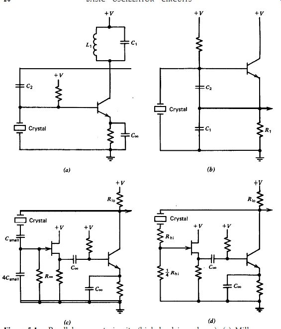
Figure 5.1. Parallel-resonant circuits (high load impedance): (a) Miller-poor
circuit; poor frequency stability. (b) Colpitts-good circuit; fair frequency
stability. Circuit is far more complex than it appears to be; widely used.
(c) Low capacitance load-works reasonably well; fair frequency stability. (d)
High resistance load-works reasonably well; poor frequency stability.
[…] performance. Many of these circuits have a limited frequency range, due
to the wide variation in load and source resistances that a crystal needs to
see over the wide frequency range of 1 kHz-200 MHz.
Figure 5.5 shows two circuits not covered in detail because they have little
to offer. The first is the transformer-coupled circuit in Fig. 5.5.
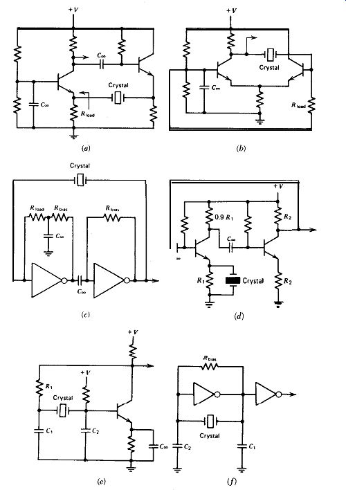
Figure 5.2. Series-resonant circuits (low load impedance): (a) Common base
works very well; good circuit; good frequency stability. (b) Common base, low
frequency-works very well; good circuit. Provides high crystal load resistance
needed at low frequencies; good frequency stability. (c) Two-inverters-IC works
fairly well; fair frequency stability. With TTL, oscillates spuriously when
crystal is removed; widely used. (d) Emitter coupled-works fairly well; good
frequency stability. (e) Pierce-very close to series resonance. One of the
best circuits; very good frequency stability, best overall design; widely used.
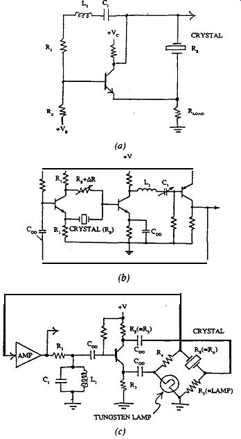
Figure 5.3. Bridge circuits: (a) Feedback bridge, (b) RLC half-bridge, and
(c) Meacham. All operate at series resonance, with L,C1 resonant at oscillation
frequency. All are complex circuits and difficult to design. In-circuit Q is
higher than crystal's internal Q, have best short term stability of any circuit
type.
The transformer provides a 180 degr. phase reversal and allows series-resonant
operation with one transistor instead of two. This had some value in the vacuum
tube era, but today it is more practical to use a second transistor to provide
the 180 degr. phase reversal.
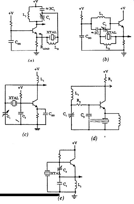
Figure 5.4. Harmonic circuits: (a) Butler common base-operates at or near
series resonance. Fair to poor circuit design. Has parasitics, touchy to tune.
Fair frequency stability. (b) Butler emitter follower-operates at or near series
resonance. Good circuit design. No parasitics, easy to tune. Good frequency
stability. (c) Pierce harmonic-operates 10-40 ppm above series resonance. Good
circuit design. Good to very good frequency-stability. (d) Emitter coupled harmonic
operates at or near series resonance. Circuit somewhat complex. Very good frequency
stability. (e) Colpitts harmonic-operates 30-200 ppm above series resonance.
Physically simple, but analytically complex. Low cost. Fair frequency stability.
The second circuit not covered in detail is the capacitance bridge circuit
in Fig. 5.5b. This circuit cancels out the crystal's terminal shunt capacitance
Co, but the cancellation can be done in a simpler fashion by shunting the crystal
with an inductance and tuning it to parallel resonance
5.2. MILLER
The Miller is a parallel-resonant circuit, and a basic schematic is shown
in Fig. 5.6. The crystal is used as a shunt impedance element to ground.
The voltage across the crystal is amplified and inverted by the transistor
and fed back to the crystal through a small capacitance C2. The collector tank
circuit L,C i is tuned to a frequency above resonance, so that the net impedance
of L,C, is inductive at the frequency of oscillation. The tank circuit L,C,
must be inductive at the frequency of oscillation, or the circuit will not
oscillate. C r is not necessary for the circuit to oscillate, but it cleans
up the waveform across L, considerably, which is absolutely awful without the
capacitor across it.
The circuit operates as follows. The transistor provides a 180 degr. phase
reversal. The tank circuit L,C, is inductive at the oscillation frequency,
and together with the collector's output resistance provides a nominal 90 degr.
phase lead. And C2, together with the crystal operating above resonance as
an inductance, provides 90 degr. more phase lead, so that the total phase shift
around the loop is zero.
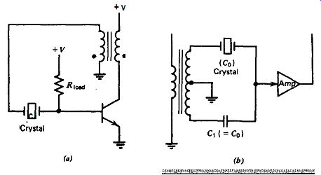
Figure 5.5. Two oscillator circuits not covered in detail: (a). transformer
coupled and (b) capacitance bridge.
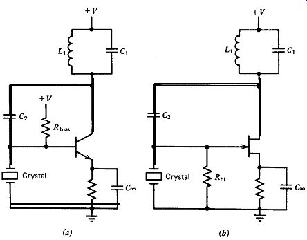
Figure 5.6. Miller circuit: (a) transistor version and (b) FET version.
This is not a good oscillator circuit because the waveforms across the crystal
are very poor and the frequency is unstable. It turns out that the frequency
of oscillation is quite sensitive to the value of the series feed back capacitor
C2, which is about 5-40 pF. Because of the Miller effect, the effective value
of C, consists of the actual capacitor C, shown in Fig. 5.6 plus the transistor's
internal base-to-collector capacitance, both multiplied by the transistor's
voltage gain. The gain changes with temperature, power supply voltage, and
from transistor to transistor. This means that the effective value of C, is
not stable, and as a result, neither is the frequency of oscillation.
The transistor version of the Miller circuit will operate at high or medium
frequencies, but not at low frequencies. At low frequencies, the resistive
loading of the transistor's base input resistance across the high-impedance
crystal is so great that the crystal will not oscillate.
The FET version of the Miller circuit is shown in Fig. 5.6b and can be used
at any frequency: low, medium, or high. The crystal voltage waveform is much
better with a FET than with a transistor. The frequency is still unstable and
for the same reason: variability in the effective feedback capacitance C2 due
to changes in the FET's gain.
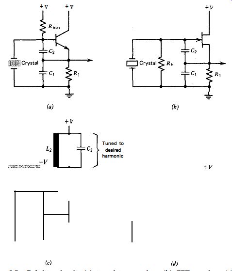
Figure 5.7. Colpitts circuit: (a) transistor version, (b) FET version, (c)
frequency multiplier, and (d) harmonic (L,C, is not tuned to resonance).
5.3. COLPITTS
The Colpitts is a parallel-resonant circuit, and a basic schematic is shown
in Fig. 5.7. Physically, the circuit is very simple, but analytically, it is
very complex. The oscillator has the following three distinct operating states.
The amplifier is an emitter follower with a gain of 1. The transistor conducts
current over only a small portion of each oscillation cycle, usually about
15-20%. The transistor starts conducting a little before (about 10%) its base
reaches the most positive peak of the sinusoid and stops conducting immediately
after the positive peak. At the positive peak, the transistor saturates and
clamps the crystal to the power supply bus through the forward-biased base-collector
junction. Positive peak saturation lasts about 5-10% of an oscillation cycle.
The transistor shuts off and remains nonconducting over the rest (80-85%) of
the cycle. Thus, three circuit conditions exist during each cycle: a short
interval (10%), with the transistor conducting properly and acting as an emitter
follower; a second short interval (5-10%), with the transistor saturated and
shorting out the crystal; and a third long interval (80-85%), with the transistor
shut off and nonconducting.
During the short state when the transistor is on and conducting normally,
the circuit operates as follows. Referring to Fig. 5.7a, the crystal oscillates
in a closed loop in series with C,. C, is in series with the crystal's internal
motional capacitance, which reduces the net capacitance in the crystal loop
and raises the oscillation frequency. At this higher oscillation frequency,
the crystal is inductive, and together with Cf, it generates a phase lead from
the emitter to the base. C1, together with the paralleled sum of R, and the
emitter's output resistance Rout, generates an equal but opposite RC phase
lag, giving zero total phase shift around the amplifier loop from emitter to
base. Voltage gain from the emitter to the base is provided by partial series
resonance between C2 and the crystal's inductance.
During the long state when the transistor is shut off, the voltage across
C, decays at a rate determined by the time constant R,C,. The crystal's in-circuit
Q is sensitive to the time constant R,C,.
What values should be used for Cr, Co, Rr, and R_bias? The answer is that
they should be what the crystal wants them to be, which the crystal indicates
by maximizing the voltage across itself. The biggest factor is external shunt
resistance across the crystal terminals, which is such a strong factor that
it determines the lowest frequency the circuit will oscillate at. This shunt
resistance is the parallel sum of the biasing resistor Rb1,, and the transistor's
input resistance. The transistor's input resistance is determined by the transistor's
gain and the emitter's load resistance R 1. Using a high-gain transistor for
the emitter follower helps considerably in raising shunt resistance across
the crystal.
Not too surprisingly, there is a minimum crystal shunt resistance below which
the crystal will not oscillate. This minimum shunt resistance value varies
directly with the crystal's internal series resistance R,, which varies inversely
with frequency. Table 5.1 lists two shunt-resistance values as a function of
frequency: One is the shunt resistance at which the crystal's voltage amplitude
drops lo%, and the other is the shunt-resistance value below which the circuit
will not oscillate. These data were taken from several test circuits, so they
are typical rather than exact.
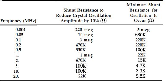
TABLE 5.1 Minimum Crystal Shunt Resistance in Colpitts Circuit
As to the other component values in the Colpitb circuit, some change with
frequency and some do not. In a transistor circuit, C, should be a fixed value
of 40-70 pF, independent of oscillation frequency. The oscillation frequency
is very sensitive to the value of C2, but not to C,. The time constant R,C,
should vary inversely with the oscillation frequency; that is, where R, is
in ohms, C, is in pF, and f is in MHz. Additionally, there is no requirement
for any specific ratio of C, to C,.
Now, since the crystal's shunt resistance has to increase as the frequency
drops, two requirements can be met at the same time in the transistor circuit
by holding C, fixed and varying R1 inversely with frequency. Increasing R,
really helps raise the crystal's shunt resistance, because, in addition to
increasing the input resistance of the emitter follower, it also raises the
value of the biasing resistor R_bias. This technique of varying R I and holding
C 1 fixed works very well in practice. The graph in Fig. 5.8 shows some typical
values for R, and C, in the transistor Colpitts circuit as a function of frequency.
R, and C, values for Colpitts-transistor circuit.
The Colpitts circuit works better with a FET than a transistor. Figure 5.7b
is a schematic of a Colpitts circuit using a FET. The main advantages are:
(1) a better crystal waveform; (2) minimum oscillation frequency is lowered
from 200 kHz (transistor) to 1 kHz (FET); (3) a higher crystal shunt resistance,
which gives a higher in-circuit Q; and (4) no parasitic effects. The drawback
to the FET is that above 10 MHz it does not work as well as the transistor
circuit. This is because the output resistance of a FET source follower, which
is 10 times higher than that of a transistor emitter follower, has a hard time
driving the low load impedance that exists in the circuit at 10 MHz and above.
With a FET, the waveform across the crystal is less distorted and more of a
sine wave, as the waveform in Fig. 10.3a shows.
The minimum Colpitts oscillation frequency is lower with a FET than with a
transistor, because the crystal's shunt-load resistance can be made higher
with the FET. Table 5.1, for example, shows that at 4 kHz, a crystal shunt
resistance of 220 MR will reduce voltage amplitude across the crystal by 10%
and a shunt resistance lower than 5 MS1 will prevent oscillation. These are
not practical values with a transistor circuit, but they are with a FET circuit.
In the FET version of the Colpitts oscillator shown in Fig. 5.7b, the value
of the crystal's shunt resistance &,i is picked from Table 5.1 as the value
that will not decrease oscillation amplitude by more than 10%. C2 should be
a fixed value of 22-33 pF, independent of oscillation frequency (in the transistor
circuit, C2 should be a fixed value of 40-70 pF).
The oscillation frequency is very sensitive to the value of C2, but not to
C,. And like the transistor circuit, the time constant R,C, varies inversely
, with frequency:
where R1 is in ohms, C1 is in pF, and f is in MHz.
To meet the inverse frequency requirement on the time constant R,C, in the
FET-Colpitts circuit, it is convenient to hold RI constant at some convenient
biasing value and vary C, with the frequency of oscillation.
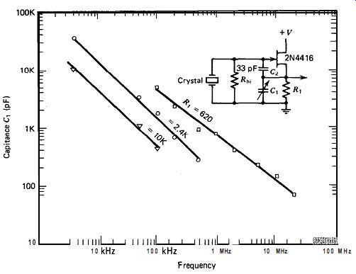
Figure 5.9. R1 and C, values for Colpitts-FET circuit.
This is in contrast to the transistor-Colpitts circuit, where it was convenient
to hold C, fixed and vary RI. The graph in Fig. 5.9 shows some typical values
of R, and C, as a function of frequency for the FET Colpitts circuit. Additionally,
there is no requirement for any specific ratio of C, to C,.
In the transistor-Colpitts circuit, parasitics will occur at some non-optimum
circuit values. In contrast, no parasitics of any kind have been found in the
FET-Colpitts circuit. The parasitics turn out to be third harmonic oscillations
or a combination of fundamental and third harmonic oscillations. The circuit
values are rather critical for obtaining this harmonic oscillation. The effect
can be enhanced by decreasing the crystal's shunt resistance down to a point
where the fundamental frequency is discouraged from oscillating while still
keeping the shunt resistance high enough to permit oscillation at the third
harmonic. Setting the time constant R,C, for the third harmonic frequency also
helps. Both third and fifth harmonic oscillation have been reported by Bahadur
and Parshad [16]. The amplitude of oscillation obtained this way is rather
low, and there is a better harmonic Colpitts circuit available, which is discussed
in the following paragraphs.
The Colpitts can also be used as a harmonic multiplier and a harmonic oscillator,
as shown in Figs. 5.7 and 5.7d. In Fig. 5.7c, an LC tank tuned to the desired
harmonic is placed in the collector circuit, where it is isolated and has very
little effect on what happens to the crystal at the transistor base. The crystal
runs at its fundamental frequency, and the collector's L,C3 tank at a harmonic.
The transistor conducts during only a short interval in each cycle (about S-15%
of the cycle period) at the crystal's fundamental frequency, which gives a
short, sharp pulse of excitation once per fundamental cycle to the harmonically
tuned tank in the collector circuit. The harmonic tank rings at its own natural
frequency and is essentially resynchronized to the crystal's fundamental frequency
once per fundamental cycle. This circuit has two drawbacks:
The frequency is not constant from cycle to cycle, and the amplitude varies
over the resynchronization interval.
In Fig. 5.7d, the crystal itself oscillates at the harmonic frequency.
This circuit works much better than the circuit in Fig. 5.7. Figure 5.7d shows
a FET amplifier, but the circuit works equally well with a transistor. The
only difference between this harmonic circuit and the fundamental circuit in
Fig. 5.7b is that the resistor R, is replaced with the inductor L1. The key
to harmonic operation is to select L, so that its impedance at the harmonic
oscillation frequency is equal to what R, in Fig. 5.7b should be to oscillate
at that same frequency.
As an example, Fig. 5.10 shows a fundamental Colpitts circuit for 20 MHz.
Figure 5.11 shows a third harmonic Colpitts circuit also for 20 MHz. Note that
the impedance of the 10 /.LH inductor& is approximately equal to RI, 1200
ohm . The reason the circuit in Fig. 5.11 oscillates at the third harmonic
(20 MHz) rather than at the fundamental (6.7 MHz) is that the impedance of& should
be 3600 0 at 6.7 MHz for fundamental oscillation to occur, whereas the actual
impedance of L, at 6.7 MHz is only 400 R or l/s of what it should be for fundamental
oscillation.
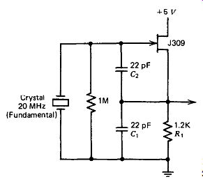
Figure 5.10. Fundamental Colpitts at 20 MHz.
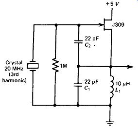
Figure 5.11. Third harmonic Colpitts at 20 MHz.
5.4. LOW CAPACITANCE LOAD
What happens when a low capacitance load (high impedance) is used on the crystal?
The major effects are a higher oscillation frequency and a higher crystal output
signal to the amplifier. The external load capacitance is in series with the
crystal's internal motional capacitance, which reduces net oscillation capacitance
and raises the resonant frequency proportionately. The output signal is larger
because the impedance of the crystal's current measuring element is larger.
A basic schematic is shown in Fig. 5.12. The crystal is driven by as low a
source resistance as possible R1,. The crystal's load consists of two small
capacitors in series that act as a 5 to 1 voltage divider to isolate the amplifier's
resistive loading and overload peak-clipping effects from the crystal. The
amplifier's input stage is a FET in order to make the amplifier's input resistance
as high as possible and minimize resistive loading effects on the crystal.
The 5 to 1 capacitive voltage divider and, to a certain extent, using a FET
input stage provide a linear input impedance to the crystal that will not overload
and put a short circuit directly across the crystal over a part of the waveform
cycle, as the Colpitts circuit does. The FET does over load as a gate-to-drain
diode clamp to the power supply bus at the positive peak of the input waveform,
but the 5 to 1 voltage divider hides it from the crystal.
Sampling the crystal current by means of the voltage across a capacitor in
series with the crystal introduces a 90 degr. phase lag in the amplifier loop.
The amplifier itself provides a 180 degr. phase inversion, and the two RC
networks (R,CB and R&J in the amplifier introduce two additional 45 phase
lags, for a total phase shift of 360 degr. around the amplifier loop.
Figure 5.12. Low capacitance load circuit: (a) using an inverting amplifier,
(b) using a noninverting amplifier.
The oscillator works equally well with a noninverting amplifier, as shown
in Fig. 5.12b. The noninverting amplifier consists of a cascaded FET source
follower and a transistor emitter follower, with a total amplifier gain of
0.7X. Additional gain is obtained by resonance effects between the inductive
crystal and the series capacitors C_small and 4C_small, and between 15, and
C,. The 90 degr. phase lag of the crystal's current sampling capacitor 4C_small
is compensated by the 90 degr. phase lead of L1, which is series resonant with
C,. The overall loop gain is controlled by two ratios: the ratio of the impedance
of L1 to R1 and the ratio of the impedance of 4C,rr to the impedance of L1.
L, is made relatively small and partially reduces the frequency increase caused
by the low capacitance load C_small on the crystal.
5.5. HIGH RESISTANCE LOAD
What happens when a high resistance load is used on a crystal? Pretty much
the same thing that happens when a low capacitance load is used.
The major effects are a much higher oscillation frequency and a larger crystal
output voltage to the amplifier. The higher oscillation frequency is due to
the crystal's small terminal capacitance Co being in series with the crystal's
internal-motional capacitance, which reduces net oscillation capacitance and
raises the resonant frequency.
A basic schematic is shown in Fig. 5.13. The circuit is very similar to the
low capacitance load circuit in Fig. 5.12 except for the crystal loading.
The crystal is driven by as low a resistance as possible, R1,. The crystal's
load consists of its terminal capacitance Co and two very large resistors (R_hi
and 0.25 R_hi) that act as a 5 to 1 voltage divider to isolate the amplifier's
overload peak-clipping effects from the crystal. The amplifier's input stage
is a FET in order to make the amplifier's input resistance as high as possible
and minimize crystal loading. The 5 to 1 voltage divider provides a linear
impedance to the crystal that will not put a short circuit across the crystal
over a part of the waveform cycle, as the Colpitts circuit does. The FET overloads
as a gate-to-drain diode clamp at the positive peak of the input waveform,
but the 5 to 1 voltage divider hides it from the crystal.
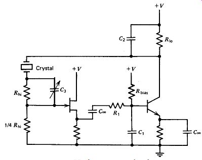
Figure 5.13. High resistance load circuit.
The input capacitance of the FET amplifier in Fig. 5.13 is 4 pF, which requires
capacitive compensation C3 of the resistive voltage divider. The reactive impedances
of C, and the amplifier's 4-pF input capacitance at 1 MHz are much lower than
the resistance of the voltage divider, which means that the divider is really
a capacitive divider rather than a resistive one, It also means a 90 degr.
phase lag, because the crystal's current is measured by the voltage drop across
;t capacitor rather than across a resistor.
The amplifier in Fig. 5.13 provides 180 degr. phase inversion. The two RC
networks (R,C, and R&,) introduce two additional 45 degr. phase lags, for
a total phase shift of 360 degr. around the amplifier loop. The oscillator
will work equally well with a noninverting amplifier, using a circuit similar
to that shown in Fig. 5.12h but with a high-resistance voltage divider instead
of the capacitive one shown in Fig. 5.12b.
5.6. COMMON BASE
The common base oscillator circuit is a series-resonant type, and a basic
schematic is shown in Fig. 5.14. This circuit has several good design characteristics:
It uses a common base amplifier, which is un-condition ally stable at all frequencies
and has a very wide frequency response. An emitter follower reduces the amplifier's
output resistance to a low value for driving the crystal. The crystal is tied
between two emitters; one emitter acts as the crystal's load resistance and
the other, as the crystal's source resistance. The emitter source and load
resistances can be varied over a wide range to provide a suitable crystal load
over a wide range of crystal resistances.
The basic circuit works well over a frequency range of 600 kHz-20 MHz. The
frequency range can' be extended to 4 kHz by moving the crystal to a different
part of the circuit, as shown in Fig. 5.14.
The common base circuit shows very clearly the strong effect that the crystal's
internal series resistance R, has on circuit design. Referring to Fig. 5.14a,
we see that the net load resistance on the crystal is the parallel sum of R_1
and Q_1's emitter input resistance. The net load resistance and the crystal's
internal series resistance R, act as a voltage divider, which reduces loop
gain. The lower the load resistance on the crystal, the more loop gain is reduced,
and the larger the gain that Q1 has to provide to maintain oscillation.
The gain of Q, is proportional to the ratio of its collector and emitter resistors
R,IR2. So to keep the gain up, the emitter resistor R2 should be kept small,
and not allowed to get much bigger than Q1's emitter input resistance. The
emitter's input resistance is controlled by the emitter current, which can
be varied over a wide range by varying the base bias voltage.
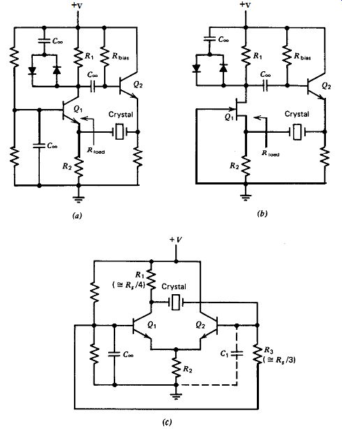
Figure 5.14. Common base and common gate oscillator circuits. The appropriate
circuit is selected on the basis of the crystal's internal series resistance
R,. (a) At high frequencies: 5 < R, < 400 a; (b) At medium frequencies:
200 < R, < 1200 R; (c) At low frequencies: 1K < R, < 100K a.
A transistor emitter's input resistance can be varied from 5 to 100 ohm, which
is suited to the low resistance of crystals at high frequencies. At medium
frequencies, replacing the transistor Q1 with a FET will give the crystal a
higher load resistance that is more appropriate to the medium resistance of
crystals at these frequencies.
Figure 5.14b shows a FET schematic that is appropriate for medium frequency
use. The source input resistance for a high transconductance FET such as the
5309 (or U309) is about 200 ohm and for a medium transconductance FET such
as the 2N4416, about 500 ohm. The crystal's load resistance can thus be varied
from 200 to 500 ohm by selecting the FET used for Qr.
It is important to note the diode amplitude clamp in Figs. 5.14~ and 5.14b;
the circuits do not work well without it. The purpose of the clamp is to limit
oscillation amplitude and thereby keep both Q1 and Q2 operating in their linear
regions over the complete waveform cycle. If either transistor saturates or
ceases conduction at some point over the waveform cycle, the crystal's source
and/or load resistances will switch suddenly to either a short circuit or a
high value.
At low frequencies (i.e., below 600 kHz), crystals have a relatively high
internal series resistance and need a high load resistance to avoid a large
gain loss. To obtain this, the crystal is moved to a higher impedance part
of the circuit, as shown in Fig. 5.14. Here, the crystal is tied between collector
and base. The two emitters are tied together and use a common emitter resistor.
Q2 should be a high-gain transistor in order to maximize both its base input
resistance and the biasing resistor R3 in parallel with the base of Q2. Q2
acts as an emitter follower driving Q1 as a common base amplifier. The gain
of Q1 is controlled by the ratio of the collector and emitter resistors R1/R2.
C, i's a small noise-reducing capacitor, which eliminates extra noise switchings
that occur at switching crossover points at these low frequencies.
At very low frequencies (below 4 kHz), where the crystal's internal series
resistance R, goes over 100K-ohm, the circuit in Fig, 5.14 does not have enough
gain to oscillate anymore because of the high gain loss through the crystal
and its voltage divider. The circuit in Fig. 5.15 can then be used; it is not
a common base amplifier circuit, but it is a series resonant circuit. It uses
a straightforward two-stage amplifier, with a FET for the input stage. There
is more than enough gain available, so the crystal's source and load resistances
R, and R_Load can both be made considerably smaller than the crystal's internal
series resistance R,. This will give good in-circuit Q and good short-term
frequency stability.
5.7. SERIES RESONANCE-IC
There are several ways integrated circuits can be used in a crystal oscillator.
The two-inverter circuit shown in Fig. 5.16 is a popular one be cause of its
simplicity and the ease of blending it into digital circuitry.
The circuit is series resonant and uses two cascaded digital inverters for
an amplifier. It can be built using CMOS-, TTL-, or ECL-type circuitry.
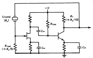
Figure 5.15. Alternative series-resonant circuit at very low frequencies,
for R, > 50K ohm.
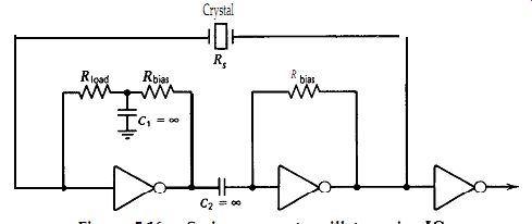
Figure 5.16. Series-resonant oscillator using ICs.
To solve the start-up problem, each inverter has a DC biasing resistor tied
from its output to its input to bias the inverters halfway between the zero
and one states, so that they will amplify when power is applied and the crystal
will start oscillating. The two inverters are AC coupled to prevent the DC
biasing loops on the two inverters from interfering with each other.
The biasing resistor on the first inverter is made up of two resistors in
series, with the center point bypassed to ground through Cr. C, reduces the
coupling of the switching signal from the output of the first inverter back
into the crystal's output and helps clean up the crystal's output waveform.
For good in-circuit Q and short-term frequency stability, R_load should be
set equal to or somewhat less than the crystal's internal series resistance
R,.
The two-inverter circuit works well in CMOS and ECL, but in TTL, it has three
drawbacks. First, the input resistance of a TTL inverter (or gate) goes low
just before the instant of switching, creating a flat spot in the amplifier's
input waveform at the worst possible time-during the switching interval. The
flat spot makes the instant of switching more un certain in time and worsens
the oscillator's short-term stability. Second, the TTL version cannot be used
above about 3 MHz because TTL voltage levels exceed the crystal's power dissipation
limit. And third, the circuit will not oscillate below about 100 kHz because
the parallel resistance of the first TTL inverter's input resistance and the
biasing resistor R_bias act as a voltage divider with the crystal's internal
series resistance R, and attenuate loop gain too much.
Although Fig. 5.16 shows a crystal load resistor Rload, both R_load and capacitor
C r are frequently omitted from the circuit, which reduces both the in-circuit
Q and short-term frequency stability. Many computer circuits simply need a
reliable clock with a 50-50 on/off ratio rather than the accuracy or stability
provided by a quartz crystal. Therefore, omitting R_load and C, is not a loss
under these conditions.
Another IC oscillator circuit is shown in Fig. 5.17. This is a series resonant
circuit that uses a voltage comparator or a line receiver for the amplifier.
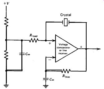
Figure 5.17. Another series-resonant IC oscillator.
-----------
5.8. PIERCE
The Pierce is a series-resonant circuit, and its schematic is shown in Fig.
5.18. The Pierce has many desirable characteristics. It will work at any frequency
from the lowest to the highest-from 1 kHz-200 MHz. It has […] circuits. One
set of equations can be applied to both circuits, but since the two circuits
operate differently, the equations must be interpreted differently in the two
cases. The basic difference between the circuits is that the crystal in the
Pierce is designed to look into the lowest possible impedance across its terminals,
whereas the crystal in the Colpitts is de signed to look into a high impedance
across its terminals. This basic difference results in other differences. The
operation of the Colpitts, which is described in Section 5.3, is so different
from that of the Pierce, de scribed in this section, that there is little significance
in using the same set of equations to cover both circuits except that both
are three-loop networks containing the same number of RLC components.
To understand how the Pierce oscillator circuit works, the reader should refer
to Fig. 5.18. The total phase shift around the loop is 360 degr.
Idealistically speaking, the amplifier provides 180 degr., R,C 1 acts as an
integration network and provides a 90 degr. phase lag, and the crystal, together
with C2, acts as a second integration network and provides a second 90 degr.
phase lag.
At series resonance, the crystal's impedance is a pure resistance, and together
with C2, it acts like a RC integrating network, providing a 90 degr. phase
lag, as shown in Fig. 5.18. Below series resonance, the crystal's impedance
is capacitive, as shown in Fig. 5.18, and together with C2, it acts like a
capacitive voltage divider with 0 degr. phase shift. Above series resonance,
the crystal's impedance is inductive, as shown in Fig. 5.18, and together with
Ct, it provides a 180 degr. phase lag. Thus, the crystal can provide anything
from a 0 degr. to 180 degr. phase lag by just a small increase or decrease
in frequency from series resonance.
In reality, of course, the amplifier provides slightly more than a 180 degr.
phase shift, due to the transistor's internal capacitance and storage time,
and the R,C, integrating network provides something less than a 90 degr. phase
shift. Figure 5.19 shows more practical phase-shift values to be expected in
a Pierce circuit. The crystal typically operates inductively, about 5-40 ppm
above series resonance, because the actual phase lag of R,C, is significantly
less than 90 degr.
There is a close correlation in the Pierce between the circuit's short-term
frequency stability and the crystal's internal series resistance R,.
The lower the crystal's resistance at series resonance, the smaller the frequency
shift needed to change the crystal's impedance from capacitive to inductive
(or vice versa) and correct any phase errors around the loop.
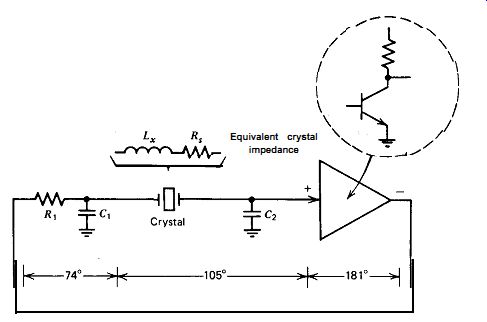
Figure 5.19. Pierce circuit, actual operation (slightly above series resonance).It
was mentioned earlier that the oscillator's frequency is relatively insensitive
to small changes in resistance and capacitance values. The reason is that the
phase lag of each RC integrating network (R,C, and R,C,) is much greater than
45 degr., and a small change in either the resistance or capacitance of such
a network introduces only a very small change in its phase lag. Changes in
either R or C will introduce significant gain changes, of course, but only
small changes in phase.
To design a Pierce oscillator, the frequency of oscillation and the crystal's
internal series resistance R, must be known. The crystal's internal series
resistance need be known only approximately. This can be obtained by referring
to Fig. 2.3, which gives the maximum series resistance of crystals at various
frequencies. The typical crystal's internal series resistance is about % of
the maximum value given in Fig. 2.3. The time constants of the two RC phase-shifting
networks should be made as large as possible. This makes their phase shifts
as independent as possible of any changes in resistance or capacitance values.
Such networks have large gain losses, which mean that the transistor used for
the amplifier should be selected on the basis of having the highest possible
gain in order to compensate for these losses.
The highest gain RF transistors have a minimum current gain hFE of 100. This
allows a maximum amplifier voltage gain of about 50. To maintain oscillation,
we need a net loop gain of 1.5-2, which gives a gain of about 50/1.7 = 30'
to cover the losses of the two RC networks. Dividing this gain of 30 equally
between them allows each to have a gain loss of about 5.5. This defines the
capacitive shunt reactance in each RC net work as 1/5.5 or 0.18 its series-resistance
value. Thus, the shunt capacitance C2 on the crystal's output should have a
reactance of 0.18 the crystal's series resistance. With the known frequency
of oscillation, the actual capacitance value can be calculated.
To minimize loading effects of the crystal's internal series resistance R,
on C1, the reactance of C, should be much lower than the series resistance
of the crystal, say 1/5 of it, which means that C, should be approximately
equal to Cp. This also means that R1 should be approximately equal to the crystal's
internal series resistance R8. R1 frequently turns out to be a little low for
the transistor to drive conveniently, so it is often fudged upward a little
to a value that the transistor can drive more easily, and the impedance of
C, is fudged upward along with it to avoid any additional gain loss.
The preceding describes a typical Pierce circuit at middle frequencies. At
low frequencies, the amplifier's input stage' must be a FET to avoid resistive
loading of the crystal's high internal series resistance R, at low frequencies.
And at high frequencies, the amplifier's output stage must be an emitter follower
in order to be able to drive the low impedance of the crystal at high frequencies.
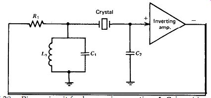
Figure 5.20. Pierce circuit for harmonic operation. L,C, is not tuned to the
harmonic oscillation frequency.
For harmonic operation, either of two approaches can be used. With the first
approach, a resonant LC tank tuned to the desired harmonic is incorporated
somewhere within the amplifier. The second approach uses the circuit shown
in Fig. 5.20.
The circuit in Fig. 5.20 is the same as the one in Fig. 5.18 except that an
inductor L1 has been added in parallel with C1. L1 is picked to parallel resonate
with C, at some intermediate frequency (say halfway) between desired harmonic
oscillation frequency and the next lower odd harmonic. At the desired harmonic
frequency, the impedance of L, will then be high enough with respect to the
impedance of C, so that it can be neglected, and R,C, will act as an integrating
network and provide the desired 90 degr. (idealistically speaking) phase lag.
Thus, the circuit will oscillate normally at the desired harmonic. At all lower
harmonics, however, the impedance of L1 will be lower than the impedance of
C r. Then, C, will be negligible instead of LX, and R1L1 will act as a differentiating
network, providing 90 degr. of phase lead instead of phase lag. The circuit
will not oscillate at any of these lower harmonics because the total phase
shift around the loop at these lower frequencies is now 180 degr., which provides negative feedback and stabilizes the circuit instead of making it oscillate.
The shunt inductance scheme in Fig. 5.20 is useful at medium and high frequencies,
but it is redundant at VHF. Above 20 MHz, the amplifier has to use a tuned
LC tank as a load to get any gain at all, and this same LC tank can be used
to select the desired harmonic without adding an extra inductor in front of
the crystal.
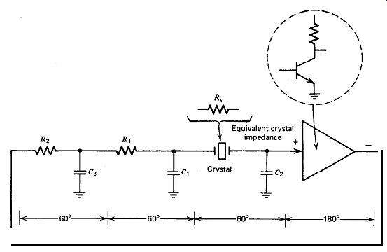
Figure 5.21. Pierce at exact series resonance.
The Pierce can be made to oscillate exactly at series resonance rather than
just slightly above it by using the circuit in Fig. 5.21. The technique is
to use three RC lag networks, each providing a 60 degr. phase lag. In each
RC lag network, capacitance C is determined by setting its capacitive reactance
equal to 0.5R in order to give the 60 degr. phase lag required. Nominally,
R, = R, = R,, and C, = C, = C,. Because of loading effects of each RC network
on the preceding one, capacitance values of C, and C3 will have to be shifted
a little to provide the 60 degr. phase lag needed in each RC network. The quickest
way to do this is by experiment, trimming the values of C, and C, to get the
desired 60 degr. phase lag in each network. A scope is used to measure the
actual phase shifts obtained. Capacitance values can also be determined by
mathematical circuit analysis.
The Pierce circuit in Fig. 5.21 can be made to oscillate below series resonance
as well as exactly at resonance. The only change required is increasing the
phase lags of R2 C3 and R1 C1i to a little more than 60 degr., The circuit
in Fig. 5.21 requires less amplifier gain than other Pierce circuits, which
is helpful if the amplifier to be used is a little short of gain. Each 60 degr.
RC phase-lag network has a gain loss of 0.5X, and an amplifier gain of 16 will
provide a net loop gain of two, which is sufficient for proper oscillation.
5.9. PIERCE-K
This section covers implementing the Pierce oscillator with integrated circuits,
but does not discuss how the Pierce circuit works, which is treated in Section
5.8.
The Pierce amplifier can be built using digital logic elements in CMOS, TTL,
and ECL. The basic frequency range of each technology applies to crystal oscillators;
that is, CMOS for low frequencies, TTL for medium frequencies, and ECL for
medium and high frequencies. Two primary considerations in each technology
are (1) obtaining the high amplifier gain required by the Pierce circuit and
(2) the amount of internal phase shift or time delay in the amplifier (or inverter).
Each technology will be discussed in turn.
In CMOS, both the gain and frequency bandwidth of a single inverter stage
vary widely from manufacturer to manufacturer. The A series are unusable for
oscillator purposes because of their low inverter gains of 1.1-2 and their
lack of output drive power. B series inverters have gains of 10-30. The widest
bandwidth (i.e., the least delay) CMOS inverter tested was manufactured by
Solid State Scientific, followed by National Semiconductor's 74C series.
A single CMOS inverter is frequently used as the amplifier in the Pierce circuit
in Fig. 5.22. The gain of a CMOS inverter is too low to use the normal Pierce
circuit in Fig. 5.19, so the resistor R, is eliminated and replaced with the
internal output resistance R, of the CMOS inverter, as shown in Fig. 5.22.
This reduces gain loss and allows operation with a single CMOS inverter. The
inverter's output voltage swings between zero and one are then highly sloped,
and amplitude is sometimes below normal. A second CMOS inverter is added as
an external isolation amplifier in order to square up the output signal and
ensure getting a full rail-to-rail voltage swing.
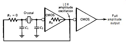
Figure 5.22. Pierce in CMOS. R_1 is replaced by the inverter's output resistance
R_0.
Using the CMOS inverter's output resistance to replace R, in Fig. 519 has
the disadvantage that the crystal is driven at a much higher voltage level
than it would be in a normal Pierce circuit. At frequencies above 2 MHz, the
crystal's power dissipation should be checked to make sure it is within the
maximum dissipation limit.
In TTL, only a voltage comparator IC can be used to make a Pierce oscillator.
Ordinary TTL inverters have gains of only 3-9X, which is not enough to make
a Pierce out of a single inverter. Cascading three inverters in series to increase
gain will not work either, because very bad parasitic oscillations occur during
the switching interval when a TTL inverter's output voltage moves less than
a full voltage swing. TTL line receivers will not work because their gain of
about 15X is too low. In order to make a TTL oscillator using something other
than a voltage comparator IC, it is necessary to use the series-resonant two-inverter
type circuit, which is described in Section 5.7.
In ECL, a single line receiver does not have enough gain to make a Pierce
oscillator. But three I0114 line receivers can be cascaded in series to get
enough gain. A single 10114 receiver has a gain of 3-6X. The 10116 and 10216
are apparently constructed differently than the 10114, since the units tested
showed wider gain variations than the 10114 and exhibited relatively large
gain differences between a receiver's two outputs (normal and inverted).
Although a relatively high gain may be desirable in an IC for oscillator circuitry,
it should be said that a high gain per stage is undesirable in digital circuitry,
which is what many of these ICs are designed for. High gain increases the tendency
for spurious oscillations (caused by stray feedback) during the digital switching
interval. A low stage gain of 1.5-3X is sufficient in a digital IC, since the
primary purpose of gain in a digital IC is to prevent a low amplitude signal
from propagating throughout the system.
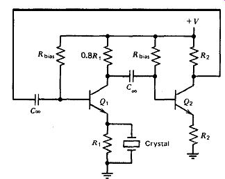
Figure 5.23. Emitter coupled oscillator.
5.10. EMITTER COUPLED
The emitter coupled oscillator is a series-resonant circuit, and a basic schematic
is shown in Fig. 5.23. The oscillator has a positive feedback amplifier with
a loop gain of slightly less than one without the crystal, so that the circuit
will not oscillate by itself. Loop gain is controlled by the ratio of the collector
to emitter resistances in each transistor stage. In the second stage, it is
convenient to make emitter and collector resistances (R2 and R2) equal to each
other, giving a stage gain of 1X. The second stage inverts the signal and provides
positive feedback.
In the first stage, the collector resistor 0.8R, is made a little smaller
than the emitter resistor R1 in order to give an overall loop gain of 0.8X.
The value of the emitter resistor R1 is set equal to about twice the crystal's
internal series resistance R,. When the crystal is tied in parallel with R,,
the effective resistance of the emitter resistor is reduced at series resonance,
since the crystal's internal resistance R, is in parallel with R1.
This raises both stage gain and overall loop gain to about 2X, and the circuit
oscillates at the crystal's series-resonant frequency.
An advantage of this circuit is that the crystal sees a very low resistance
load. This low resistance load consists mostly of the emitter's input resistance,
which is much lower than RI. A disadvantage is that circuit waveforms vary
with the circuit's stray capacitance, because loop gain is almost high enough
to oscillate at any frequency.
5.11. MODIFIED MEACHAM
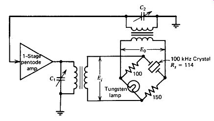
Figure 5.24. Meacham resistance bridge.
The Meacham is a resistance-bridge circuit, as shown in Fig. 5.24.
The crystal is located in one arm of the bridge. A tungsten lamp, located
in another arm of the bridge, is used as a variable resistance-amplitude control.
There is no voltage out of the bridge at exact bridge balance, so it operates
slightly off-balance-just enough to get a loop gain of exactly 1X around the
amplifier circuit. The tungsten lamp's resistance increases with the applied
voltage, and its variable resistance automatically controls loop gain at exactly
1X. This provides a constant sine wave excitation voltage to the crystal. The
amplifier has a large voltage gain Et/E, of 422X.
Clapp's version of the Meacham is shown in Fig. 5.25. The ad vantage
of Clapp's arrangement is the elimination of transformers by using a split-load
phase inverter to drive the bridge. Vacuum tube Vz in Fig. 5.25 has equal cathode
and plate voltages of opposite phase for
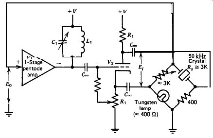
Figure 5.25. Clapp's version of the Meacham resistance bridge. Note that it
has no transformers.
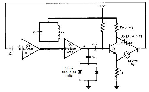
Figure 5.26. Modified Meacham half-bridge.
driving the bridge. Clapp's amplifier also has a large voltage gain EJE, of
about 300X. Both of these circuits use a single stage of amplification, a pentode
vacuum tube.
If something other than a tungsten filament is used for amplitude control,
the Meacham can be simplified further into the half-bridge arrangement shown
in Fig. 5.26, which uses a diode clamp for amplitude control. A thermistor
(which has a negative temperature coefficient of resistance) can also be used
for amplitude control by putting it in the half-bridge in place of Es. Oscillation
amplitude must be at least four times greater if a thermistor is used rather
than a diode clamp, since the thermistor requires a minimum of 4-6 Vp-p to
properly activate its negative resistance characteristic. Greater oscillation
amplitude increases power dissipation in the crystal, which is undesirable.
The advantage of the Meacham is its extremely good short-term frequency stability.
This can be seen by looking at Fig. 5.26 and treating the output of the half-bridge
at point A as a summing point for two input signals. At series resonance, the
amplitude of the positive signal from the emitter of Qs is limited at A by
the crystal's internal series resistance R,.
At the same time, the amplitude of the negative signal from the collector
of Q3 is limited at point A by R3, which if set equal to R,, will cancel out
the positive resistive signal from the emitter. What is happening is that the
crystal's internal series resistance (but not its internal inductance or capacitance)
is being canceled out by the reverse-phase signal through R3. The crystal's
in-circuit Q increases, and its effective internal resistance decreases. In
theory, with exact cancellation of the crystal's internal resistance by RB,
the crystal's Q would approach infinity. In practice, this cannot happen, since
R3 must be slightly larger than R, to get some signal gain (greater than zero)
through the bridge. With high amplifier gain, less gain is required through
the bridge to maintain oscillation, and R3 can cancel out a larger percentage
of the crystal's internal resistance.
Thus, there is a strong advantage in using the highest possible amplifier
gain, since that will give the highest possible cancellation of the crystal's
resistance and the highest in-circuit Q.
The disadvantage of the Meacham is that it has a strong tendency to oscillate
parasitically at high frequencies. It is very difficult to design a stable
Meacham circuit. The cause of this can be seen in the bridge's gain versus
frequency transfer function, as shown in Fig. 5.27. Figure 5.27 shows that
the gain at the crystal's resonant frequency is much less than 1X and 1X at
all other frequencies. To oscillate, the circuit has to have enough amplifier
gain to bring the low bridge gain at resonance up to a net loop gain of at
least 1 or 2X, which means that the gain at all other frequencies is undesirably
much higher than this. To prevent parasitic oscillation, this high loop gain
at frequencies away from resonance must be reduced to less than 1X while introducing
less than 180 degr. additional phase shift. To do this involves consideration
of Bode's stability criteria for feedback-type amplifiers, which is too broad
a subject to cover here.
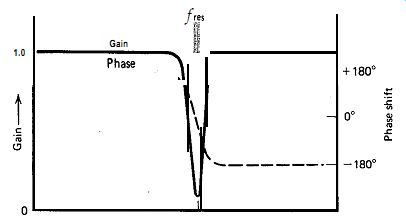
Figure 5.27. Resistance bridge gain and phase versus frequency for the normal
operating condition R3 > R5.
Figure 5.24 shows that Meacham used two resonant LC tank circuits to roll
off loop gain at frequencies away from resonance. Figure 5.25 shows that Clapp,
with a lower loop gain, used only one resonant LC tank circuit to reduce the
gain at frequencies away from resonance. The f res Gain 1.0 modified Meacham
half-bridge circuit in Fig. 5.26 uses one resonant LC tank to roll off loop
gain at frequencies away from resonance.
The modified Meacham half-bridge circuit has two additional characteristics
of interest. The first is that the sequence of placing the resonant LC tank
before the diode amplitude clamp in Fig. 5.26 is significant, since this provides
a square wave drive to the crystal. Reversing the sequence will provide a sine
wave drive to the crystal. The second characteristic of interest is that the
two output signals from the split-load phase inverter Q3 in Fig. 5.26 do not
have to be of equal amplitude.
Necessary bridge balance is maintained by adjusting the ratio of R3 to the
crystal's internal series resistance R, in proportion to the amplitude ratio
of Qa's emitter and collector signals.
It turns out to be very helpful to reduce the collector's output signal from
Q3 in Fig. 5.26 by a factor of two or more with respect to that from Q3's emitter.
This is done by reducing the value of R2 to one-half (or one-fourth or one-eighth)
of R,. Doing this has three advantages. First, R3 is reduced proportionately
with R2 to maintain bridge balance. This lowers the crystal's load resistance,
which consists mostly of Ra, and improves short-term frequency stability. Second,
all frequencies away from resonance pass through R, and the collector of Q3
rather than through the crystal. Reducing R2 with respect to R, reduces loop
gain at all frequencies away from resonance without affecting loop gain at
resonance. This helps the high-frequency parasitic oscillation problem considerably.
And third, R1 feeds back to the base of Q3 a larger percentage of the collector's
output voltage, which broadens the bandwidth of the inverter stage Q3 and reduces
the collector's phase-shift error at high frequencies.
This helps the high-frequency parasitic oscillation problem.
5.12. SPECIAL OSCILLATOR ICs

Figure 5.28. Butler common base, capacitive tap. L,, is not needed below about
70 MHz.
There is an assortment of special ICs available that are specifically de signed
to be used as crystal oscillators. Most of them try to cover a wide frequency
range of 10 to 1 or so with a fixed circuit, which is very difficult to do.
The crystal's load resistance usually matches the crystal at the low end of
the IC's frequency range, but it is frequently too large at the high-frequency
end. Special ICs use all of the IC technologies: CMOS, TTL, ECL, and LINEAR.
Two of them incorporate an AGC (automatic gain control) circuit to keep oscillation
amplitude low and minimize frequency drift due to crystal heating. This is
a nice touch when implemented properly. Three of the special ICs use the common
base circuit, and one uses the series-resonant circuit; another uses the Pierce
and the other, the emitter coupled circuit.
5.13. HARMONIC-BUTLER COMMON BASE
The Butler common base circuit is a VHF harmonic oscillator, operating at
or near series resonance; a basic schematic is shown in Fig. 5.28. The circuit
is used at frequencies between 20-200 MHz. It uses a common base amplifier,
which is an inherently stable design at high frequencies.
The collector load is an LC tank, detuned a significant amount off resonance
at the desired harmonic. Starting at 50-100 MHz, the impedance of the crystal's
shunt terminal capacitance C, (about 5 pF) starts approaching the size of the
crystal's internal series resistance 23, and provides an alternative path
around the crystal, thereby shorting it out. So above about 70 MHz, an inductor
Lo is tied across the crystal to resonate with the crystal's terminal capacitance
C, and tune it out of the circuit.
The load resistance seen by the crystal in Fig. 5.28 is the parallel sum of
the emitter resistor R1 and the emitter's input resistance. The gain of the
transistor is the ratio of the LC tank circuit's impedance divided by the resistance
of the emitter resistor R,. Practical LC tank circuit impedances are relatively
low at VHF, so it is necessary to keep R, small to get enough gain for oscillation.
The internal series resistance R, of crystals at 20-200 MHz is 20-200 ohm,
respectively. A good load resistance for a crystal is about 25-50% of its internal
series resistance or 5-50 a. The emitter's input resistance is lower than R,
and is set to the desired crystal load value by adjusting the emitter current.
With a load resistance of 0.33R,, this gives (1 + 0.33)/0.33 or a 4 to 1 gain
loss by the voltage divider action of the load resistance with the crystal's
internal series resistance R,. The source impedance driving the crystal is
mostly capacitive and is one to two times the impedance of C2, depending on
the value of c,.
The source impedance at the collector is much too high to drive the low impedance
of a typical VHF crystal. So, figuratively speaking, the crystal is tapped
down on the LC tank circuit to (1) reduce the source impedance seen by the
crystal and (2) reduce the crystal drive level and keep the crystal within
its power dissipation limit. Experimentally, tap ping the crystal across about
l/4 of the tank circuit seems to be about optimum from the practical standpoint
of maximum energy transfer and minimum gain loss; that is, in Fig. 5.28, let
C, = 3C,. If tapped down much further, total gain loss around the circuit gets
too high, and it will no longer oscillate.
Tapping down the crystal on the collector's LC tank drastically changes the
operation of the LC tank. The source impedance driving the crystal drops down
from 1000 R to 5-15 a, a much lower value than would be expected. Although
it gets the point across, the idea of tapping down on the LC tank is too simplistic
to describe what really happens when the crystal is tied to an intermediate
point part way across the LC tank. What really happens is as follows. Let us
rearrange Fig. 5.28 as shown in Fig. 5.29. Referring to Fig. 5.29, the crystal's
internal series resistance R, is approximately equal to the impedance of C2,
so that C2 is partially shorted out from the LC tank. As a result, C2 has very
little effect on the resonant frequency of the LC tank over a very wide range
of capacitance values. The effective LC tank circuit becomes L,Cr, which the
crystal sees as a (near) series-resonant circuit of low impedance. At
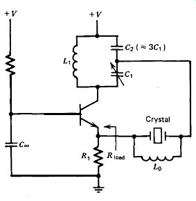
Figure 5.29. Common base circuit in Fig. 5.28 rearranged. Lo has been left
out for clarity.
the same time, the transistor's collector sees the L,C, tank as a (near) parallel-resonant
circuit of high impedance. Since the crystal wants to see a low source impedance
and the collector wants to see a high load impedance, both like what they see,
and the circuit ends up with a good impedance transformation ratio that depends
on the Q of the L,C, tank.
This explanation of circuit operation has been verified both experimentally
and analytically. Tuning the tank circuit depends almost entirely on L, and
C1 and is essentially independent of C,.
Does it make any difference if the crystal is tapped down on the inductor
in the LC tank instead of on the capacitor? Yes, it does. Figure 5.30 shows
an inductively tapped circuit. Tapping down on the inductor gives a phase lag
to the amplifier circuit, while tapping down on the capacitor gives a phase
lead. In both cases, there is a phase lag from the emitter to the collector,
caused by operating the LC tank off resonance.
The phase lead of a capacitor tap subtracts from the emitter-to-collector
phase lag and allows the crystal to oscillate either at or above series resonance.
The phase lag of an inductive tap just adds to the emitter-to collector phase
lag and forces the crystal to oscillate below series resonance, where it can
provide a phase lead to compensate the two other phase lags in the circuit
to zero. The end result is that a capacitive tap allows crystal operation above,
at, or slightly below series resonance, while the inductive tap allows crystal
operation only below series resonance. These phase-lead and phase-lag effects
are analyzed and discussed in detail in Sections 7.6 and 7.7.
Tapping into the capacitive side of the LC tank introduces a lot of parasitic
oscillations into the circuit. These parasitic oscillations are the biggest
drawback to the capacitive tap version of the circuit. Most, but
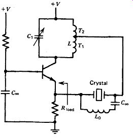
Figure 5.30.
Butler common base, inductive tap. L, is not needed below about 70 MHz. T2
is normally & to & of the total coil turns.
not all, of these parasitic oscillations can be suppressed by resistive loading
of the LC tank and careful attention to circuit layout. In contrast, the inductive
tap gives clean circuit operation without any parasitics and seems to give
equal frequency stability, but its oscillation frequency is about 4 ppm lower.
Another difficulty with Butler's common base circuit is that it will only
oscillate over a relatively narrow range of collector current. If the current
is too small, the circuit will not oscillate because loop gain is too low.
And if the current is too large, two undesirable things happen. First, the
collector's LC tank gets shunted with a low resistance from the large collector
current, which cuts the gain. And secondly, the emitter's input resistance,
which makes up most of the crystal's load resistance and is an inverse function
of the emitter current, becomes much smaller. This also cuts circuit gain,
so much so that the circuit will not oscillate.
A third difficulty is that it is hard to get the crystal drive voltage down
low enough to keep it from overdriving the emitter into cutoff and to keep
crystal dissipation within its limit. Figure 2.5 shows that the maximum drive
voltage for many crystals between 20-100 MHz at series resonance is 0.2 Vrms
or 0.6 Vp-p. We can tap down the crystal further on the LC tank in Figs. 5.28
or 5.29, but this reduces loop gain, which is already on the low side, and
the circuit may quit oscillating. One solution is to shunt the inductor in
the LC tank with two parallel diodes of reversed polarity, as shown in Fig.
10.17. This limits oscillation amplitude without cutting loop gain. Another
solution is to reduce the power supply voltage from 5 to 2 or 3 V.
For the Butler common base circuit to oscillate, experimental data indicate
that the impedance of the inductor L, in the LC tank in Fig. 5.28 should be
a certain fixed value (within a factor of 2 or so) regardless of the frequency.
This means that the inductive value of L, should vary inversely with frequency.
Table 5.2 lists some usable inductance values for L, at several frequencies
from 20 to 100 MHz. The inductance to be used at intermediate frequencies can
be interpolated from values given in Table 5.2. The circuit seems to work better
if the lower inductance value at each frequency is used.
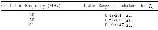
TABLE 5.2: Some Usable Inductance Values for the L1C1 Tank in the Butler Circuit
in Fig. 5.28.
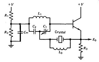
Figure 5.31. Butler emitter follower, capacitive tap. Lo is not needed at
frequencies below about 70 MHz.
5.14. HARMONIC-BUTLER EMITTER FOLLOWER
The Butler emitter follower is a VHF harmonic oscillator, operating at or
near series resonance; a basic schematic is shown in Fig. 5.31. The circuit
is useful mostly at frequencies between 20 and 200 MHz. The amplifier has a
gain of one; the oscillator's loop gain is provided by L, and C, operating
near series resonance. Tapping the crystal into the capacitive side of the
LC tank gives a phase lead, and the crystal then oscillates either at or slightly
above series resonance. Starting at 50-100 MHz, the impedance of the crystal's
terminal capacitance C,, (about 5 pF) approaches the crystal's series resistance
R, and provides an alternative path around the crystal, tending to short it
out. So above about 70 MHz, an inductor L, is tied across the crystal to parallel
resonate with the crystal's terminal capacitance C, and tune it out of the
circuit.
Although Butler's emitter follower circuit is not so well-known as .his common
base circuit, his emitter follower circuit offers many practical advantages
over the common base arrangement. Tapping down the crystal on the LC tank increases
the oscillator's loop gain instead of de creasing it, as in the common base
circuit. The amplifier's gain of one gives a stable gain configuration that
is independent of bias variations and always works with any transistor. The
emitter follower circuit can be operated at frequencies down to 1 kHz, whereas
the lowest frequency of the common base circuit is limited to about 8 or 10
MHz by the effect of the emitter's low load resistance on the crystal (high
gain loss).
The built-in feedback of an emitter follower circuit gives a very wide amplifier
bandwidth, allowing the circuit to operate at higher frequencies than what
the common base circuit will provide. There are no parasitic oscillation effects
because of the amplifier's low gain of one and its built-in feedback stabilization.
Compared to the common base amplifier, the undesirable oscillation damping
provided by DC current flow through the inductor is reduced by the transistor's
current gain hfe of 20-100. And while loop gain drops slightly with a heavy
emitter current, the emitter follower is not limited to a narrow operating
current range, as is the common base circuit. At any given frequency, a wider
range of inductance values can be used with the emitter follower circuit than
with the common base arrangement.
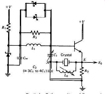
Figure 5.32. Practical Butler emitter follower circuit.
A practical Butler emitter follower is shown in Fig. 5.32. It operates as
follows: L,C, form a resonant circuit operating near (but not at) series resonance,
providing a low input impedance to the crystal and a high output impedance
to the transistor base. All of the oscillator's loop gain comes from L; and
C, operating near series resonance. The value of C, has almost no effect on
the resonant tuning of the LC tank circuit, which seems to be due to the shunting
effect of the crystal's low impedance on c,.
From the emitter's viewpoint in Fig. 5.32, C, is effectively in series with
the crystal, which raises the oscillation frequency slightly above series resonance.
It is desirable to make C, large in order to give it a low impedance, which
moves the oscillation frequency down closer to series resonance. There is an
optimum value for C,: If C, is too large, it short circuits the amplifier gain
loop and cuts the gain. If C, is too small, it starts reacting with the inductive
input impedance of L1C1 raising the crystal's load impedance to an undesirably
high value. The optimum impedance of C, is about 0.5-1 times the crystal's
series resistance R,.
R, gives the emitter follower a low output resistance for driving the crystal
load. The two Schottky diodes across L, limit oscillation amplitude to (1)
keep the crystal's power dissipation within its rating and (2) keep the transistor
conducting over the complete oscillation waveform and maintain a low emitter
drive resistance for the crystal over a complete cycle. The crystal's load
capacitor C, is tied to the grounded end of the emitter resistor R, rather
than to the Zener bias supply, as was shown in Fig. 5.31. Tying C, to the grounded
end of R, gives a shorter crystal drive loop from the emitter, and the circuit
performs better. The base bias voltage is stabilized with a Zener diode to
reduce frequency shift when the power supply voltage changes. This bias stabilization
reduces frequency sensitivity to power supply changes by an order of magnitude.
Selection of L and C values is as follows: C, is selected so that its reactance
is equal to about 0.5 to 1 times the crystal's series resistance.
C, should be 1/3 to 1/4 of C,. If C, is one-half of C,, the crystal's load
impedance is undesirably high; if C, is one-eighth of CB, loop gain is too
low. L, is selected for approximate series resonance with C,. There is an experimental
cross-check on the correct values of C, and C,. In Fig. 5.32, C 1 and C, are
in the right range when voltage at point A is 30-70% of the voltage at point
E, indicating that the crystal's load impedance is approximately equal to the
crystal's internal impedance.
Figure 5.33 shows an alternative emitter follower circuit with the A 5 T Figure
5.33. Butler emitter follower, inductive tap. T2 is normally $ to B of the
total coil turns.
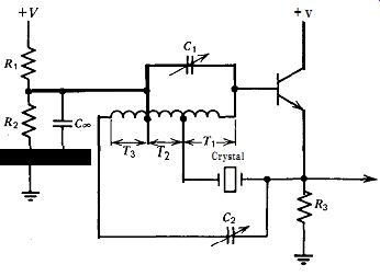
Figure 5.34. Alternative compensation scheme for crystal's shunt terminal
capacitance Co.
crystal tapped into the inductive side of the LC tank circuit rather than
into the capacitive side. T, is set at about 'Is to % of the total turns on
the inductor. This provides a phase lag in the amplifier circuit loop, and
the crystal then oscillates either at or slightly below series resonance. The
L and C circuit values are selected on a basis similar to that used for the
capacitive tap circuit.
Figure 5.34 shows an alternative scheme proposed by Butler [6] to compensate
for the crystal's terminal capacitance C,. Above 50-100 MHz, the crystal's
shunt terminal capacitance C, provides an undesirable shunt path around the
crystal's internal frequency-controlling elements. Rather than resonating an
inductance L, in parallel with Co, the idea here is to cancel the effects of
C,, by adding an equal voltage of opposite phase through an equivalent capacitance
C, to the LC tank. The reversed phase is obtained by extending the inductance
winding in the LC tank below AC ground. The emitter signal is then fed to this
reversed polarity terminal through a capacitance C,. If T2 = T3 and C2 = C,,
(the crystal's shunt capacitance), then the shunt signal through the crystal's
capacitance is canceled out. One drawback to this arrangement is the increased
capacitive loading on the emitter, which is already heavily loaded by the crystal
impedance. As will be shown in Section 10.24, this compensation scheme does
not work out very well in practice.
Prev. | Next | Index
|
Home |
This page was last updated: Friday, 2007-07-20 17:18,Monday, 2023-07-24 18:21
PST