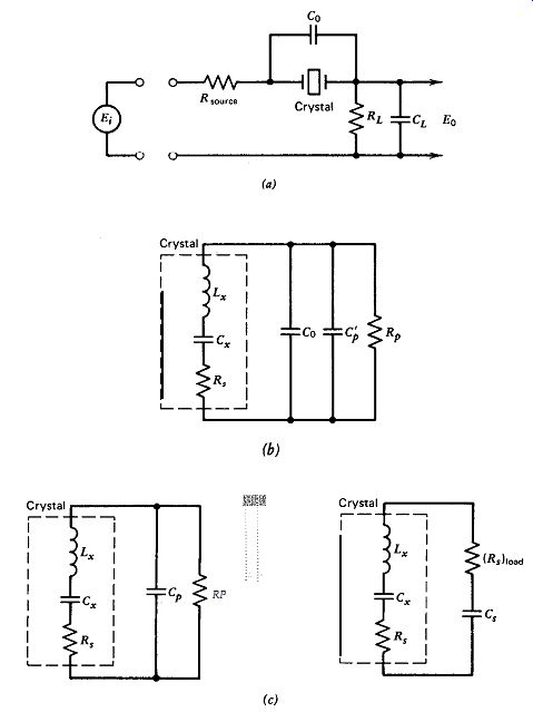
Figure 6.1. Equivalent crystal RC load circuits in both series (R,)load C, and parallel R,C, load forms: (a) typical crystal load circuit, (b) intermediate load circuit, and (c) equivalent load circuits.
| Home | Audio mag. | Stereo Review mag. | High Fidelity mag. | AE/AA mag. |
This section shows the relationship between short-term frequency stability and in-circuit Q. Section 6.1 describes the effect of the crystal's external load resistance on in-circuit Q and useful differences between series and parallel equivalents of a combined resistive-capacitive load on a crystal. Section 6.2 presents experimental data showing that the equivalent series resistance of the crystal load is the component to be minimized for maximum short-term frequency stability and shows what values of parallel-load resistance will give good in-circuit Q.
6.1. IN-CIRCUIT
[…] oscillation loop. To minimize Q losses, we can keep the crystal's external load resistance relatively low; that is, equal to or less than the crystal's internal series resistance R,, so that the in-circuit Q is not degraded by more than a factor of two from the crystal's internal Q. Another approach is to use a reactive load (which is lossless) rather than a resistive one. An example of this is the Pierce circuit, where the external load on the crystal is primarily capacitive rather than resistive. A third approach, which is not widely known, is to use a load resistance that is very large with respect to the reactance of the crystal's terminal shunt capacitance C_O, so that the external crystal load is effectively capacitive (and low loss) rather than resistive. In general, the technique of using a reactive load on the crystal instead of a resistive one is very effective in obtaining a high in-circuit Q and improves short-term frequency stability.
In describing the load on a crystal, it is important to distinguish between two equivalent representations, that is, as a parallel load with resistance and capacitance in parallel with each other or as an equivalent series load with resistance and capacitance in series with each other. For maximizing in-circuit Q, it turns out that we want to minimize the equivalent series load resistance, as is shown in the next section.
Figure 6.1 shows a commonly used crystal circuit, with source and load resistances, load capacitance, and the crystal's shunt terminal capacitance C_o indicated. From the crystal's point of view, the load impedance across the crystal's terminals is in series with its internal L, and C, components, as shown in Fig. 6.lb. Hence, a reactive load impedance on the crystal will change the resonant frequency by changing the net total series inductance and/or capacitance in the crystal's oscillation loop. It is also apparent from Fig. 6.lb that from the viewpoint of the crystal's internal frequency controlling elements L, and C,, the crystal's shunt terminal capacitance C,, should be considered as part of the load on the crystal, and not as part of its internal frequency-controlling elements.
From the crystal's viewpoint, it is easier to use the equivalent series RF, load network for determining in-circuit Q, as shown in the right-half of Fig. 6.1. But from a circuit-design viewpoint, it is easier to use the parallel R,C, load network, as shown in the left-half of Fig. 6.1. To tie the two viewpoints together, we need to do some parallel to series (and vice versa) conversions of the crystal's load impedance.
The minimum value of C, is the crystal's shunt terminal capacitance C0, about 5 pF. Using a fixed value of 5 pF for C, and a l-MHz oscillation frequency, Fig. 6.2 shows equivalent series values of (Rs) load and C, for various values of parallel load resistance R,. To maximize the crystal's in-circuit Q, we should minimize (R8 load ) in the right-half of Fig. 6.1.
Figure 6.1. Equivalent crystal RC load circuits in both series (R,)load C,
and parallel R,C, load forms: (a) typical crystal load circuit, (b) intermediate
load circuit, and (c) equivalent load circuits.
Figure 6.2 shows that either low or high values of R, will give acceptably low values of (Rs)load but that intermediate values of R, near 32K R will give unacceptably high values of (Rs)load, with a resulting very low in circuit Q.
By converting equivalent values of (Rs) load into circuit Q, where 2 pi (frequency) L,
Crystal parallel load resistance, Rp In)
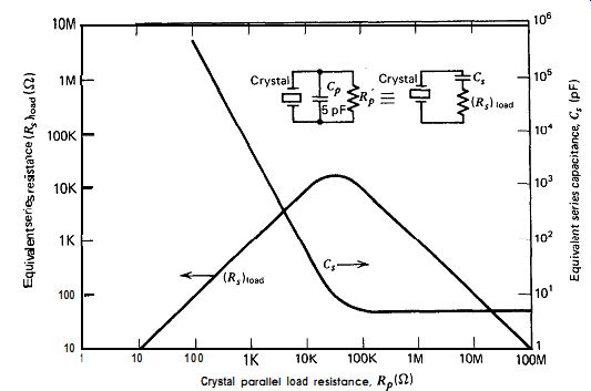
Figure 6.2. Equivalent series (R,)load
and C, values for a parallel R,C, network at 1 MHz. C, is fixed at 5 pF,
R, is varied from 10 ohm to 100 MO.
Fig. 6.3 shows the variation of circuit Q with parallel load resistance R,.
Figure 6.3 shows that circuit Q is high for both low and high values of R, but very low for R, values anywhere near 32K R. In fact, for circuit Q to be half or more of its maximum value, R, has to be more than two orders of magnitude higher or lower than 32K a. What is happening at 32K-o At 32K-o, parallel resistance R, is equal to the 32K reactive impedance of parallel capacitance C,. And when that occurs, the transformation of R, into its equivalent series value (Rs) load gives a peak in the series resistance value (Rs) load, as shown in Fig. 6.2.
Since all quartz crystals have a shunt terminal capacitance C0 of about 5 pF, we can generalize this parallel-to-series peaking effect to any frequency by saying that for good in-circuit Q the parallel load resistance R, should be greater or less than the reactance of the crystal's terminal capacitance C, by two orders of magnitude. Figure 6.4 is a graph of this relationship, showing good and bad values of parallel resistance R, for both low and high values of circuit Q. The average value for the crystal's terminal capacitance C, was 5 pF, which, with assumed zero load capacitance CL, is equal to parallel load capacitance C,. This calculated relationship between parallel load resistance R, and in-circuit Q is verified by experimental data in the next section.
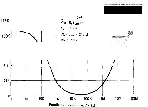
Figure 6.3. Calculated in-circuit Q versus crystal parallel load resistance
RP.
6.2. MEASUREMENT OF IN-CIRCUIT Q
There are many ways to measure in-circuit Q. The method used here is to suddenly disconnect the crystal from the oscillator circuit and measure the decay of the voltage across the crystal (or the current through it) as a function of time. The measurement of Q is taken as the time required for the voltage across the crystal (or the current through it) to decay to 1/e of its initial value. The longer the decay time, the higher the Q.
Figures 6.5 and 6.6 show the envelope of voltage decay across a 1-MHz crystal for various resistive and capacitive loads across the crystal terminals. Loads range from a near open circuit to a short circuit. All waveforms shown are voltage measurements across the crystal except for the short-circuit measurement, which is a current measurement using a Tektronix current probe. The impedance of the current probe is about 0.1 R. A mechanical toggle switch was used for switching the crystal out of the circuit, and the bounce of the switch contacts can be seen at the left edge in some of the photographs. Note, in particular, in Fig. 6.5 the very fast decay with a 10K ohm resistive load on the 1-MHz crystal.
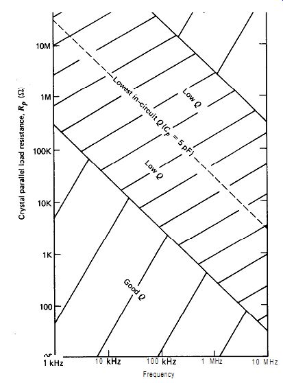
Figure 6.4. Calculated in-circuit Q versus crystal parallel load resistance
R, as a function of frequency.
If we measure the crystal's relative Q, as indicated by decay rates in the photographs in Figs. 6.5 and 6.6 and plot it as a function of load resistance and capacitance, we obtain the curves shown in Figs. 6.7 and 6.8. Figures 6.7 and 6.8 also show curves of relative crystal Q at four other frequencies: 4,50, and 100 kHz, and 10 MHz. In order to show all five frequencies, the ordinates in Figs. 6.7 and 6.8 are not plotted in terms of decay time to 1/e their initial value but in terms of the total number of oscillation cycles that occur during the 1/e decay time. It is probably more relevant to plot the curves this way as well as more convenient.
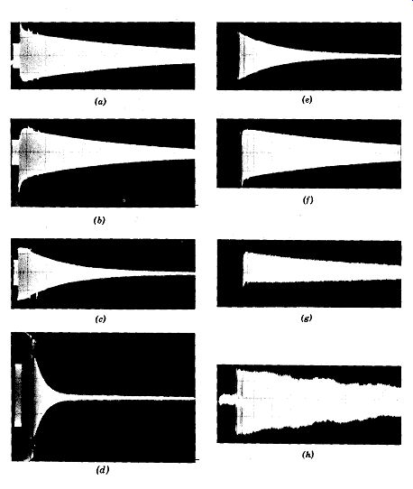
Figure 6.5. Crystal voltage (current) decay as a function of crystal load
resistance. All waveforms with same time base of 2 m-sec/div and crystal disconnected
from oscillator circuit. Vertical voltage scales vary. See Fig. 6.11~ for test
circuit used to obtain these waveforms. (a) 10 Ma, (b) 1 MR, (c) 100 K& (d)
10 KR, (e) 1K R, (f) 100 a, (g) 10 R, and (h) 0 R (short circuit).
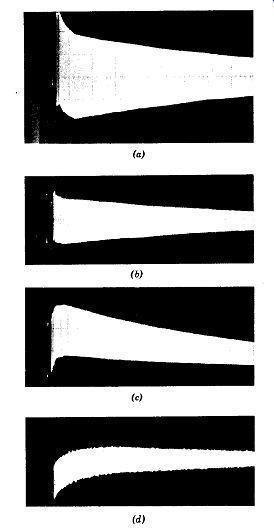
Figure 6.6. Crystal voltage decay as a function of crystal load capacitance.
All waveforms with same time base of 2 msec/div and crystal disconnected from
oscillator circuit. Vertical voltage scales vary. See Fig. 6.11a for test circuit
used to obtain these waveforms. (a) 40 pF, (b) 200 pF, (c) 2000 pF, and (d)
20,000 pF.
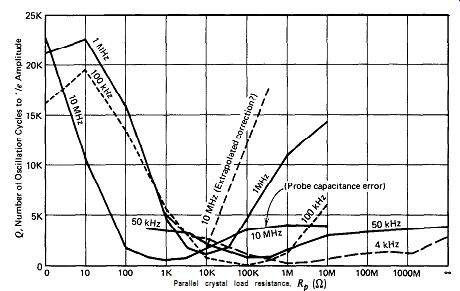
Figure 6.7. Measured crystal Q versus parallel load resistance R, across the
crystal terminals. C, = 10-20 pF.
The Q curve at 10 MHz in Fig. 6.7 contains a measurement error at the high load resistance values, due to the 7 pF of shunt capacitance in the scope probe used. The shunt impedance of the 7 pF of probe capacitance is 3000 R at 10 MHz, which completely swamps out the effect of any high resistance values in parallel with it across the crystal. Without the loading of the probe's shunt capacitance, the Q curve of the lo-MHz crystal would probably look more like the dotted line shown in Fig. 6.7.
These experimental curves of crystal Q versus loading in Figs. 6.7 and 6.8 provide considerable information. First, capacitive loading in general gives a higher Q than resistive loading. Second, the best Q is obtained with the crystal short circuited. Third, each of the resistive loading curves in Fig. 6.7 shows a minimum Q at the middle values of resistive loading, and, in each case, parallel resistive loading R, on the crystal must be increased or decreased by about two orders of magnitude away from the resistance value at minimum Q to get good circuit Q. Figure 6.9 shows these minimum Q resistance values plotted as a function of frequency. Two additional lines have been drawn in Fig. 6.9, which are parallel to the minimum Q line but displaced from it by two orders of magnitude in the parallel load-resistance value. Figure 6.9 shows graphically what resistance-loading values on the crystal will give both good and poor in-circuit Q at any frequency.
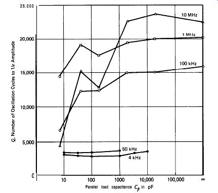
Figure 6.8. Measured crystal Q versus parallel load capacitance C, across
the crystal terminals. R, = 10-1000 M-o.
Comparing experimental data in Figs. 6.7 and 6.9 with the calculated data in Figs. 6.3 and 6.4, we see that they are the same except that the experimental values of parallel load resistance are lower than the calculated values by a factor of three at all frequencies. One difference between calculated and measured data is that the calculated value of parallel capacitance C, is 5 pF while the experimental value is 15 pF, as defined by the impedance of the line of lowest Q in Fig. 6.9. The 15 pF consists of 5 pF of crystal terminal capacitance Co plus 7 pF of scope probe capacitance plus 3 pF of stray capacitance. This 3 to 1 difference between the calculated and experimental values for the parallel load capacitance C, would shift the experimental values of parallel load resistance downward by a factor of three, and this is exactly what a comparison of Fig. 6.9 with Fig. 6.4 shows. The experimental data thus confirms that the low Q at medium resistance values is due to converting
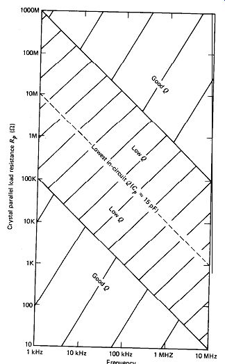
Figure 6.9.
Measured effect of a parallel resistive crystal load R, on Q as a function
of frequency.
the parallel RC load values to their equivalent series values. R,, (Rs)load, CP, and C, are defined in Fig. 6.1.
The calculation and measurement of the effects of various loads on crystal operation show the following:
1. The load tied across the crystal's terminals, has a strong effect on the crystal's in-circuit Q.
-----
-------
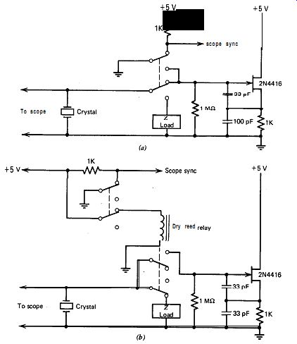
Figure 6.11. Test circuits for measuring crystal loading effects on in-circuit
Q:
(a) at 1 MHz and (b) at 10 MHz.
The test circuits used for measuring the effects of loading on crystal Q are given in Figs. 6.10 and 6.11. In the 10-MHz test circuit, a dry reed relay rather than a mechanical switch was used to switch the crystal, since the contact bounce time of a manually operated switch was excessive at this frequency.