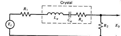
Figure 7.1. Resistive load on crystal:
| Home | Audio mag. | Stereo Review mag. | High Fidelity mag. | AE/AA mag. |
For an oscillator to oscillate, the total phase shift around the oscillator loop has to be 0 degr, 360 degr, or some multiple of 360 degr. If the total phase shift around the loop changes slightly, the oscillation frequency moves up or down until the total phase shift is again back at 0 degr., 360 degr., or some multiple of 360 degr. The greater the rate of phase change with frequency, the less the frequency has to shift to drive the phase back to its null point. This correlates directly with circuit Q and the circuit's short-term frequency stability.
LC networks in the loop that are isolated from the crystal do not change phase with frequency fast enough to have any effect on short term stability. LC networks directly connected to the crystal do have an effect on the rate of phase change with frequency, primarily because they can be used to short out or hide resistive sources and loads from the crystal.
In the following sections, various crystal circuit configurations and load conditions are analyzed for gain and phase changes with frequency.
The intent is to maximize the phase change with frequency, since this is what gives short-term stability to an oscillator.
For brevity, derivations of gain and phase-shift equations for the circuits are not shown, and only analytical results are given. The circuit equations are derived as follows. Each circuit consists of one to three interconnected loops of RLC components. An equation is written for each loop, using standard circuit analysis techniques, and steady state conditions are assumed. These equations are then solved as a simultaneous set of linear equations for the circuits' gain and phase-shift transfer functions of:
| E_o / E_i | and E_o/E_i
[…] frequency. Since everything of interest happens near the crystal's series resonant frequency, the plotted data curves are limited to frequencies near series resonance, with the frequency scale marked in parts-per million (ppm) deviation from the crystal's series-resonant frequency.
The analysis has been simplified by ignoring the shunt capacitance C, across the crystal's case terminals, which limits the validity of the analysis to what happens near series resonance. The analytical curves shown were programmed and calculated on a TI-59 calculator. To help make comparisons between circuits, all phase and amplitude curves are plot ted to the same scale, and the same 1-MHz crystal values are used in all the fundamental circuits. For the VHF harmonic circuits, the same 20 MHz third harmonic crystal values are used in all of those circuits.
7.1. RESISTIVE LOAD ON CRYSTAL
A circuit with a resistive load on the crystal is shown in Fig. 7.1, with typical circuit values listed. Figure 7.2 shows the circuit's phase shift E_o/E_i
… as a function of frequency. These curves are typical for a reasonably small resistive load on the crystal. Although not shown, if source and load resistances are increased, the rate of phase change with frequency decreases, indicating poorer short-term frequency stability. If source and load resistances are decreased, the rate of phase change with frequency increases, indicating better short-term frequency stability.
The maximum phase change with frequency occurs with zero source and load resistances. Assuming no phase shift in the amplifier, this circuit will oscillate exactly at series resonance.
7.2. CAPACITIVE LOAD ON CRYSTAL
A circuit with a capacitive load on the crystal is shown in Fig. 7.4, with typical circuit values listed. Figure 7.2 shows the circuit's phase shift
Figure 7.1. Resistive load on crystal:
Frequency = 1 MHz; L, = 4.2 H; C,. = 0.006031228 pF; R, = 240R; 23, = 120i-l; R, = 120R.
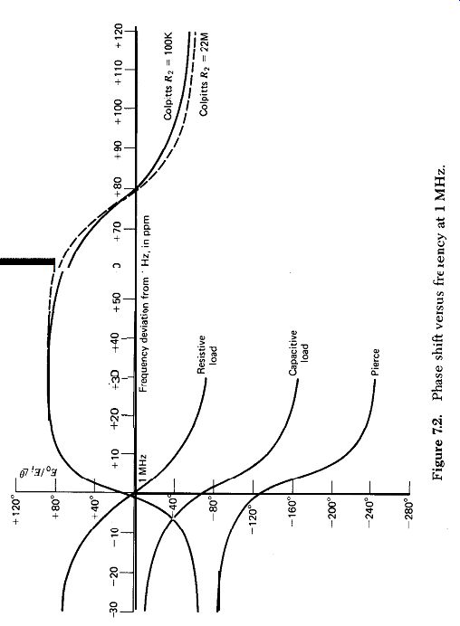
Figure 7.2
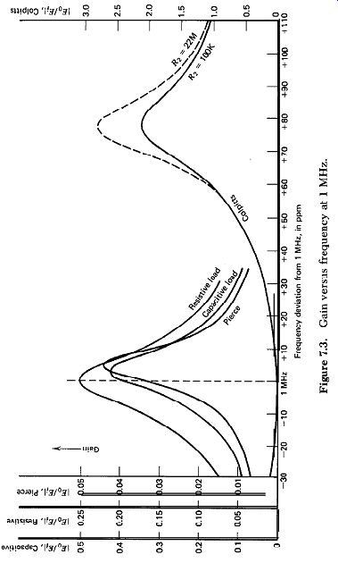
Figure 7.3
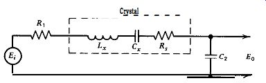
Figure 7.4. Capacitive load on crystal: Frequency = 1 MHz; L, = 4.2 H; C,
= 0.0060310228 pF; R, = 240 R; R, = 120 R; C, = 1000 pF.
E_o/E_i
…. versus frequency. Note that in Fig. 7.2 the phase slope is greater with a capacitive load than a resistive load on the crystal.
The general idea is to try to use these circuits where the phase slope is the steepest. With the capacitive load this occurs at 3 ppm above the l-MHz series-resonance frequency. The phase shift through the network at this frequency is a 90 degr. lag. Amplifiers usually have a phase shift of 0 degr. or 180 degr. So if this capacitive load circuit is to be used in an oscillator, an other 90 degr. phase-shift network should be added to the circuit either to increase the phase shift to 180 degr. or decrease it to 0 degr., depending on whether the amplifier is inverting or noninverting.
7.3. PIERCE CIRCUIT
A simplified Pierce circuit (without amplifier) is shown in Fig. 7.5. An explanation of how this circuit works is given in Section 5.8 and will not be repeated here. The phase shift of this circuit from input to output E_o/E_i is shown in Fig. 7.3. Figure 7.2 shows that if this circuit is used with a 180 degr. inverting amplifier, it will oscillate about 6 ppm above series resonance.
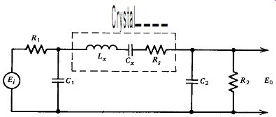
Figure 7.5. Simplified Pierce circuit: Frequency = 1 MHz; L, = 4.2 H; C, =
0.0060310228 pF; R, = 240 R; R, = 1000 a; R, = 1000 R; C, = 0.001 pF; c2 =
0.002 pF.
The phase slope is higher than either the resistive or capacitive load circuits in Fig. 7.2, indicating that it will have better short-term frequency stability than either of those circuits. Note that in Fig. 7.5 capacitors C, and C, tend to short out source and load resistances, raising the crystal's effective in-circuit Q. It is this shorting-out factor that gives the Pierce circuit its high phase slope with frequency and the very good frequency stability that goes with it.
7.4. COLPITTS CIRCUIT
A simplified Colpitts circuit (without amplifier) is shown in Fig. 7.6. As mentioned in Section 5.3, the Colpitts has three different operating states: transistor on, transistor saturated, and transistor shut off. The longest of the three states occurs when the transistor is shut off, so the shut-off stage was picked as the most typical and is the one shown in Fig. 7.6. The phase shift (E_o / E_i) i is shown in Fig. 7.3.
The solid curves in Figs. 7.2 and 7.3 represent a transistor-Colpitts, where the crystal's load resistor R, is the transistor's base bias resistor of 100K a. The dotted curves represent a FET-Colpitts circuit, where the crystal's load resistor R2 is the FET's gate-to-ground resistor of 22 M-ohm.
The circuit's actual frequency stability is better than the low slope of the phase shift curve in Fig. 7.2 would indicate, which means that the transistor shut-off state shown in Fig. 7.6 is a poor average of the three states in the actual circuit. Improving the simplified circuit's accuracy requires including the other two states of operation. This requires a large effort. It c2 ==
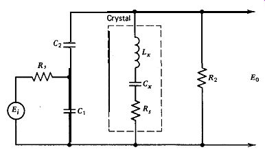
Figure 7.6. Simplified Colpitts circuit: Frequency = 1 MHz; L, = 4.2 H; C,
= 0.0060310228 pF; R, = 240R; R, = 2KR; R2 = 100KR; C, = 220 pF; C2 = 47 pF.
is necessary to match the boundary conditions of the three operating states and the results are not considered worth the effort.
However, the phase shift curve in Fig. 7.2 is correct in showing that the oscillation frequency is a high 79 ppm above series resonance (the actual oscillation frequency measured in the 1 MHz transistor-Colpitts circuit was 94 ppm above series resonance). Note that the phase shift curve in Fig. 7.2 shows 0 degr. phase shift at two frequencies where oscillation could occur, but that the amplitude curve in Fig. 7.3 shows that only the higher frequency of 79 ppm above series resonance has enough gain (i.e., >l) for oscillation to occur.
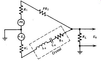
Figure 7.7. Modified Meacham half-bridge circuit: Frequency = 1 MHz; L, =
4.2H;C,=0.0060310228pF;R,=240R;R,=8R;R;=8~;R,=2000~;~=1,
0.5, 0.25, 0.125; R2 = 240, 480, 960, 1920R.
7.5. MODIFIED MEACHAM CIRCUIT
The modified Meacham half bridge circuit is shown for analysis in Fig. 7.7. The coefficient P allows various bridge excitation ratios between the split-load phase inverter's emitter and collector voltages. When the bridge's excitation ratio P is changed, the bridge resistor PR, is changed proportionately with respect to the crystal's internal series resistance R, in order to maintain bridge balance.
The emitter and collector source resistances R; and R, have different resistance values when measured independently with respect to ground.
The two source resistances have the same resistance value, however, if measured with a load tied between them rather than from each point to ground. The source resistances are equal even if the phase inverter's emitter and collector resistors (R; and R,) are not equal.
The capacitances shunting the two bridge arms are nominally balanced to the bridge null. For simplicity, they are left out of the analysis, since they are primarily important for high-frequency stability reasons in this circuit and have little effect on oscillation frequency. The omission limits the accuracy of the analysis, but the intent here is to show only the general amplitude and phase characteristics of the bridge.
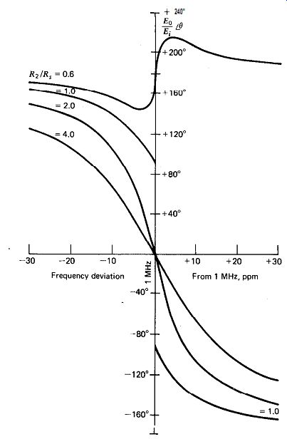
Figure 7.8. Bridge phase shift versus frequency for several amounts of imbalance
from null. Bridge excitation ratio P = 1 for all curves.
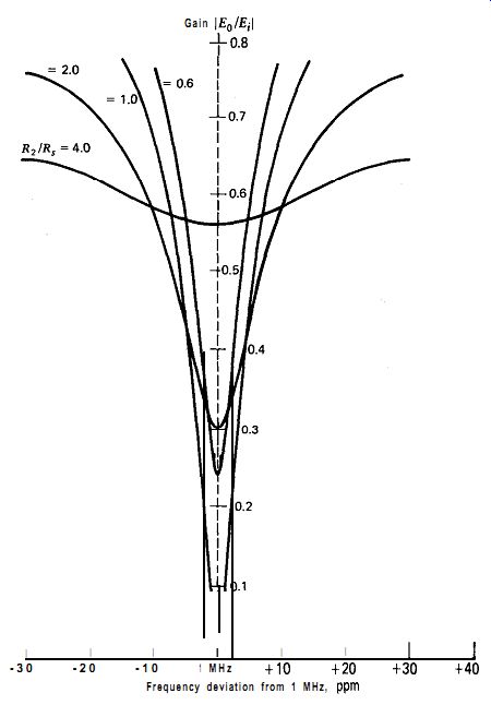
Figure 7.9. Bridge gain versus frequency for several amounts of imbalance
from null. Bridge excitation ratio P = 1 for all curves.
Figures 7.8 and 7.9 show the phase shift (Eo/Ei) of the modified Meacham half-bridge circuit for various amounts of bridge unbalance. Both bridge arms have equal excitation voltages (P = 1). The only changes in the curves occur near the crystal's resonant frequency (1 MHz, in this case), so only the circuit's response at frequencies near resonance is shown. The curves are plotted in terms of the bridge imbalance ratio R,/R,. When R,/R, = 1, the bridge is balanced with zero output from the bridge at resonance, as shown in Fig. 7.9. At frequencies away from resonance, the output amplitude approaches the input amplitude regardless of the amount of imbalance.
The phase shift through the bridge varies from + 180 degr. at low frequencies to 0 degr. at resonance to - 180 degr. at high frequencies. The one exception to this phase characteristic is when the ratio R2/RS, is less than one, and then the phase shift through the bridge stays near +180 degr. at all frequencies.
The circuit will not oscillate (except parasitically) when R2/RS, is equal to or less than one, so the useful phase curves are those with a ratio of R2 / R1 greater than one.
The steeper the slope of the phase shift curve in Fig. 7.8, the better the short-term frequency stability will be, since a smaller frequency change is then needed to provide any given amount of phase-angle correction and maintain the total phase shift around the oscillator loop at 0 degr. (or 360 degr.). To provide a comparison, the Pierce circuit's phase shift (Fig. 7.2) falls about halfway between the two phase-shift curves R2/RS, = 2 and R2/RS, = 4 in Fig. 7.8 or at about R2/RS, = 3. Thus, by operating the Meacham half-bridge with a R2/RS, ratio 'less than three, we should get a short-term stability better than that of the Pierce circuit. The Meacham circuit can be operated with a R2/RS, ratio of less than three (a ratio of 1.0 is the theoretical limit) by the simple expedient of increasing the oscillator's amplifier gain. In practice, this is not so simple, since the tendency for parasitic oscillation increases when the gain is increased.
There are advantages to operating the Meacham half-bridge with un equal excitation voltages (I' # 1) to the two bridge arms. In particular, it is advantageous for the excitation voltage driving the crystal to be larger than the voltage driving R,. These advantages are described in detail in Section 5.11. Figures 7.10 and 7.11 show the bridge's phase shift (Eo/Ei) functions for several values of P, the bridge excitation ratio.
All of the curves in Figs. 7.10 and 7.11 use the same bridge-imbalance ratio R2/RS, = 2. This imbalance ratio is typical of the actual Meacham circuits described later in Sections 10 and 11. The curves show that changing the excitation ratio does not change the phase curve much, but it does change the amplitude curve considerably, particularly at frequencies away from resonance. At frequencies away from resonance, the bridge's gain, or amplitude ratio, 1 Eo/Ei ) decreases in direct proportion as the excitation ratio P is decreased, which helps considerably in reducing parasitic oscillations.
The exact amount of bridge imbalance is slightly different in each of the four curves in Figs. 7.10 and 7.11, since the source resistances R, and R: do not change with P. The effect of the difference on the curves is relatively small. The biggest effect is a 16% reduction in the gain curves in Fig. 7.11 at the frequency of resonance (1 MHz).
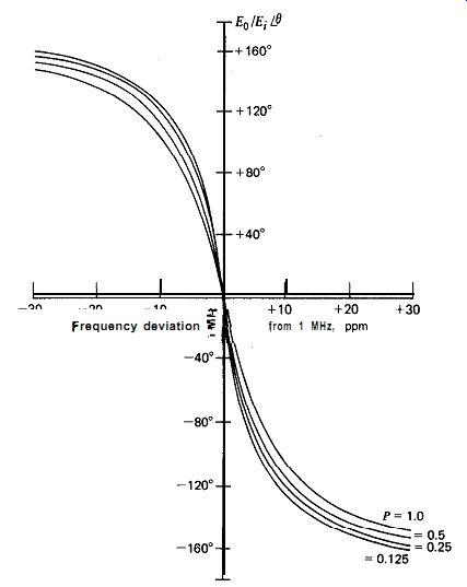
Figure 7.10. Bridge phase shift versus frequency for several values of bridge
excitation ratio P. The bridge has a fixed null imbalance of R2/RS, = 2 for
all curves.
7.6. BUTLER HARMONIC CIRCUITS, C-TAP
The capacitive tap versions of Butler's emitter follower and common base oscillator circuits are shown in Figs. 7.12 and 7.13. These two circuits are analyzed together, since analytically they are the same circuit, one being the reverse of the other. The one difference between them is the gain 1 Eo/Ei 1, which peaks at about 2.3 maximum for the emitter follower circuit and at about 0.035 maximum for the common base circuit.
Phase shifts are the same, gain curve shapes are the same, and the crystal's source impedance Z, in one circuit is the crystal's load impedance Z, in the other. The notation of the emitter follower circuit will be used here for convenience, since its amplifier has a known gain of one with zero phase shift, which makes the gain and phase curves easier to under stand and interpret. The oscillation frequency used is 20 MHz, since this is the lowest frequency that this circuit is likely to be used at.
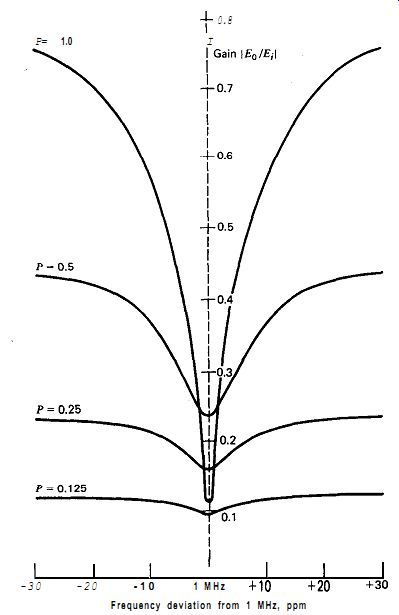
Figure 7.11. Bridge gain versus frequency for several values of bridge excitation
ratio P. The bridge has a fixed null imbalance of R2/RS, = 2 for all curves.
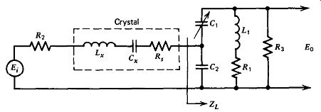
Figure 7.12. Butler emitter follower, capacitive tap.
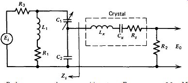
Figure 7.13. Butler common base, capacitive tap: Frequency = 20 MHz; L, =
0.053 H; C, = 0.0011948253 pF; R, = 30 fl; R, = 0.02-0.45 a; R2 = 15 R; R3
= 1000 0; C, = 12-448 pF; C2 = 150,330,680 pF; L, = 0.25-4.0 CLH.
The crystal's load impedance is primarily determined by C,. C, is normally selected so that its impedance is approximately equal to or a little less than the crystal's internal series resistance R,. For analysis purposes, three values of C, are selected-one whose impedance is lower than R,, one approximately equal to R,, and one higher than R,. For each value of C$, three values of L, are selected, with the middle value of L, in each case selected to give near maximum circuit gain. This gives nine sets of data, which are sufficient to show the effects of the different circuit components. These nine data sets are plotted in Figs. 7.14, 7.15, and 7.16 and show the following results:
1.
2.
3.
4.
5.
Circuit loop gain varies with frequency, L,, and Cr. For any given value of C2, there is an optimum value of C, for maximum circuit gain, Maximum circuit gain occurs when L, is selected to give a C,/C, ratio of about 4.
Oscillation is generally slightly above series resonance but can be set exactly at series resonance by tuning C, to the right value.
The impedance of C, must be equal to or less than the crystal's internal series resistance R, if the crystal's load impedance is to be kept reasonably small.
The frequency of oscillation is relatively insensitive to the value of C2. Making C, smaller moves the oscillation band slowly up ward and farther away from series resonance.
Slopes of the better phase shift versus frequency curves are reasonably high, indicating that good short-term frequency stability can be obtained by selecting the right component values.
Frequency deviation from 20 MHz, in ppm Figure 7.14. Gain versus frequency for Butler circuits, C-tap.
All five of these analytical results have been observed experimentally in the test circuits. It may be helpful to explain how data in Figs. 7.14,7.15, and 7.16 were calculated. Oscillation occurs at that frequency where the phase shift through the network is zero. For a given set of circuit values, the frequency of zero phase shift (i.e., the frequency of oscillation) is varied by tuning C i over a range of values. The gain through the circuit at each frequency of zero phase shift (E,lE,) /rB is plotted in Fig. 7.14 as a function of the oscillation frequency. The crystal's load impedance 1 ZL 1 is plotted in Fig. 7.16 as a function of the oscillation frequency, under the same condition of zero phase shift through the circuit.
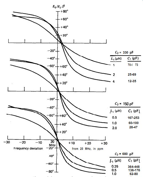
Figure 7.15. Phase shift versus frequency for Butler circuits, C-tap.
For the plots of phase shift ( Eo/Ei) 1 are held fixed, since we are interested here in how large a phase-angle correction is generated if the oscillation frequency were to deviate slightly from the frequency of zero phase shift. The frequencies at which the phase shifts were calculated were at the peaks of the gain curves shown in Fig. 7.14. Any part of the gain curves in Fig. 7.14 could have been used, however, since phase shift calculations at other frequencies across the gain curves all showed the same rate of phase change with frequency.
7.7. BUTLER HARMONIC CIFWJITS, L-TAP
Inductive tap versions of Butler's emitter follower and common base amplifier circuits are shown in Figs. '7.17 and 7.18. The two circuits are analyzed together, since analytically they are the same circuit, one being the reverse of the other. The one difference between them is the gain 1 Eo/Ei ( , which peaks at about 2.3 maximum for the emitter follower circuit and at about 0.035 maximum for the common base circuit. Phase shifts are the same, gain curves are the same, and the crystal's source impedance 2, in one circuit is the crystal's load impedance ZL in the other. The notation of the emitter follower circuit will be used here, since its amplifier has a known gain of one with zero phase shift, which makes the calculated gain and phase curves easier to understand and interpret. The oscillation frequency used is 20 MHz, since this is the lowest frequency at which this circuit is likely to be used.
Frequency deviation from 20 MHz. in ppm
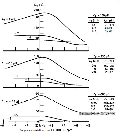
Figure 7.16. Crystal load impedance versus frequency for Butler circuits,
C-tap,
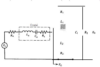
Figure 7.17. Butler emitter follower, inductive tap.
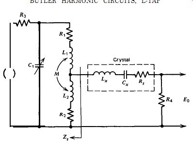
Figure 7.18. Butler common base, inductive tap: Frequency = 20 MHz; L, = 0.053
H; C, = 0.0011948253 pF; R, = 30 a; R, = 0.01-0.41 a; R, = 0.004-0.036 R; R3
= 1000 R; R, = 15 fl; C, = 7-270 pF; K = M/a = 0.12; Z,,. = 0.14-3.45~ H; L,
= 0.08,0.15,0.30~ H; M = .013-0.122~ H; Ltota, = L, + L, + 0.25-4.0pH.
The crystal's load impedance is primarily determined by L,, the inductance of the tapped portion of the inductor, as shown in Figs. 7.17 and 7.18. Normally, L, is selected so that its impedance is approximately equal to or a little less than the crystal's internal series resistance R,. For analysis purposes, three values of L, are selected, whose impedances are lower than R,, approximately equal to R,, and higher than R,. And for each value of L,, three inductance values for the whole inductor L_total are selected, with the middle value selected in Each case to give near maximum circuit gain. This gives nine sets of data, which are sufficient to show the effects of different circuit components. The single-layer air core Miller coils used in the test circuits had an average coefficient of
Frequency deviation from 20 MHz, in ppm
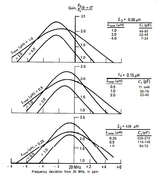
Figure 7.19. Gain versus frequency for Butler circuits, L-tap.
coupling K (K = M/a) of 0.12. This coefficient was used to specify mutual inductance M between the two parts of the solenoid coil L, and L Analytical data are plotted in Figs. 7.19, 7.20, and 7.21 and show the following results:
1. Circuit gain varies with frequency, L1, and Cr. For any given value of L,, there is an optimum value of L, for maximum circuit gain.
Maximum circuit" gain occurs when the crystal is tapped into the coil at about % of the coil's total number of turns.
2. Oscillation is generally below series resonance but can be set exactly at series resonance by tuning C,.
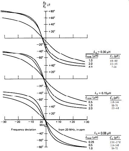
Figure 7.20. Phase shift versus frequency for Butler circuits, L-tap,
3. The impedance of L, must be equal to or less than the crystal's internal series resistance R, if the crystal's load impedance is to be kept reasonably small.
4. Frequency of oscillation is relatively insensitive to the value of L,.
Making L, larger moves the oscillation band slowly downward and farther away from series resonance.
5. Slopes of the better curves of phase shift versus frequency are reasonably high, indicating that good short-term frequency stability can be had by selecting the right component values.
Frequency deviation from 20 MHz, in ppm
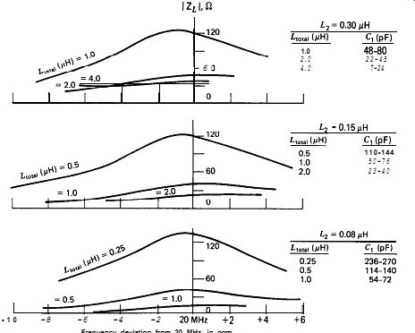
Figure 7.21. Crystal load impedance versus frequency for Butler circuits,
L-tap.
Frequency deviation from 20 MHz, in ppm
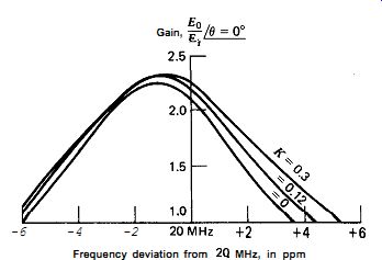
Figure 7.22. Gain versus frequency for Butler circuits, L-tap, as a function
of the coil's mutual coupling coefficient K. L1 = 0.7686 pH, L2 = 0.15 PH.
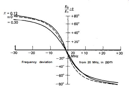
Figure 7.23. Phase shift versus frequency for Butler circuits, L-tap, as a
function of the coil's mutual coupling coefficient K. L, = 0.7686 pH, L, =
0.15 PH.
6. Maximum gain is about 2.4 peak for the Butler emitter follower circuit. And although it is not shown in the figures, maximum gain for the Butler common base circuit was calculated as 0.035 peak.
The curves in Figs. 7.19,7.20, and 7.21 were calculated the same way as curves in Figs. 7.14, 7.15, and 7.16. The reader is referred to Section 7.6 for an explanation of how these curves were calculated.
All six of the analytical results have been observed experimentally in test circuits, with one important difference. The inductive tap circuit would oscillate only below and not at series resonance. In the test circuits, gain curves in Fig. 7.19 appeared to be shifted about 5 ppm farther down in frequency. The Butler emitter follower circuit (but not the Butler common base circuit) could be made to oscillate at series resonance or slightly above it, just as Fig. 7.19 shows, by removing the diode amplitude clamp across the coil. Why this happens is not understood.
Frequency deviation from 20 MHz. in ppm
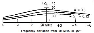
Figure 7.24. Crystal load impedance versus frequency for Butler circuits,
L-tap, as a function of the coil's mutual coupling coefficient K. L, = 0.7686
pH, L, = 0.15 /AH.
The inductive tap circuit differs from the capacitive tap circuit in that it has mutual coupling between the two tapped portions of the coil. Does the mutual coupling have any effect on the circuit? Not much, it turns out. The maximum practical value of the coefficient of coupling K for a single-layer tapped solenoid is about 0.3. Figures 7.22, 7.23, and 7.24 show calculated values of circuit gain, phase shift with frequency, and crystal load impedance for three values of K (0, 0.12, and O-30), while leaving the values of L, and L2 constant. As can be seen from the curves, the slope of the circuit's phase shift with frequency, the gain, and frequency of oscillation change very little when K changes. Only the crystal's load impedance changes significantly, increasing about 50% over the full range of K from 0 to 0.3.
The effect of mutual inductance on the circuit was checked in test circuits by breaking the tapped coil into two separate inductors oriented at 90 degr. for minimum coupling (K = 0). The peak of the oscillation band did not shift, staying at about 5 ppm below series resonance, and the oscillation frequency stayed below series resonance.