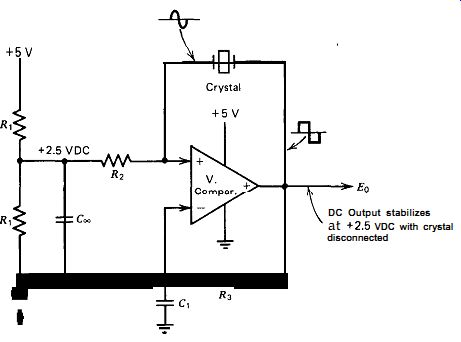
Figure 9.1. Solving the start-up problem with negative feedback.
| Home | Audio mag. | Stereo Review mag. | High Fidelity mag. | AE/AA mag. |
Normally, when power is applied to an oscillator, we expect it to start oscillating. Unfortunately, it does not always start unless positive steps are taken to make sure it does. The key is DC biasing, and the solution is a little different for discrete transistors than for integrated circuits. The first section of this section covers biasing ICs, while the second covers biasing discrete transistors.
9.1. BIASING ICs
The amplifiers used in most of the IC oscillator circuits in this guide are digital amplifiers: logic inverters, line receivers, voltage comparators, and so forth. They are designed to be used in either a "0" or "1" state. In either state, the amplifier is saturated, and the gain is zero. For oscillation to occur, a circuit's loop gain must be greater than one. Once oscillation starts, energy storage in the crystal will carry the oscillator through the saturated zero-gain intervals. Loop gain exceeds one only during switching intervals between binary states, closing the loop over part of each cycle. When power is first applied to a digital circuit, however, there is no energy storage in the crystal. And if the amplifier is in either binary state, loop gain is zero, and oscillation will not start.
The key to the start-up problem is selecting digital amplifiers to which negative feedback can be applied, in order to bias the amplifier's input and output terminals in the middle of their transition zones between the zero and one states, where the digital amplifier has a finite gain. Since negative feedback is needed only for DC biasing conditions, a shunt capacitance to ground can be added after the feedback resistor to (1) provide a 6-dB/octave frequency roll-off that will ensure a stable feedback amplifier condition and (2) limit the gain-reducing effects of the negative feedback network to low frequencies. The negative feedback network ensures that oscillation will always start when power is applied.
For an example, refer to the oscillator circuit in Fig. 9.1. This oscillator uses a voltage comparator as an amplifier. The voltage comparator is assumed to be a TTL unit with an output swing between 0 V and +5 VDC.
The midpoint of the two resistors R, and R, provides a +2.5 VDC reference point halfway between binary zero and one output states. The positive (+) amplifier input terminal is tied to this DC reference point by R,, and the comparator output will tend to follow this input toward one or the other of its two binary states. R, provides negative feedback from the amplifier output to the negative (-) input terminal of the amplifier in order to force the output voltage to follow the input voltage, and it stabilizes at +2.5 VDC. Capacitor C, limits negative feedback to low frequencies and together with R,, provides a 6-dB/octave roll-off, which gives an inherently stable feedback amplifier condition. Both amplifier input and output are then in an unsaturated state, being biased in the middle of the transition zone, and the gain through the comparator amplifier is then greater than zero. All IC oscillators in this guide use the negative feedback concept to ensure oscillation at start-up.
Figure 9.1. Solving the start-up problem with negative feedback.
9.2. BIASING DISCRETE TRANSISTORS
Just as with an IC oscillator, a discrete transistor oscillator must be biased within its linear region if it is to start oscillating when power is applied. It is preferable to bias the transistor stage near the middle of its linear region, which means adjusting the bias so that the collector's DC output voltage is held halfway between ground and the power supply voltage. Figure 9.2 shows an assortment of DC biasing methods for a common emitter pulse-amplifier stage. These biasing circuits illustrate the tradeoff between circuit complexity and bias stability. The first three use a passive biasing arrangement, the second three use an active constant-current arrangement, and the last one uses an active voltage feedback circuit. A short description of each configuration follows.
The simplest biasing arrangement is shown in Fig. 9.2a and is useful only at low and medium frequencies in a benign environment. There is no correction in this circuit for gain changes with temperature, and an adjustable resistor R, is required to handle gain differences between individual transistors. The collector's output voltage changes considerably if the power supply voltage changes by even a small amount. The circuit does not work well at high frequencies because it does not have a base to-emitter discharge resistor R,, as shown in Fig. 9.2b. This resistor R, is required for fast discharge of the transistor's base-to-emitter junction capacitance.
Figure 9.2b shows a biasing method that works a little better. Negative DC feedback from the collector is used to bias the transistor's base.
Depending on the value of R,, negative feedback will hold the collector's output voltage somewhere between a constant voltage and half the supply voltage, over a reasonably large supply-voltage change. Gain changes with temperature are partially corrected for. An adjustable biasing resistor R, is required to handle gain differences between individual transistors. This circuit will work at high frequencies because it has a base-to-emitter resistor R, for fast discharging of the transistor's base-to-emitter capacitance.
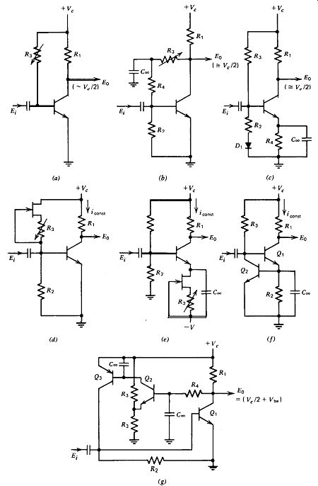
Figure 9.2(a-g). Some DC biasing schemes for a common emitter pulse amplifier
stage.
The biasing arrangement shown in Fig. 9.2c is widely used because it does not require an adjustable resistor. The collector's output voltage holds reasonably close to half the power supply voltage, with large changes in the power supply voltage and gain changes with temperature reasonably well-corrected for. The key to biasing this circuit is holding the base at a constant bias voltage (with a fixed power supply voltage) over the three to one differences in emitter current between individual transistors. An emitter resistor R, is required and used as an emitter cur-rent feedback resistor. R, is selected to be a reasonably large percentage of the collector resistor R,. The biasing resistors R, and R, are given medium resistance values, so that the usual 3 to 1 variation in the base biasing current between individual transistors does not shift the base biasing voltage significantly. Diode D, compensates for the transistor's base-to-emitter voltage drop. The diode is sometimes omitted in order to reduce circuit complexity. A fair amount of calculation is required to design this circuit, using maximum and minimum transistor gains and gain changes with temperature.
Figure 9.2d uses a FET to provide constant biasing current into the transistor's base. Depending on the value of R,, the collector's output voltage is held somewhere between a constant voltage and a fixed voltage increment below the power supply voltage. Gain changes with temperature are not corrected for. An adjustable biasing resistor R, is required to compensate for pinch-off voltage differences between individual FETs and gain differences between individual transistors.
Figure 9.2e is useful if a negative supply voltage is available. It operates the same as Fig. 9.2d except that gain differences between individual transistors and transistor gain changes with temperature are corrected for. FET gain changes with temperature can be compensated for by adjusting current through the FET to its temperature null value. An adjustable biasing resistor R, is required to handle pinch-off voltage variations between individual FETs.
Figure 9.2f uses an emitter resistor R, to sample the emitter current of Q1, Q2 varies bias voltage on Q r to maintain a constant emitter current in Q,. Q,'s collector output voltage is maintained at a fixed voltage increment below the power supply voltage. Gain changes with temperature are partially compensated for.
The best biasing scheme is also the most complex one, and it is shown in Fig. 9.2g. Figure 9.2g uses two transistors in a voltage-feedback scheme from the collector to the base of Ql. It maintains the collector of Q1 at one-half the supply voltage plus one Vi,, (base to emitter voltage, about 0.4 V). Transistor Q2 measures the voltage difference between the collector of Qr and the center point of the two resistors R, and R,, which is amplified and fed back to the base of Qr. Q,'s collector voltage holds quite accurately at half the supply voltage plus one Vbe because of the gain in the feedback loop. Gain changes with temperature in all of the transistors are corrected for, and no adjustable resistor is required.