RF amplification
The signal that is read from the compact disc and contains the data information is the RF signal, that consists of the sum of signals (A + B + C + D) from the main spot detector. At this stage, the signal is a weak current signal and requires current-to-voltage conversion, amplification and waveform shaping. The CDP-101 RF amplifier circuit is shown in FIG. 1. IC402 is a current to-voltage converter and amplifier stage, while IC403 is an offset amplifier, correcting the offset voltage of the RF signal and delivering the amplified RF signal.
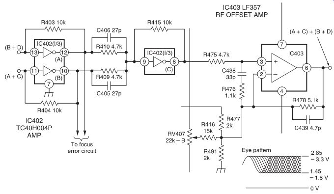
FIG. 1 RF amplification circuit of the CDP-101 compact disc player.
FIG. 2 shows the waveshaper circuit used in the CDP-101.
Because the RF signal from the RF amplifier is a heterogeneous signal due to disc irregularities, the waveshaper circuit detects correct zero-cross points of the eye pattern and transforms the signal into a square wave signal. After waveshaping by IC404, the signal is integrated in the feedback loop through a low-pass filter circuit to obtain a DC voltage applied to the input, so as to obtain correct slicing of the eye pattern signal.
FIG. 3 shows a timing diagram of the RF signal before and after waveform shaping.
Signal decoding
The block diagram in FIG. 4 represents the basic circuit blocks of a compact disc player. After waveshaping, the RF signal is applied to a phase-locked loop (PLL) circuit in order to detect the clock information from the signal which, in turn, synchronizes the data.
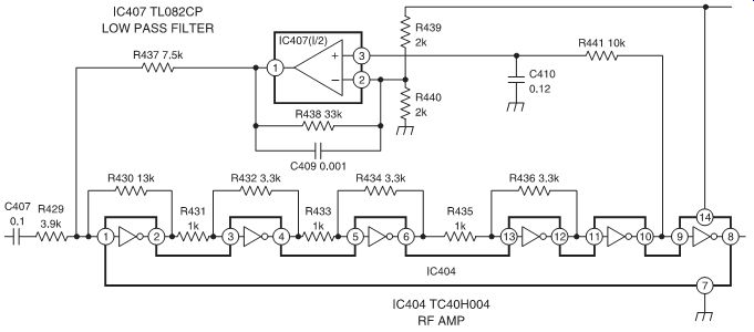
FIG. 2 Waveshaping circuit used in the CDP-101.
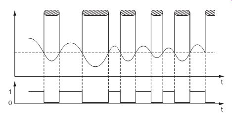
FIG. 3 Timing diagram of the RF signal before and after waveshaping.
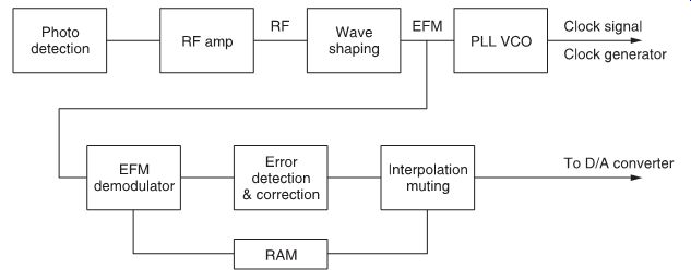
FIG. 4 Signal decoding within the compact disc player.
Also, the RF signal is applied to an EFM demodulator and associated error stages in order to obtain a demodulated signal. In the CDP-101, a single integrated circuit, the CX7933, performs EFM demodulation; a block diagram is shown in FIG. 5.
This block diagram shows frame sync detection, fourteen-to-eight demodulation to a parallel 8-bit data output, subcode Q detection and generation by an internal counter and timing generator of the WFCK (write frame clock) and WRFQ (write request) synchronization signals. FIG. 6 shows the EFM decoding algorithm (for comparison with the encoding scheme in Figure 9.2).
CIRC decoding is performed by a single integrated circuit, the CX7935 (FIG. 7), on the data stored in the RAM memory.
An RAM control IC, the CX7934 (FIG. 8), is used to control data manipulations between the RAM and the rest of the demodulation stage circuits.
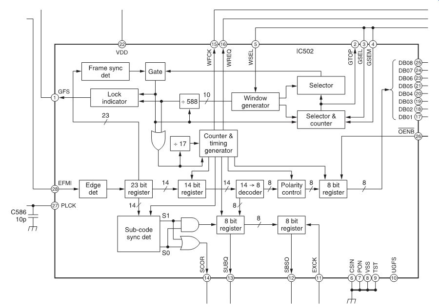
FIG. 5 Block diagram of the CX7933 integrated circuit, which performs
EFM demodulation in the CDP-101.
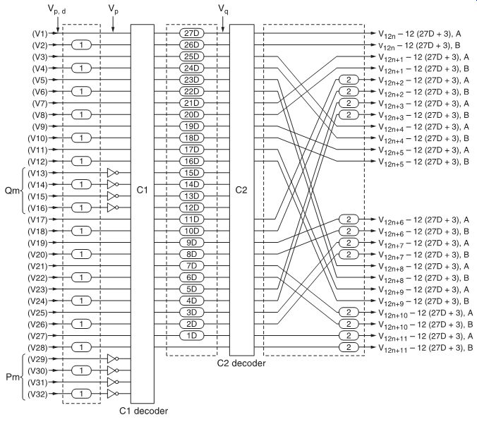
FIG. 6 CIRC decoding algorithm.
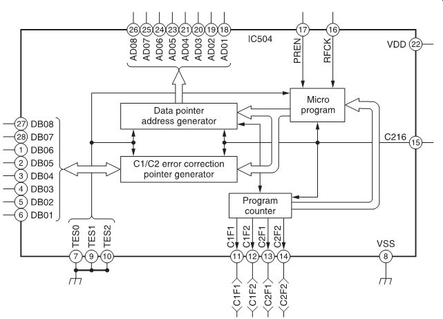
FIG. 7 Block diagram of the CX7935 CIRC decoder.
The data are checked, corrected if necessary and de-interleaved during read-out. If non-correctable errors are found, a pointer for this data word is stored in memory and the circuit corrects the data by interpolation. FIG. 9 shows the complete signal decoding circuit as used in the CDP-101. In the latest Sony CD players, signal decoding is performed by a single integrated circuit, the CX23035, shown in FIG. 10.
D/A converter
The D/A converter follows the signal processing and decoding circuits. FIG. 11 represents the CX20017 integrated circuit D/A converter as used in Sony CD players. The converter is formed around an integrating dual-slope A/D converter. Two counters, one for the eight most significant and one for the eight least significant bits, control the two constant-current sources (which have a ratio: Io /i o = 256) used for charging the integrator capacitor. Conversion is controlled by the LRCK (left/right clock), BCLK (bit clock) and WCLK (word clock) signals.
FIG. 12 represents the operating principle, where 16-bit data are loaded into the two 8-bit counters by a latch signal. With data in the counters, no carry signals exist and the current switches are closed. The integration capacitor C charges with a total current I = I1 + I2.
During conversion, each counter counts down to zero, where upon the carry signals open the current switches, stopping further charging of the capacitor. The final charge across the capacitor, as an analog voltage, represents the 16-bit input.
FIG. 13 shows a practical application of a D/A converter circuit in a CD player.
High-accuracy D/A conversion
18-Bit digital filter/eight times oversampling
The CXD-1144 is a digital filter allowing the conversion of 16-bit samples into 18-bit samples with very high precision (FIG. 14). The remaining ripple in the audible range is reduced to ±0.00001 dB. The attenuation is 120 dB and the echo rejection is about 124 dB. In particular, the reproduction of pulse-shaped tones, such as those of a keyboard or piano, is remarkably improved by enhancing the rising edges of the signal and the high echo rejection.
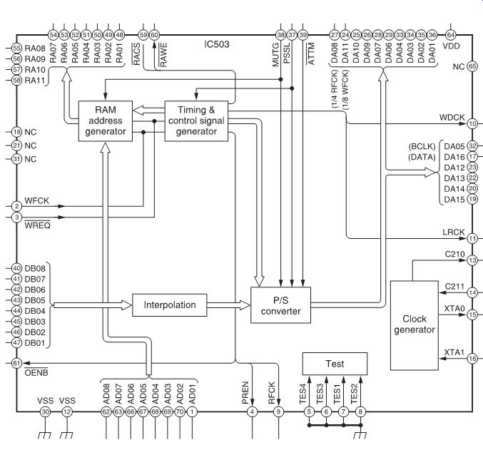
FIG. 8 Block diagram of the CX7934 RAM controller.
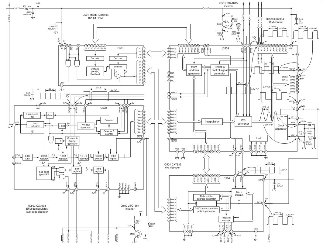
FIG. 9 Complete signal decoding circuit of the CDP-101.
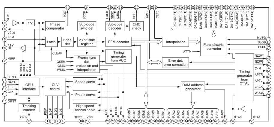
FIG. 10 Block diagram of the CX23035 integrated circuit, which performs
all signal decoding within the latest Sony CD players.
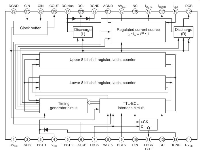
FIG. 11 Block diagram of the CX20017 D/A converter.
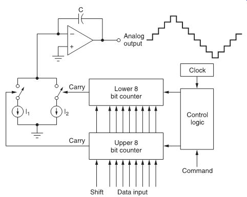
FIG. 12 Operating principle of the CX20017 D/A converter.
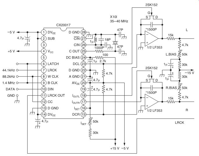
FIG. 13
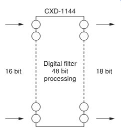
FIG. 14 CXD-1144 digital filter.
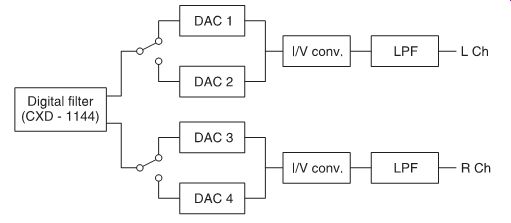
FIG. 15 Overlapped staggered D/A conversion system.
The digital filter is also used to create oversampling, calculating the intermediate values of the samples. An oversampling of 8 f s or 352.8 kHz can be achieved. This increase in sampling rate gives an important reduction of quantization noise, which allows a more pure and analytical playback of music. Also, a lower order LPF can be used, improving the group delay and linearity in the audio range.
In order to cope with 18-bit and such a high conversion rate, great care must be taken in the designing of the D/A converter.
To reduce the load imposed on the D/A converter, Sony developed an 'overlapped staggered D/A conversion system' (FIG. 15). The basic idea is to use a digital filter circuit at 8 f s output, combined with two D/A converters for each channel.
The conversion rate is 4 f s , so the digital filter output is at 2 × 4 = 8 f s oversampling. The even and odd samples for each channel are applied to separate D/A converters. By adding the output of both D/A converters, corresponding to the formula (L1 + L2 )/2, a staircase signal is obtained which corresponds to an 8 f s over sampled output signal. Since the outputs of the two D/A converters are added continuously, a maximum improvement of 3 dB is realized in quantization noise with reduced distortion.
The output current is also doubled, improving the signal-to-noise ratio of the analog noise by a maximum of 6 dB.
High-density linear converter
FIG. 16 shows a block diagram of a single-bit pulse D/A converter. The digital filter, CXD-1244, uses an internal 45-bit accumulator to perform accurate oversampling needed in the single-bit converter. The pulse D/A converter combines a third order noise shaper and a Pulse Length Modulation (PLM) converter to produce a train of pulses at its output. By using a low-order LPF, the analog signal is obtained. A digital sync circuit is inserted between the D/A converter and the digital filter to prevent jitter of the digital signal.
Compared with conventional D/A converters, the high-density linear converter provides highly accurate D/A conversion with improved dynamic range and extremely low harmonic distortion.
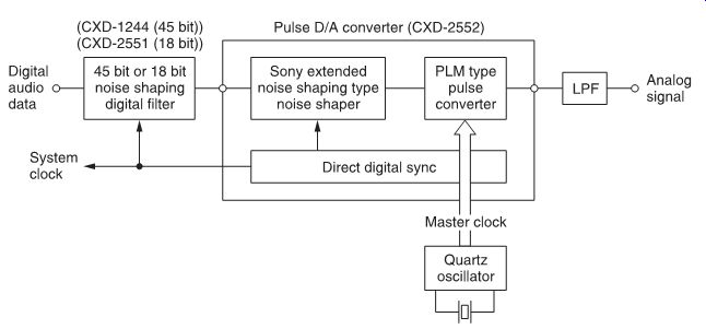
FIG. 16 Single-bit pulse D/A converter.