047 4-WAY DAC EXTENSION
This extension circuit makes it possible to use a single DAC (digital-analog converter) for generating four analog voltages. Evidently, the cost of the extension described here is only a fraction of that of four DAC chips.
The operation of the 4-way DAC is fairly simple.
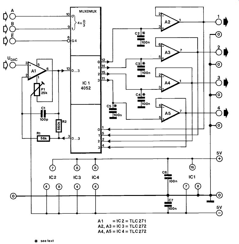
Assuming that inputs A, B and E of multiplexer/demultiplexer IC, are driven low, the output of A1 is fed to the + input of A2, while the output of this opamp is connected to the- input of A1 via the demultiplexer and R1. Capacitor C2 functions as a storage device. The output voltage available at terminal 1 equals UDAC because A1 is dimensioned for unity gain. When the E input is driven high, or when a new code is applied to inputs A-B, the input voltage for A2 is derived from C2 , so that the programmed voltage remains available at the output. The function of the other output buffers and capacitors is, of course, similar to that of A2-C2 .

------------
For optimum performance, C2-C5 should be low leakage capacitors, e.g. multilayer MKT, and the input current to A2-A5 should remain low. The latter condition is satisfied by using opamps with FET inputs (typical bias current: 1 pA). Only A1 requires an offset compensation since feed back is provided via the lower multiplexer in IC1. The E (enable) input serves to disable IC1 during switchover to another channel. R2 then gives A, unity gain to prevent the input being left open.
When a Type HCT4052 is used in the IC, position, standard TTL levels can be used to drive inputs A, B and E.
A "normal" CMOS 4052 requires 5K6 pull-up resistors to be fitted on these inputs, but only if TTL signals are used to drive the extension. The current consumption of the circuit is less than 10 mA. UDAC should be between -3.5 V and + 3.5 V.
048 8-BIT ADC
Before any analog voltage can be measured and subsequently processed by a computer, a converter device with the necessary precision is required to provide the computer with the digital n-bit equivalent of the voltage as applied to the DAC circuit.
Obviously, the higher n, the more steps involved in the conversion process, but also the higher the accuracy that can be obtained.
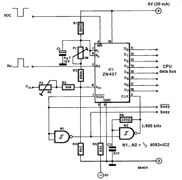
This 8-bit ADC circuit works with very few parts; yet it is versatile, fast, and sufficiently accurate for most purposes. The maximum input voltage to the circuit is arranged at 5V, as determined by the resistor network connected to the A_in terminal of the Type ZN427 ADC chip. Given this upper limit for Vin, the conversion accuracy equals 5V/(28-1) = 19.6mV/step. Other input voltage levels may be accommodated by appropriate re-dimensioning of the input voltage divider.

-----
Since the proposed ADC chip features an analog-to-digital conversion time of only 10µs (typical value), alternating voltages may be measured (digitalized) and processed under machine language control; just as with the above DAC circuit, BASIC is usually not very suitable for this purpose, and its use is restricted to applications where timing requirements are less stringent. It will be understood that fast and therefore smooth computer response to, say, joystick movement is only feasible if the ADC reading subroutine is written in machine code.
A low SOC (start of conversion) pulse at the WR in put of the chip triggers the internal voltage conversion process and the BUSY output is activated (i.e. pulled low); this, in turn, enables Schmitt trigger gate Ni to generate the ADC clock frequency of about 900kHz. On completion of the clock-controlled conversion, BUSY goes high, and the CPU may read the 8-bit value contained in the ADC latch by activating the read line. Note that the SOC and read signals must be decoded with suitable circuitry as required by the type of computer or CPU. Provision has been made in the ADC circuit to select either the BUSY or BUSY signal in order to flag the conversion condition to the host computer CPU.
Calibration of the present circuit is straightforward, since this merely involves setting two presets. First, a simple test loop may be written in machine language; next, adjust P1 (offset) for a computer reading of 0 with no input voltage applied to the circuit; P2 is set to give a reading of 255 (FFhex) with the maximum input voltage at Vin, i.e. 5V. Finally, test the ADC linearity by applying 2.5V from a sufficiently accurate source; the computer should read 128 (80 hex).
049 8-BIT DAC
---------- This simple circuit enables computer users to generate analog voltages under software control, which, no doubt, offers interesting possibilities for intelligent control of, for example, volume adjustment of audio equipment, light dimmer circuits, etc.
It is also possible to write machine language algorithms for the generation of several different, complex periodic output voltages, in short, to con struct a computer-controlled function generator using a minimum amount of hardware.
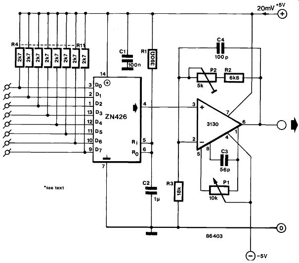
The circuit is based on the Type ZN426 digital-to-analog converter (DAC), which is an 8-bit resolution (255-step), high conversion speed (1 pts) device for direct microprocessor interfacing. The circuit may be connected to an 8-bit output port which provides TTL or CMOS compatible digital levels; most computers currently on the market have such a port, or the manufacturer has made provision to add one or more of these in the form of an expansion. The conversion time of the DAC chip allows the use of machine code for high frequency output voltages; BASIC is usually too slow for this purpose.
The DAC output voltage is buffered with an BI-FET opamp, which can be adjusted for a step response of 15mV/step, which means that the maximum output voltage of the present circuit is 3.825V, since 8 bits represent 255 steps (28-1).
Adjustment of the circuit is straightforward: connect a DVM to the output and adjust P1 for an indication of 0.00V with zero (0) written to the DAC; next, write 255 (FFhex) and adjust P2 for the maximum voltage indication of 3.825V.
The circuit is also very suitable as an D-to-A converter driven by 8-bit I/O port (EE, December 1985) as part of the universal I/O bus. It should be noted, however, that writing FF hex to this port gives an analog output voltage of OV, since the ULN2003 buffer IC in the 8-bit output port is an inverting device: moreover, the eight data lines to the DAC chip should be fitted with pull-up resistors as shown in the circuit diagram.
050 16-KEY INPUT FOR MSX MICROS
This simple circuit is an unusual, but interesting, application of the joystick port available on an MSX microcomputer. With some modifications, it should also work with other types of computer equipped with a similar "game" input. The use of the joystick port for reading 16 switches is advantageous because very little additional hardware is required, and programmers can avail themselves of standard BASIC instructions relating to the joystick.
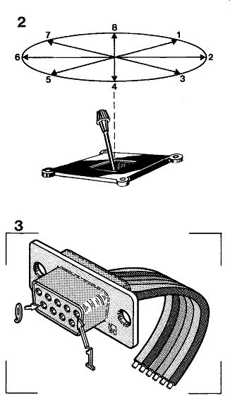
On MSX computers, the position of the joystick handle is read with the aid of instruction STICK (n), where n is 1 or 2, i.e., the number of the relevant joystick. The instruction returns an integer between 1 and 8, from which the handle position is deduced as shown in Fig. 1. Instruction STRIG(n) enables determining the state of the trigger (fire) button on joystick n, and returns -1 when this is actuated.
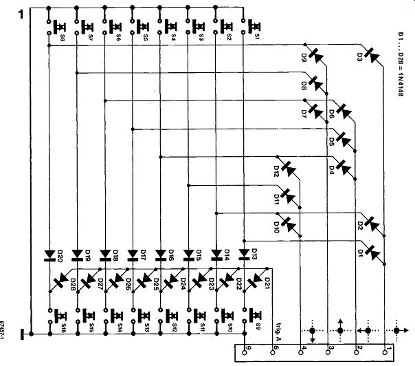
A diode matrix is used here to enable connecting eight pushbuttons S1-S8 to the four direction inputs on the joystick port. When actuated, either one of these buttons forces a logic low level upon one or two of the input lines, enabling the computer to identify the key number. Eight additional diodes, D21-D28, make it possible to double the number of keys (S9-S16). These can be kept distinct from the former 8 by connecting them to the trig. A input.
The 16 keys are identified in BASIC with the aid of instructions X = STICK (1) (or X = STICK (2)) and Y = STRIG (1) (or Y = STRIG (2)) so that the key number is simply Z = X-(Y*8) + 1.
This goes to show how a versatile extension can make good use of existing hardware whilst being controllable with BASIC commands. Finally, Fig. 3 shows the pin assignment on the 9-way sub D connector used for connecting the present circuit to the MSX joystick port.
-----------
051 32 KBYTE PSEUDO-ROM
This versatile, exchangeable, memory module should appeal to programmers developing software for computers other than the one being used for writing, testing and debugging the program. The battery back-up function of the module ensures that data is retained, and so makes it possible to use "portable", software that is ROM-based and yet can be altered readily without having to program and erase an EPROM a number of times.
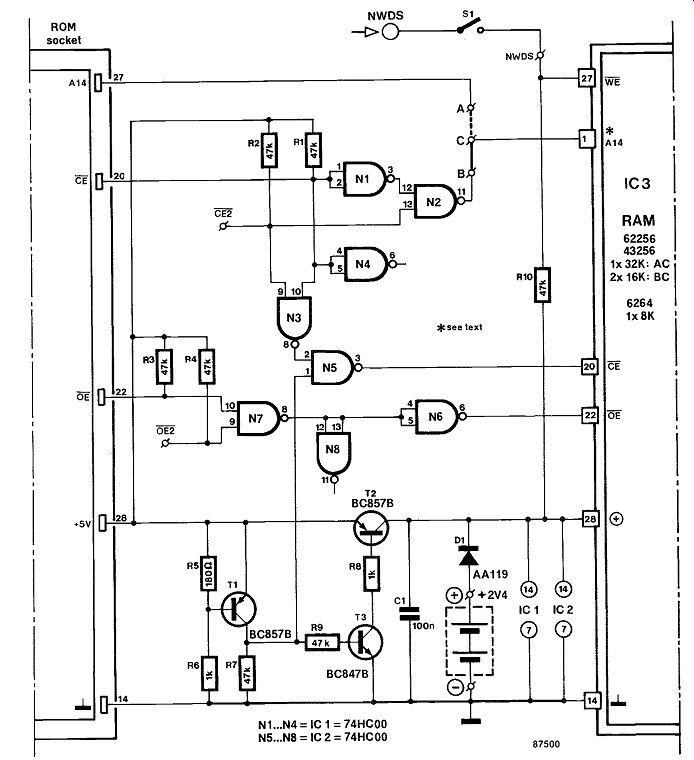
The memory module is based on the use of a Type 43256 32 Kbyte static CMOS RAM from NEC see Fig. 1. Other 32 K types, such as the 62256, should also work here. A battery (2 button cells, or a 2.4 V NiCd cell when D1 is bypassed with a resistor to enable charging) enables the chip to retain its contents when the computer is off. When the + 5 V supply from the computer is on, T1 drives pin 1 of Ns high, so that this gate can enable the RAM via the CE input. The supply set up around T3-T2 then feeds all the chips on the board with about 4.8 V. The drop across the C-E junction of T2 is less than 0.2 V here since the transistor is driven into saturation. When the computer is switched off, the circuit is fed from the battery via germanium diode D1. Voltage divider R6-R6 causes T1 to be turned off when the supply level drops below some 4.5 V.
Input I of N5 is grounded via R7, so that CE on the RAM is held high, causing the chip to switch to the power-down (standby) mode. A prototype of the plug-in RAM consumed only 1.5 µA in the data retention mode, after briefly taking about 3 mA when the input voltage dropped from 1.5 to 1V.
This effect is normal, however, and is due to the in puts of the HC gates briefly being in an undefined state. The ICs fitted were Types 74HC00 (SMD) and a 43256C-12L (120 ns).
---------
The module is configured as a 32 Kbyte RAM block by fitting wire jumper A-C, while jumper B-C selects 2 x 16 Kbyte. The latter configuration is required when the socket that receives the module is intended for a maximum memory capacity of 16 Kbyte (ROM or RAM), as on the BBC sideway extension board. A Type 6264 RAM can be used in the IC3 position when only 8 Kbytes are required.
Neither jumper need then be fitted.
Successfully constructing the RAM module re quires great care in soldering the SMA parts onto the board shown in Fig. 2. It is absolutely necessary to first fit all the SMA parts at both sides of the board, then the three wire links and jumper B-C or A-C as required. Do not forget to solder the terminals of D1 (not an SMA part), and the battery connections, at both sides of the board. Also, through-contacting with short lengths of component wire should be effected at four locations. Push all the pins of two 14-way IC terminal strips through the straight rows of holes on the component side of the board, i.e. the side that holds the transistors, then solder the pins to the islands on the copper side, i.e., the side that holds the 74HC00s.
The pins should protrude at least 4 mm. The use of a centrally cut wire-wrapping socket is not recommended here in view of the thickness of the pins.
Locate the pin that protrudes from the hole marked 1, and cut it off. Mount a turned IC pin holder next to pin 28, 27, 22 and 20 of the right-hand side terminal strip, and solder these at both sides of the PCB. These pins should not protrude at the copper side, and their tops should be 1.5 to 2 mm above those in the terminal strip. When it is intended to use the RAM in its 2 x 16 Kbyte configuration, wires are connected to points 0E2 and CE2 at the copper side, and guided between pins 5-6 and 9-10 respectively. Remove pin 1 of a standard 28-way IC socket, before carefully push-fitting this onto the 27 protruding pins at the copper side. Connect the battery supply wires and the wire to S1 (NWDS) to the respective points at the component side. Use a pair of precision pliers to carefully bend pins 28, 27, 22 and 20 of the 43256 or 6264 slightly to the right of the other pins in the row. This enables pushing these four IC pins in the previously mentioned, separate, socket pins, while the 24 others are inserted in the usual manner. The battery is conveniently mounted at some distance from the module. When a miniature battery is available, this can be fitted underneath the RAM chip. For BBC users: wires 0E2 and CE2 are conveniently connected to pins 22 and 20 respectively of a 28-way IC socket for plugging into the adjacent ROM/RAM socket on the BBC's sideway extension board; the NWDS signal is available at pin 8 of IC77. Switch S1 is mounted at a convenient location on the computer's rear panel, and when opened inhibits writing into the RAM. It is recommended to open S1 after turning the computer off to prevent the battery having to supply some 50 µA for prolonged periods: this current flows into the NWDS driver via Rio. Non-BBC or Electron Plus-1 users should note that the NWDS signal is the same as WRITE, not READ/WRITE.
The MOVE command in the ADT ROM available for the BBC computer enables exchanging data between resident and sideway memory. Programmers should have little difficulty, however, in writing a short routine that selects the relevant sideway socket(s) via the socket latch at FE3Ffi, and copying one or two 16 Kbyte blocks.
Parts list
Note: all parts Surface Mount Assembly types unless marked Resistors:
R1 ... R4 incl.; Ri;139; R10 =47K Rs= 180R R6; R8= 1K0
Capacitor:
C1 =100n or 47n Semiconductors:
D1=AA119
T1;T2=BC857B or similar pnp SMA type.
T3 = BC847B or similar npn SMA type.
IC1;IC2=74HC00 (Do not use HCT types).
IC3=43256C-10/12/15L (NEC) or 62256 LP10/12 32Kbyte CMOS static RAM.
Miscellaneous:
PCB Type 87500 2 off 14-way terminal strips with 7 mm pins.
4 off turned pins for IC leads.
Suitable battery (see text, V b 2.4 V)

052 40-TRACK ADAPTOR
Over the past few years, the cost of 5 1/4 inch floppy disk drives has gone down to the extent that modern, 80-track, double-sided drives now cost less than a simple, 40-track, single-sided type some three years ago. It is, therefore, not surprising to see many computer owners upgrade their systems with a set of 80-track, slim-line drives to boost the mass storage capacity of their micro.
However, 40-track stored programs are not readily retrievable in the new system, because the distance between tracks in the 40-track drive is twice that in the 80-track model.
This circuit offers a solution to the problem, in that 80-track disk drive, so as to make it "look like" a 40 track type to the computer which should, of course, be programmed with a 40-track disk operating system (DOS).
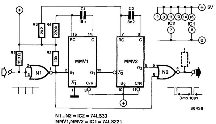
It is seen from the circuit diagram that Gate Ni receives the FDC controller STEP pulse, which is used in the circuit as a timing reference for the automatic generation of another STEP pulse to follow the first after 3 ms.
It should be noted that, when incorporating the circuit in an 80-track drive, the track-to-track access time in the 40-track mode is double that as given in the drive specifications, which refer to 80-track use.
---
053 2708 ALTERNATIVES
Thanks to the development of an ever expanding range of capacious EPROMs in the 27xxx and 25xxx series, the Type 2708 has become completely obsolete. Not only is this forerunner in EPROM technology relatively hard to program, it is also expensive in view of its modest 1 Kbyte holding capacity.
It stands to reason that replacement of the 2708 with either the 2716 (2 Kbytes) or the 2732 (4 Kbytes) is most readily accomplished if the differences in pin functions are first taken into consideration.
The pinning overview and associated table go to show quite conclusively that the replacement is no daunting task, since the former positive and negative supply pins to the 2708, 19 and 21 respectively, may be hard wired as suggested for either the 2716 or 2732.
It should be noted that pin 18 (CE for the 2716 as well as the 2732) is tied to ground, while pin 20 (OE) is driven by the computer CS signal. This new arrangement is of no consequence for neither EPROM nor computer, since OE may function as CE if it is realized that the EPROM can not be switched to its low power standby state anymore.
However, this minor drawback merely causes an increase in current consumption, whilst at the same time offering a faster EPROM access time, as only the three-state bus drivers are enabled internally, rather than the entire chip logic.
As the Type 2716 and 2732 EPROMs offer double and four times the capacity of a 2708, respectively, a manual address block selection may be added to the circuit; this set-up, composed of a switch and resistor (to be constructed double for the 2732) is marked with an asterisk in the accompanying diagram. Wire Ai() (and All, if applicable) to ground if you intend to stick to the 1 Kbyte EPROM contents, located in the first 1024 bytes block.

------------
054 6502 TRACER
A program that has been written into an assembler will rarely run error free on the first run. It often exhibits blurbs and other ramblings: in bad cases, there is a complete hang up and it is then necessary to start the computer afresh with a RESET.
To find such faults in a relatively easy manner, the tracer described here will be found very useful.
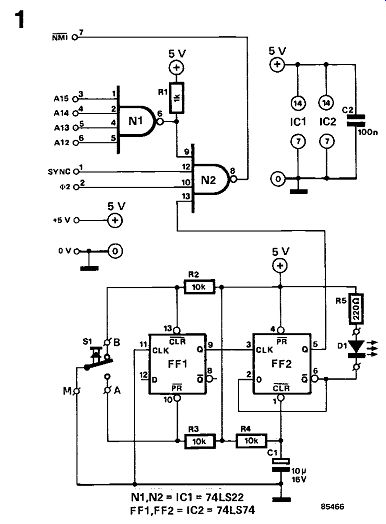
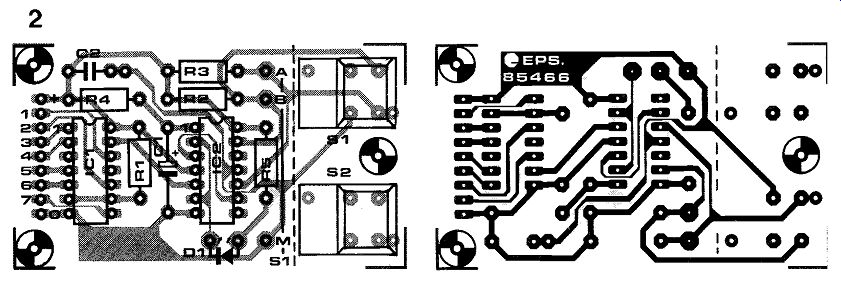
The circuit layout of the tracer is shown in figure 1.
Gate N, is an address decoder, whose output in the address range $F000. . . $FFFF is logic 0. NAND gate N2 is fed with the SYNC signal from the computer and the 0 signal; it is disabled by either the ad dress decoder, Ni, or bistable FF2. The address decoder disables N2 when the EPROM is addressed from the CPU. This prevents the SYNC line of the 6502 processor generating an MI (maskable interrupt). If the processor passes through a machine program somewhere in the RAM, N2 generates an interrupt as soon as the processor reads an opcode, which makes the SYNC line logic 1. This non maskable interrupt directs the processor to an interrupt program in the monitor program. All CPU registers are safeguarded by this interrupt program and subsequently displayed on the monitor screen.
At the same time, the processor disassembles the next command.
The programmer can, therefore, see beforehand under what conditions the processor starts with the execution of the next opcode. Since the status register and all its flags are also displayed on the screen, the programmer can easily ascertain whether a flag in the status register has been set in correctly.
Parts list:
Resistors:
R1 = 1k
R2 ... R4 = 10k
R5 = 220 ohm
Capacitors:
C1 = 10µ/16 V
C2 = 100 n
Semiconductors:
= LED (red)
IC1 = 74LS22
IC2 = 74LS74
Miscellaneous:
S1 = miniature spring-loaded press-to-make switch
S2 = miniature spring-loaded press-to-make switch (see text)
PCB 85466
Bistable FF, serves as a debounce stage; FF2 toggles on receipt of a leading edge from FF1: that is, every time S1 is pressed. When the tracer is switched on, D, lights. Resistor R4 and capacitor C1 form a power-on reset network that automatically switches the tracer off when the computer is switched on.
The printed circuit board for the tracer is shown in figure 2. If you want to build the tracer into the computer case, the PCB can be cut along the dashed line, so that the section containing S1 and S2 may be fitted in the most convenient position. Switch S1 must be connected to the tracer via a suitable cable, but S2 may be connected to the manual RESET of the system.
-----------
055 A-D CONVERTER FOR JOYSTICKS
Although joysticks come in an astounding variety of versions, their internal organization is virtually always a standard concept, based on either a set of relatively fragile, springy, membrane contacts, or two potentiometers. Many computer enthusiasts will agree that the latter, analog, type offers better reliability and quality. Unfortunately, however, these can not be used in conjunction with a popular home micro such as the Commodore C64, and that is where the present circuit comes in.
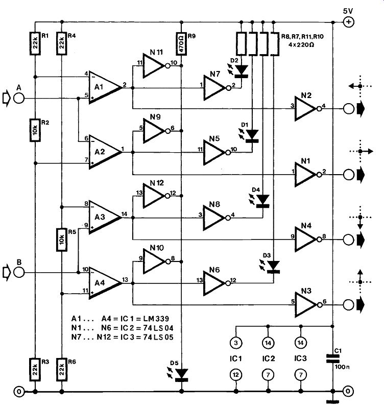
The four comparators in IC, function as switches to translate the handle movement into digital signals.
The outputs of the comparators are buffered in IC2 to enable interfacing to the computer's joystick port. The two remaining inverters in IC2, N5 and N6, along with two inverters in IC3, function as drivers for the LEDs that indicate the handle position. Gates N9-N12 are set up as a wired NOR function to enable LED D5 to light when the joystick handle is in the center position. Finally, the current consumption of the converter is about 25 mA.
-----------
056 BIDIRECTIONAL PARALLEL INTERFACE FOR C64
----
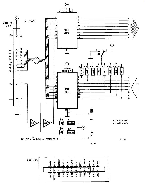
The so-called User Port on the Commodore C64 home micro is intended for connecting peripherals such as a modems, RS232 interfaces, and control circuits. In some applications, it is also used for communication with other C64s. This circuit makes it possible to use port lines PBO-PB7 as inputs and outputs. Software enables the computer to select between input and output by means of the PA2 line (terminal M).
Examples:
Data input:
10 POKE 56579,0
:REM user port is input.
20 POKE 56576,255
:REM interface is input.
30 A = PEEK(56577)
:REM read variable A.
Data output:
10 POKE 56579,255
:REM user port is output.
20 POKE 56576,251
:REM interface is output.
30 INPUT B
:REM read data-word.
40 POKE 56577,B
:REM and send to interface.
The circuit is essentially composed of 2 three-state octal bus drivers Type 8212. Via the logic level on PA2, each driver can be enabled individually so as to select between the input or output function of the interface, whose current state is indicated by a pair of LEDs. Switch S1 selects between pull-up (a) or pull-down (b) termination of the input lines.
Finally, an example for interactive data processing:
10 POKE 56567,255
:REM interface is input.
20 POKE 56579,0
:REM user port is input.
30 A = 255-PEEK(56577)
:REM read variable A.
100
:REM example of logic control:
110 IF A =1 THEN B= 64 111 IF A = 2 THEN B =128 112 IF A = 4 THEN B=192 113 IF A =1 THEN B= 32 300 POKE 56577,B
:REM load data register 310 POKE 56579,255
:REM user port is output 320 POKE 56576,251
:REM interface is output 330 GO-10 10
057 BIDIRECTIONAL SERIAL-PARALLEL CONVERTER
This interface circuit enables doing rather more than normally possible with the computer's serial (RS232) port. Serial output data from the computer is converted into parallel format, and parallel data applied to the interface is converted into a serial bit stream for reception by the computer.
The interface is based on the industry standard UART (universal asynchronous receiver/transmitter) Type AY-5-1013, or the CMOS version of it, the CDP1854 from RCA. Serial data from the computer is received at input RXD, and inverted in T1 for driving the RSI input on the UART, which converts the received word into 8-bit parallel format (RDo-RD7). The shifting in of serial bits is clocked by the 19,200 Hz signal applied to the RCP and TCP input. This fixes the baud rate of the interface at 1200 (19,200/16). The baud rate generator is a conventional design based on a binary counter/divider with built-in clock oscillator, which is crystal controlled here and operates at 2.4576 MHz. The parallel output of the UART is buffered with the aid of IC2 to enable controlling 8 relay drivers 131-138.
The parallel word applied to the UART at its TD0. TD7 inputs is converted into serial format and output via the TS0 terminal, where the signal is inverted and fed to the TXD output.
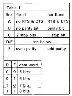
The serial data format can be defined with the aid of wire links B-F: Table 1 lists the function of each of these. Inverter T4 automatically resets the receiver in the UART by driving RDAR (received data available reset) low when RDA (received data available) goes high to signal that a complete word has been shifted into the receiver hold register.
When wire link A is installed, RDA can also control the TDS (transmitter data strobe) input, so that a new parallel word (TD0-TD7) is loaded into the transmitter holding register. Thus, jumper A makes it possible to use the CTS (clear to send) hand shaking signal. The TEOC (transmitter end of character) pulse is used here to generate the RTS handshaking signal, and also to control the TDS in put, together with CTS. This handshaking input, when active, prompts the UART to output a new serial word. Set-reset bistable N1-N2 precludes conflicts arising between the signals in question. Power on network Cl-R1 ensures that the UART is properly reset and initiated. TSO and TEOC then go high, while RDA is forced low. When link A is not fitted, the presence of the inverted TEOC pulse at input TDS causes the transmission process to commence.
Table 1

-----------
The author has developed this circuit mainly to enable two IBM PCs to communicate with the aid of the Turbo Pascal program listed in Table 2. Before this can be run, the status of serial port COM1:
(AUX:) should be defined by typing DOS command MODE COM1:1200,n,8,2 <CR>
(1200 baud, no parity, 8 data bits and 2 stop bits).
Pins 6 (DSR) and 20 (DTR) on the 25-way D socket should be interconnected, and the same goes for pins 4 (RTS) and 5 (CTS) when no handshaking is being used. When it is intended to use the hand shaking facility on the bidirectional interface, link A should be removed, and socket pins 4 and 5 connected to interface terminals CTS and RTS respectively.
058 BUS DIRECTION ADD-ON FOR MSX EXTENSIONS
The majority of MSX computers do not require a BUSDIR (bus direction) signal from add-on circuits plugged into slots. A problem arises, however, if the extension circuits published in Elektor Electronics are used in conjunction with, for example, a Sanyo MSX machine, which has a few peculiarities in its external I/O concept. In general, the more slots on an MSX computer, the higher the probability that either one of, or both, these circuits are required to be able to use the home-made extensions.
Two solutions are offered to provide for the BUSDIR signal. One is usable for the Universal I/O Bus and the I/O & Timer Cartridge, the other for the Cartridge Busboard. Each of these circuits consists of one IC only.
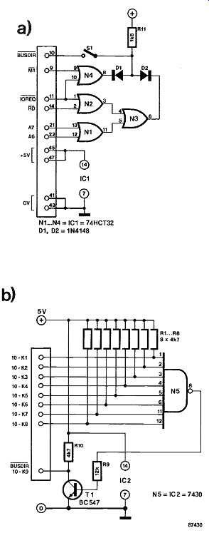
Circuit A is used with the two I/O extensions, and is readily incorporated in the computer, at a suitable location near the slot that receives the extension. If necessary, all slots on the computer are fitted with this circuit, but this makes it impossible to utilize cartridges that do supply a BUSDIR pulse, unless S1 is included to disconnect the output of N4 from slot pin 10. Note, however, that this switch must not be operated when the computer is on.
As I/O range 40h-FFh is reserved for the computer-resident hardware, address lines A6 and A7 must be low for the selection of external I/O circuitry. Moreover, IOREQ and RD must be low to ensure that BUSDIR is only active when the CPU reads data from an I/O device. Interrupts from an external device can only be processed correctly when BUSDIR is low in response to M1 and IOREQ being low also. This requires an OR function for logic low levels:
BUSDIR =MI IOREQ + IOREQ RD A7 A6
If you are hesitant about opening the computer to install circuit A, you may consider the use of a part of the EPROM cartridge board to hold the 74HCT32 as shown in the accompanying photo graph. Note that the 50-way track connector plugs straight into a computer slot, and that a slot connector is fitted at the other side of the "adaptor-PCB" to receive cartridges.
Circuit B is intended for use on the Cartridge Busboard. Its function is to pass BUSDIR pulses from cartridges to the computer. To this end, it is necessary to first break the interconnecting tracks between slot pins 10 so as to make all cartridge BUSDIR outputs separately available for wiring to 8-input NAND gate N5. Inverter T1 turns this simple add-on unit into an 8-input OR gate for logic low levels. The collector of this transistor is wired to pin 10 of Ks on the busboard.
It may well happen that both circuit A and B are required for a specific I/O arrangement. In that case, it is suggested to fit circuit A on one slot of the Cartridge Busboard, and consequently use only that slot for external I/O. Pin 8 of N4 is then connected direct to the relevant input of Ns.
Note: articles in the series MSX Extensions were published in the following issues of Elektor Electronics:
January 1986, February 1986, March 1986, January 1987, March 1987, April 1987.
----------
059 COMMUNICATION PROGRAM FOR C64
This program enables users of the popular Commodore C64 home computer to exchange messages between two machines.
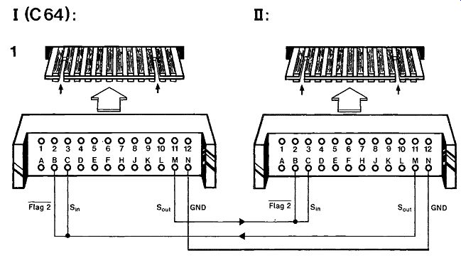
No hardware whatsoever is needed to accomplish: communication over several tens of meters using a three-wire connection--see Fig. 1. Longer distances, or communication over the telephone, of course require the use of a modem.
split screen operation: the upper half of the screen displays the operator's input (LOCAL), the lower half displays the received messages (REMOTE).
full duplex communication, i.e. transmission and reception are quasi-simultaneous processes.
The flowcharts in Fig. 2 illustrate the structure of the proposed program. TX is short for transmitter, R X for receiver. Note that screen pointer updating routines are not apparent from these diagrams.
Unfortunately, since the C64 BASIC interpreter does not allow structured programming to be carried out, the constructs shown in the flowcharts are not readily detected in the practical BASIC program listed in Fig. 3.
Keyed-in text is transmitted to the far computer after pressing the RETURN key. The BORDER color changes to warn the user when the screen is full. Typing errors can be corrected in the usual way with the aid of the INST/DEL key. A short beep is sounded to signal the receipt of a message from the REMOTE computer.
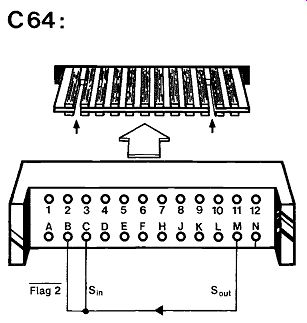
Testing the program is straightforward, and does not require two computers. Figure 4 shows the connections that can be made temporarily on the computer's user port. This creates a zero modem, and causes LOCAL text to be echoed on the REMOTE screen.
------------

------------
For those computer enthusiasts interested in analyzing the BASIC program, and for those who intend to rewrite it for other types of computer, the function of the major lines can be summarized as follows:
100-125: initialize the screen and the sound generator.
130: open the serial port with parameters 300 baud, 8 data bits, 1 stop bit, no parity, no handshaking, full duplex.
140: T is the base address of the transmit screen, and T0 is the associated index. R and R0 are similar variables for the receive screen, while R1 in addition gives the maximum number of character per line.
160: blink the cursor and read the keyboard buffer.
180-200: test for DELETE, and erase the previous character.
210-230: test for RETURN and transmit message.
240-260: toggle the BORDER color when the screen is full.
270: go to the receive subroutine.
280: repeat the above loop.
710: transmit the "begin of message" marker.
720-750: transmit and erase all characters.
Monitor the receive channel for messages, after transmission of every character; reception has the highest priority.
760: transmit the "end of message" marker.
810: blink the cursor and read the receive buffer.
820: buffer empty?
830: end of message.
840: have the sound generator produce a beep.
850-870: advance the cursor to the next line.
880: clear the new line.
900: display received character on REMOTE screen.
910-920: advance cursor to next position.
--------

-------
060 CPU GEAR–BOX
While many computer enthusiasts are keen on get ting their system to run at the highest possible clock speed, there are often quite awkward constraints posed by relatively slow, bus-connected support chips, and the ensuing frustration after failing to get reliable system operation at, say, double the 'old' clock speed may readily lead to abandoning the speed-up project altogether, for lack of precise information regarding the necessary clock-based synchronization between CPU and peripheral chip(s).
A noteworthy example of this happening in practice is the go at incorporation of the Type 9367 CRT controller in a 6502-based computer system running at 2 MHz; the specific application concerns the high-resolution graphics card published in Elektor Electronics, November 1985 ff.
This circuit ensures a correctly timed, synchronized slow-down of the system clock speed, when appropriate for CPU access to a memory-mapped (E150-El 5F) device. Following the reception of a high level on the relevant I/O line, the proposed circuit arranges for the clock signal frequency to be divided by two, while a low I/O causes division by four.
It is important to point out why the commonly used method of using 4)2 to enable the address decoder chip is to no avail when it comes to synchronous and glitch-free clock speed switching under soft ware control; the following paragraphs therefore aim at offering an insight into the basic operation of the gear-box circuit and its incorporation in a 6502-plus-graphics card system.

-------
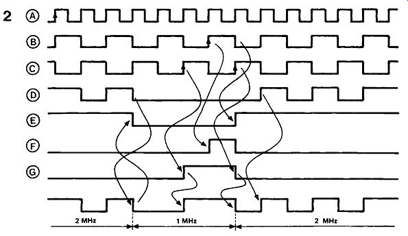
Figure 1 shows the hardware to the gear-box. A logic level at the I/O input is passed to the D (data)input of bistable FF3, as well as to the R (reset) input of FF4. FF3 toggles and activates its ohm output; this causes the 4 MHz clock signal, divided by two in FF4, to be output as 2 MHz towards the CPU 43 terminal. Division by four (1 MHz clock output) should take place in a synchronous timing arrangement as soon as I/O goes low; just prior to this pulse transition, 4).n has already gone low, so that the level change at the FF4 reset input is of no consequence to the CPU operation at that time, however the bistable can not change state anymore.
Thus, FF3 will have to supply the output clock signal; the D input follows the I/O signal transitions, since ohm of FF2 was forced to go low in con sequence of S (set) being activated. The first leading edge coming from the FF, ohm output will cause ohm of FF3 to go logic high, ending the set condition of FF2. Given an input clock frequency of 4 MHz, the outlined timing sequence results in ohm of FF2 going high after 250 ns, followed by a low level at ohm of FF3 after another 250 ns. The timing diagram shown in Fig. 2 clarifies this, admittedly rather complicated, timing arrangement in the gear box circuit. It is noted that a complete 1 MHz period has lapsed, provided FF1 is properly synchronized during the CPU initialization cycle.
Theoretical research into this matter, however, has shown that this is not always the case; the result is an asymmetrical output clock period with a logic low and high level duration of 250 and 500 ns respectively. The remedy for this undesirable effect is simple, since it merely involves interchanging the clock signal connections to FF2 and FF3.
It is seen that (ID2-based I/O decoding is less desirable, since it involves too long a delay; what re mains is to indicate the method of obtaining I/O from the graphics card system (EE, November 1985, p. 71).
XX5X is dismissed for now obvious reasons, but P = ohm at pin 19 of IC, can be used for our purpose, while the possible objections to the resultant, rather coarse address decoding are readily rendered devoid of relevance by the incorporation of a single 3-to-8 decoder Type 74LS138, mounted piggy-back onto IC2 and connected direct to pins 1. . .5, 16 and 8.
The remaining pins of the additional IC are either cut off or bent to preclude wrong contacts from being made in the circuit. However leave pins 6 and 10 in function, since the former should be tied permanently to + 5V (small wire to pin 16), while the latter can now be used to supply the correct I/O pulse for the CPU gear-box.
-------------
061 CURRENT LOOP FOR MODEM
A modem, such as the direct-coupled modem featured in the October 1984 issue of Elektor Electronics, opens a whole new world to the computer user by making possible communication between two computers anywhere in the world (provided, of course, they can be coupled to a telephone line).
Ironically, although the distance between the computers may be very large, that between computer and modem is strictly limited. This is because the RS 232 input is voltage driven and is, therefore, very susceptible to noise. This is not a new problem:
it existed many years ago when, for instance, two telex machines had to be interconnected. The solution then found, and still in use today, is the current loop. Such a current loop can also be used when the distance between the modem and the computer is relatively large: up to 1 km.
A current loop so used converts RS 232 compatible voltages into RS 232 compatible currents. The standard in the RS 232 protocol is a current loop of 20 mA.
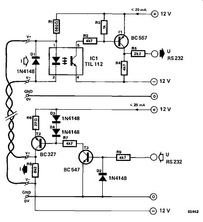
In view of the arrangement of the circuit it is possible for the current loop to be used as a voltage driven input and output. In the receiver, the opto-isolator converts the input current into an output voltage via T1. The output voltage is ± 12 V. As the current loop is closed via V + and V-, mind the polarity. If you want to use an input voltage instead of a current, apply the input between V- and earth.
The input voltage to the transmitter may vary from TTL level to ± 12 V. Its output signal is available as either a voltage or a current: the former between V+ and earth and the latter between V+ and V.
Current consumption in the quiescent state is zero; with full load, it amounts to 20 mA.
The maximum bit rate at which the circuit operates reliably is 1200 baud, but this can be increased by the use of a faster opto-isolator.

------------
062 DIRECT READING DIGITIZER
The computer to which this digitizer is coupled reads a 3-digit number that is a direct representation of the measured voltage in millivolts.
The analog-to-digital converter is an RCA type CA3162, which was designed for use in a 3-digit digital voltmeter. The input range of the IC stretches from-99 mV to 999 mV: the resolving power is, therefore, 1098 units. In other words, this converter offers a resolving power that is better than that of a standard 10-bit device for the price of an 8-bit device.
The 3-digit information at the output of the 3162 is multiplexed. The data can, for instance, be written into the micro via seven PIA (peripheral interface adapter) input lines. That means, however, that some machine language is required to be loaded into the RAM every time the converter is to be used. The present circuit uses hardware to obviate this difficulty.
The 3-digit information, which is emitted every 20 ms, is automatically loaded into three 4-bit buffers, IC8, ICs, and 1/2IC, 5, whose outputs are connected direct to the data bus. Each of these buffers has its own address. Writing the converted value into the computer has become simply a matter of reading the three memory locations, which can be carried out by PEEKs in BASIC.
The address decoder consists of IC3 ... IC5 and IC7.
The present circuit occupies a block of eight ad dresses of which only the first four are used. When the first address is read, monostable IC, is started, which causes IC, to commence the conversion pro cess. When the monostable returns to its stable state, IC, goes to the HOLD mode, and the measured voltage can be read.
An interval of not less than 50 ms is required between the start of the conversion process and the reading of the buffers.
The eight successive memory locations required for the digitizer may be placed anywhere in the memory range by means of the open inputs of gates N5.. .1\116. If any of these inputs is connected to +5 V, the relevant address line becomes logic 1; if the input is linked to 0-V, the address line goes logic low.
Assuming that the decoding has been set to address $E300, the first address is read with a PEEK, which starts the conversion.

-----------
Wait for 50 ms.
Write the data from address $E301, which is the least significant bit (LSB), i.e., the extreme right hand digit of the 3-digit number. Then write $E302 and finally $E303. At each of these transfers, an AND action must by carried out with 00001111 (binary) or 15 (decimal), because only the four lowest data bits are of import.
If the converted voltage during the further processing of the three written digits is negative, this is indicated by the data at address $E303, which is 10.
Overflow is also easily recognized: if the value read from address $E301 is 11, the voltage is greater than 999 mV; if the value is 10, there is a negative overflow.
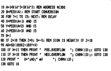
The small BASIC program given here is an example of a possible conversion routine for the Junior computer.
The circuit as shown can be used with a 6502 µ13; if it is required to be used with a Z80, RD must be connected to the R/W line via an inverter, and IORQ or MREQ is put onto the 02 line via an inverter. The choice between IORQ and MREQ depends on whether the digitizer is located in the I/O or the memory range respectively.
Take care during the construction to keep the connections marked with an asterisk (0 V and +5 V to IC)) as short as possible. These lines go together to C3 and C4, from where the connection is made to the 0 V and + 5 V lines of the digital part of the circuit. Keeping these lines short prevents possible interaction between the analog and digital parts of the circuit.
Four inputs of IC10 are not used in the present circuit, and they can, therefore, serve as four additional digital inputs. During the reading of ad dress $E303 (in the example), the highest four data bits indicate the state of these four inputs.
10 A=1616A3+3816"2; REM ADDRESS 8E300
20 IWEDUA/1 REM START CONVERSION 30 FOR T=1 TO 15: NEXT: REM DELAY 40 WEER(01) AND 15 50 Y=1,913((002) AND 15 60 b0M9(i4+8) AfiD 15 70 S=I 80 IF 2=10 THEN Z=0: S=-S: REM SIGN IS NEGATIV IF 2=10 90 AD=SX(10012+10XY+X) 100 IF X=11 THEN PRINT ' POS.OVERFLON '; CHR$(13);: GOTO 130 110 IF X=10 THEN PRINT NE6.CIVERFLCI4 '; CHR$(13);: 0010 130 120 PRINT ' U=';AD;' mV '; C/82$(13);
130 GOTO 10
063 DISCRETE DAC
------------
A digital-to-analog converter (DAC) that is easy to build from a handful of readily available parts.
The 8-bit digital input for the circuit is applied to resistors R17-R24 incl., each of which drives an associated current source composed of two series-connected diodes, a transistor and a current defining resistor fed from the positive supply rail. A logic high level at the input causes the relevant current source to be switched on, a logic low level switches it off. The sum of currents from T1-T8 incl. is arranged to pass through preset P1, which thus drops a voltage U0 in accordance with the magnitude of the 8-bit word written to the circuit.
The current supplied by each current source is about 700/R. [mA], where R. is the value of the associated resistor between the emitter and the + V rail. In order to ensure satisfactory linearity of the analog output voltage, resistors 16-Rs incl. must be dimensioned to obtain a current ratio of 1:2 between any two adjacent sources. In practice, it is wise to first apply a logic high voltage to the MSB (most significant bit) input of the circuit, leaving the remaining inputs low, and measure U0 with the aid of a good-quality voltmeter. Next, drive D6 high and all other inputs low, and make sure that U0 drops to half the previously obtained level by dimensioning R7 as required. The other current determining resistors are similarly established; the value of R1-R8 incl. that gives the correct level of U0 is obtained by making suitable combinations of series and/or parallel connected high stability resistors.
Alternatively, it is possible to use multi-turn presets.
As all resistors R1-R7 incl. must be dimensioned starting from a particular value of R8, this resistor must first be calculated considering that the output linearity of the circuit is affected unless 1.4131/R8 < lUb1-2
In practice, the maximum feasible level of U0 is about 1/2Ub-1 [V] with only MSB high, and this level should be observed in the dimensioning of R8 and the setting of P1. Although this 8-bit DAC should be sufficiently ac curate for most practical applications, it is of course possible to opt for a greater or smaller number of current sources with a corresponding increase or decrease in the available resolution of U0.
064 DRIVE SELECTOR
This circuit makes it possible to use double-sided disk drives with a computer that supports only single-sided units. Many of the older generation of computers were designed to operate in conjunction with Shugart-compatible, single-sided disk drives.
These have rapidly been superseded, however, by the more economical double-sided drive, which has a greater storage capacity.
Table 1

------------
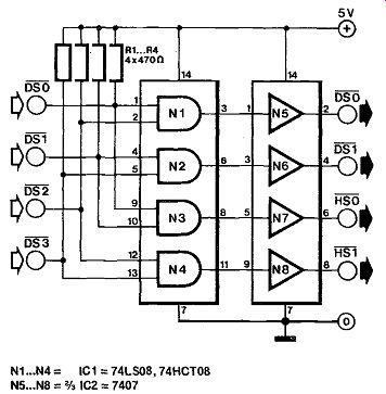
The Shugart standard supports the use of four disk drives, which are selected with drive select lines DS0-DS3. Two further lines, HS0 and HS1, control the head selection on each of these drives. When this circuit is installed between the computer's disk controller output and two double-sided drives, the disk operating system (DOS) can recognize four logical drives. When the computer selects drive A or B, the situation is similar to before the conversion. Selection of drive C or D, however, causes the second head in the relevant drive A or B to be activated. In this way, the total storage capacity of the double-sided drives is available even under "primitive" circumstances.
Note that the use of drive denotations A-B-C-D or 0-1-2-3 is particular to the type of computer, or the DOS version. Finally, Table 1 provides information about the combination of the original four DS lines into two HS and two DS lines.
065 FILTERED CONNECTOR
Computers and computer-driven peripherals are notorious sources of RF interference, and receiver jamming may occur at frequencies well above 100 MHz, even though the computer is said to run at a mere 16 MHz or so. The cause of this problem lies in the very fast pulse rise time of the switching and timing signals internal and/or external to the computer system and its peripherals, which are often located well away from one another (printer, modem, mass storage).
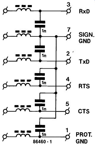
Much of the interference originating from long peripheral wiring systems may be suppressed quite effectively by inserting simple low-pass filters in the signal lines for data and handshaking. The proposed L-C filters are composed of small (3 mm) ferrite beads with 10 turns of 0.2 mm (36 SWG) enameled copper wire, plus a ceramic 1 nF capacitor; the coil inductance is about 80 µ}1, which gives a cut-off frequency of about 60 kHz (120 K-baud).
The filters are mounted on a small piece of Veroboard which may be cut and filed to fit into a standard D-connector housing. Other cut-off frequencies may be defined by modifying the small coils; inductance is proportional to the square of the number of turns, while constructors boasting of good (near) eyesight and lots of patience may endeavor to use thin (0.05 mm) copper wire to run through the beads. However, the L-C ratio as given should not be modified.
In conclusion, it should be noted that a filtered connector dimensioned for, says 10 kHz, should not be connected to a high frequency (20 MHz) computer output, since the excessively high capacitive load may cause damage to the line driver IC.
--------
066 FLOPPY CENTRING UNIT
In modern disk drive mechanisms, as, for instance, the TEAC FD55x, the motor starts automatically when a disk is inserted into the drive. When the lid is closed, the motor stops again. This arrangement ensures better centering of the disk. Better centering means less wear on the center fixing hole, the life of the disk is extended, and read/write errors owing to eccentricity off the disk are prevented.
Owners of older drive mechanisms, such as the BASF 6106, can incorporate that facility with the circuit proposed here. The signal from the write protect phototransistor is used to determine when a disk is being inserted (this signal is normally gated when the drive is closed), and to start the motor for the total period of monostable MMV1. The SPEED signal is not absolutely necessary: it stops the motor direct when the lid is closed. If it is not used, pin 3 must be connected to the + 5 V line.
The motor will then run for the duration of the period of MMV1, i.e., about 10 s. The monostable period can be reduced by lowering the value of the capacitor.
The points where to connect the circuit in the 6106 are easy to find. Looking at the pcb from the front, you will see a cut-out in the front center of the board. Immediately to the left of this are three ICs (see photograph). The one at the front is a 7474, the one in the middle a 7432, and the one at the back a 7404. The signal SPEED is taken from pin 6 of the 7474, and the signal D1 from pin 2 of the 7404.
The signal MOTOR ON is applied to pin 3 of the 7404. As all existing connections remain, the connecting wires of the auxiliary circuit can be soldered direct to the relevant IC sockets. In the same way, it is possible to derive the supply voltage for the auxiliary circuit: for instance, +5 V from pin 14 of the 7404, and 0 V from pin 7 of this IC.
It is important to note that there are two types of pcb used in 6106 drives: the ICs and the IC function are the same in both versions, but the construction may look different .
-------


067 FLOPPY DISK DRIVE
This is a much simplified version of the circuit published in the April 1984 issue of Elektor Electronics, but it is, unfortunately, not usable with all disk drive motors.

--------
First, a recap of the operation. The drive motors are switched on when one of the drives is accessed by a DISK SELECT signal. There is a delay of a few index pulses before access proper to give the motor speed time to stabilize. A few seconds after all the drives have been deselected, the motor is switched off. This arrangement reduces operation of the drive mechanisms, the heads, and the disks to a minimum, which ensures a longer life of these devices.
In contrast to the earlier published article, the READY output of the drive mechanism is used, wherein lies the reason that the older circuit cannot be as compact and simple as the present one: it has to take into consideration that not all drive mechanisms have this output. However, as far as we can find out, most drive mechanisms do have it, but there must be some, of course, that do not.
Figure 1, which is part of the circuit of the floppy controller board (Elektor Electronics, November 1982), shows the new wiring of port A7. The x at plug PL2 represents pin 3 of the type FD-55x drive mechanism, and pin 6 of the BASF 6106. As this latter input corresponds to Disk Select 4, not more than three BASF 6106 drives can be connected to the present circuit.
It is a wise precaution to break the connection between pin 10 of gate N25 and pin 6 of PL2, but it is not strictly necessary. As long as you do not select drive 4 (with the Ohio DOS, drive D), nothing can go wrong.
One connection that must be broken is that between pin 16 of PL2 and earth. Instead, pin 16 must be connected to pin 8 of IC2 as shown in figure 2.
If you are really a dab hand at soldering, you may be able to make the changes, with the appropriate lengths of wire, on the relevant printed circuit board. Most of you will, however, find it much easier to use a 15x20 mm piece of Veroboard, which after completion can be glued or screwed on short spacers underneath C16 on the floppy controller board.
068 HEXADECIMAL KEYBOARD
There are various ways of producing a hexadecimal keyboard. Normally, it is based on a number of key contacts in a matrix, but here a rather simpler method is used: 16 key contacts (0 . F) that are commoned to the positive supply line. Such keyboards are commercially available.
Code conversion is carried out by two priority en coders, IC3 and IC4. If one of the inputs Io . I7 of these ICs is connected to the positive supply line via one of the contacts S1 . .S16, i.e., made logic high, the relevant binary code appears at the associated output, Q0... Q2, of which Q0 is the least significant bit (LSB). As the encoders are cascaded, there is a total of 16 inputs.
Corresponding outputs of the encoders are combined in OR gates N6 . . N8 to form the lowest three output bits D0 . D2. the fourth data bit is taken from the GS (group select) output of IC4. This output is logic high when one of key contacts Ss . . .S16 (8 . . . F) is closed.
As the GS outputs of the two ICs are combined in OR gate N5, D3 is active high when a key is pressed.
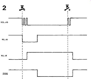
The signal at pin 9 of N3 is delayed by R18-C2. At the same time, the signal at pin 15 of IC3 triggers monostable N1-N2. During the pulse period of about 10 ms, pin 8 of N3 is logic low so that, in dependent of the delayed signal at pin 9, the output of N3 remains logic high. If pin 9 of N3 is still high when the pulse begins to decay, the output of N3 goes low and remains so until pin 9 becomes logic 0 again. During this time, pin 6 of N2 remains low, so that the monostable cannot be triggered erroneously. The timing diagram in figure 2 further clarifies the operation, which results in a debounced strobe or strobe pulse.

------------
If more than one key is pressed, the highest is selected, as is to be expected from a priority encoder! The circuit requires a power supply of 3 . . .18 V: current consumption is not greater than 10 mA.
069 IMPROVED SOUND FOR THE BBC MICRO
-----------
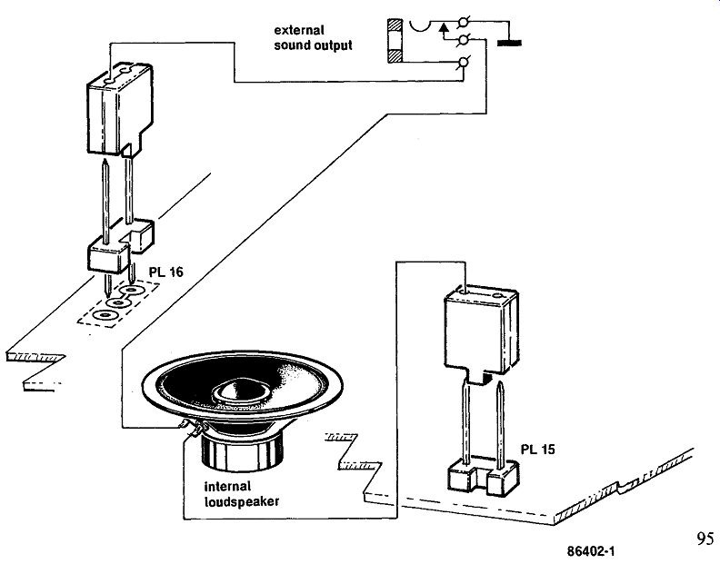
Despite the many laudable qualities of the BBC microcomputer as to speed and ease of peripheral interfacing, many users are slightly disappointed with the sound quality of the standard version as manufactured by the Acorn company. An investigation into this matter has revealed that Acorn have disregarded the optional connection of an external audio amplifier to the computer; this is the more surprising since special holes have been provided to this purpose on the main PCB. The result of this omission manifests itself in a very poor sound quality, caused by the small loudspeaker in the cabinet, the high noise level of the improperly driven audio amplifier chip, and the rather coarse volume setting.
However, a minor modification to the BBC computer is sufficient to boost its sound production by means of an external, more powerful audio amplifier which may be connected to a sound output socket on the computer. Proceed as follows:
1. Open up the computer, remove the keyboard and the main PCB.
2. Locate the PCB holes for plug 16, to the left of IC7, the Type LM386 audio amplifier chip.
3. Use desoldering braid to open up the holes for plug 16, if these are filled with solder.
4. Cut off the center pin of a three-pin, 0.1 inch pitch single row PCB header, and solder it in the holes provided for plug 16.
5. Mount a 3.5 mm jack-type audio socket with a break-contact at the rear side of the computer, and wire P16, P15, and the internal loudspeaker as shown in Fig. 1.
6. Reassemble the computer and test the new audio output by connecting an external amplifier set to the jack socket. Insertion of the jack plug should silence the internal loudspeaker.
Now that we are on the subject of the BBC computer, it is just as well to give a few hints concerning reduction of the total power consumption of the computer. The Type 6522 VIA chips may be re placed with their new CMOS equivalents 65C22 to reduce the total current consumption by some 240mA. The 6850 chip may also be replaced with a 6350, but this is a riskier matter since the former chip is soldered direct onto the PCB.
070 JOYSTICK ADAPTOR
Some popular computer games require the joystick to be turned 45° in order to get the correct cursor movement on the screen. Obviously, this presents problems if the joystick is desk mounted or of the type that is ergonomically styled and hand-held.
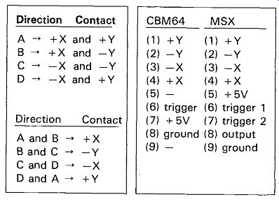
The electronic solution to this inconvenience starts from a redefinition of the joystick axes, as shown in Fig. 2. Direction A is defined as in between the positive X and Y axes; direction D as in between the negative X and positive Y axes. Directions C and B are opposite to A and B respectively. Table 1 summarizes the old and new direction assignments and associated activated outputs.
The circuit diagram of the adaptor circuit- Fig. 2 - shows that the output levels to the computer are active low rather than high as in the unmodified joystick connection; this necessitates the use of inverter gates between adaptor and computer input.
A Type 74LSO4 hex inverter may be used to this end, and the trigger (fire) function(s) can also be inverted at the same time, since this IC contains six inverters.
The double trigger function enables the turned joystick to be connected to MSX types of computer as well. Table 2 lists the relevant connections for both the C64 and the MSX computer type.
The adaptor input and output signals may be visualized with red and green LEDs, clearly indicating the electronic signal turn over 45°. When the joystick is moved into direction A, for instance, input LED + Y lights, as well as output LEDs + Y and +X. Current consumption of the adaptor circuit is about 75 mA.
Table 1
Table 2
---------
071 LEVEL ADAPTOR FOR ANALOG JOYSTICK
An analog joystick usually contains two potentiometers, whose wipers are controlled from the central handle on the unit. Unfortunately, the angle covered by the handle is generally only about 90°, whereas the potentiometer's spindle and wiper can be rotated over 270°. The voltage range provided by a potentiometer in a joystick is, therefore, relatively small. Two of the circuits described here make it possible to enlarge the output voltage range of both potentiometers in the joystick. The circuit is readily doubled, thanks to the use of dual CMOS operational amplifier Type TLC272.
Each of the two wiper voltages from the joystick is processed separately, which enables interesting effects to be achieved. The amplification of the circuit is determined by P3. This preset enables the enlarging of the potentiometer's "range" to individual requirements. Preset P2 serves to shift the operative range of the potentiometer within the limits of the supply voltage, which may lie between 3 and 16 V.
Setting up this circuit is straightforward. Commence with setting P3 for minimal resistance, i.e., A1 should give unity gain. Set the joystick handle to its center position, so that the wiper of Pi is at mid-travel. Adjust P2 to make the output voltage of the circuit equal to V2Vdd. Move the joystick handle to the outer positions in the relevant plane, and note the corresponding output voltages from the circuit. Adjust P3 such that the circuit outputs the required voltage span. The adjustment of P2 enables changing the toggle point of the circuit, that is, the voltage it outputs when the joystick handle is set to its center (rest) position.
The current consumption of the circuit depends on the supply voltage level, and also on the value of Pi When Vdd = 5 V, and P1= 4K7, the current drain is less than 10 mA. The Type TLC272 was chosen because it works fine from a single supply voltage, and also because it has an extensive input voltage range, 0 to Vdd-1.5 V.

------------
072 LISTEN-IN KEY FOR DATA RECORDERS
The pros and cons of using data (cassette) recorders for mass memory storage in a computer system are likely to be so well-known that any further discussion as to the relative cost efficiency of the cassette tape would seem to be superfluous.
There is, however, one distinct disadvantage to the data recorder that is relatively easy to get rid of, viz, the trouble many users experience in positioning the tape to the leader note of the desired program or file to load into the computer. Many data-recorders, while offering the highest possible save and load speed, fail to produce the sound on tape when the computer audio cable is plugged into the earphone socket, forcing the user to plug and unplug this cable in a desperate search for the program.

----------
The solution to this sorry plight consists of a simple combination of resistor and push to make button, which are to be built into the cassette recorder. The circuit diagram shows the method of connecting these parts; pressing the button with the earphone plug inserted in the socket will enable the user to listen to the recorded data as the tape is played. The value of the resistor may have to be adapted to suit the specific output power of the data recorder, given the optimum playback level for the computer.
Now that you have opened the recorder for the outlined modification, it is just as well to mount a second button enabling tapes to be wound and played while the remote control plug rests inserted in the associated socket; this simple modification may also be of appreciable interest for the improved efficiency in locating files on tape.
073 MAINS INTERFACE
This circuit is of use, for instance, when a computer is required to monitor a mains-operated equipment.
Opto-isolator TIL111 ensures complete isolation between the mains and the computer.

--------
With the mains on, during every positive half-wave a current of about 1 mA flows through the LED in the opto-isolator. The associated transistor then conducts and its collector current of about 100 µA is sufficient to drive T1. Remember, however, that this is a pulsating current: capacitor C1 ensures that T1 conducts continuously as long as the mains is on. If a 50 Hz square wave is required at the collector of T1, C, should, of course, be omitted.
The two 100 k resistors in series with the LED should not be replaced by one 220 k resistor, because the maximum permissible voltage drop across a standard 1/4 W resistor should not exceed 150 Vrms.
074 MANDELBROT GRAPHICS

--------------
The computer-based implementation of certain iterative types of calculation may offer highly at tractive graphics screen representations, as we got to know when keying in a program to crunch a few numbers in the Mandelbrot series, and found that doing so with the support of the computer's graphics facilities took us through a regular graphics adventure. On further investigation, it was found that the degree of complexity of the resultant graphics image is in direct proportion with the number of iterative steps the control program is arranged to perform. However, since the necessary calculations to obtain a Mandelbrot series become the more complex, and therefore time consuming, as the computer crunches through its approximations and evaluations, it should not strike the programmer as odd that obtaining a nicely detailed graphics image may take as long as 12 to 24 hours, even with the fastest types of personal or semi professional types of computer, such as the BBC equipped with a second processor.
The Mandelbrot series of numbers is basically obtained with the use of complex numbers, in a calculation that converges rather than diverges the intermediary results according to the equation Z=Z2+C, where C is the complex number constant having a real part between-2 and 1, while the imaginary part ranges between-1.5i and 1.51; Z is the result of the preceding calculation.
Stepping through a section of the series is possible by assigning start values and/or differently dimensioned step rates to either the real or the imaginary part of C. It goes without saying that calculation time and image resolution increase with the number of iterations used for obtaining results in accordance with the set requirements; the calculations may be stopped when the result is larger than 2. The color assigned to any pixel on the screen depends on the number of iterative steps required to satisfy the Mandelbrot equation; if this is not the case, the iteration loop is consequently aborted.
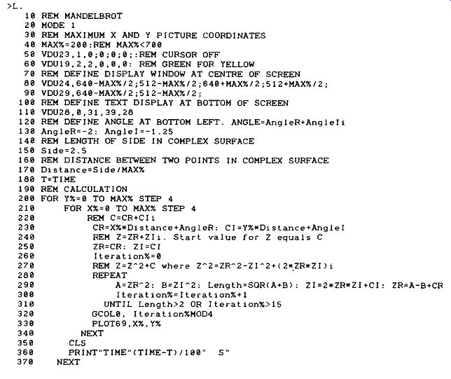
The program shown in Listing 1 has been written for the Electron or BBC computer, and arranges for 15 iterative steps; the screen-dump of Figure 1 shows the result. Figure 2 illustrates how a section of the graphics image is enlarged by means of relevant redefinition of the equation variables, as outlined above. Obviously, the suggested program allows a good deal of further patching and experimenting to arrive at even more attractively styled graphics designs, but it should be pointed out that producing Fig. 2 took our BBC no less than . . . 2 days!
Listing 1.
--------
>L.
10 20 30 40 50 60 70 80 90 100 110 120 130 140 150 160 170 180 190 200 210 220 230 240 250 260 270 280 290 300 310 320 330 340 350 360 370
REM MANDELBROT MODE 1 REM MAXIMUM X AND Y PICTURE COORDINATES MAX%=200:REM MAX%<700 VDU23,1,0;0;0;0;;REM CURSOR OFF VDU19,2,2,0,0,0: REM GREEN FOR YELLOW REM DEFINE DISPLAY WINDOW AT CENTER OF SCREEN VDU24,640-MAX%/2;512-MAX%/2;640.MAX%/2;512+MAX%/2;
VDU29,640-MAX%/2;512-MAX%/2;
REM DEFINE TEXT DISPLAY AT BOTTOM OF SCREEN VDU28,0,31,39,28 REM DEFINE ANGLE AT BOTTOM LEFT. ANGLE=Angle R+ Angle Ii Angle R=-2: Angle1=-1.25 REM LENGTH OF SIDE IN COMPLEX SURFACE Side=2.5 REM DISTANCE BETWEEN TWO POINTS IN COMPLEX SURFACE Distance=Side/MAX% T=TIME REM CALCULATION FOR Y%=0 TO MAX% STEP 4 FOR X%=0 TO MAX% STEP 4 REM C=CR+Cli CR=X%w Distance +Angle R: C1=Y%w Distance + Angle l REM Z=ZR+Z11. Start value for Z equals C ZR=CR: Z1=C1 Iteration%=0 REM Z=Z-2+C where Z-2=ZR-2-Z1-2,(2wZR.Z1)1 REPEAT A=ZR-2: B=Z1-2: Length=SOR(AwB): ZI=2*ZR*ZI+CI: ZR=A-B+CR Iteration%=Iteration %wl UNTIL Length>2 OR Iteration%>15 GCOLO, Iteration%MOD4 PLOT69,X%,7% NEXT CLS PRINT"TIME"(TIME-T)/100" S" NEXT
075 MORSE TRAINING WITH THE JUNIOR COMPUTER
Here is yet another small program to be added to the large amount of software already available for the Junior Computer. It is intended to teach prospective short wave listeners to read morse code.
The program can be used even with the basic version of the JC. The only additional hardware is the amplifier stage shown in the accompanying figure.
The input to this is taken from port line PB5.
The number and speed of the morse characters can be predetermined. After the program has started, the JC will generate 1 to 6 morse characters, which the trainee should decode and write down. The letters corresponding to the generated characters appear on the display after a short delay, so that the trainee can check his decoding with the actual text.
During this phase, the computer is on stand by until an arbitrary key, other than ST and RST, is pressed.
The hex dump given is sufficient to write the program into the JC. Once that has been done, you can prepare the start, but the program needs the following information before it can run.
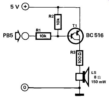
----------
in address 0010 write data 00 . . . 05;
in address 0011 write data 01. . .55 (max);
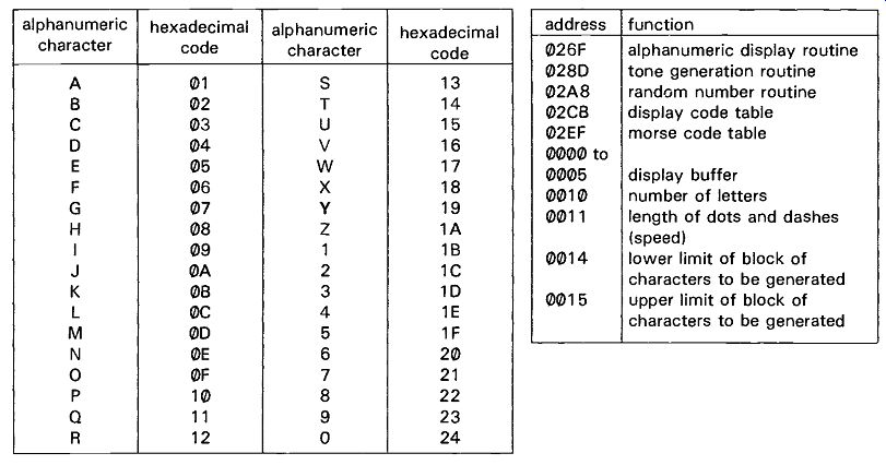
in address 0014 write data from table 1 for the first character to be generated minus 1;
in address 0015 write data from table 1 for the last character to be generated.
-------
Table 1.
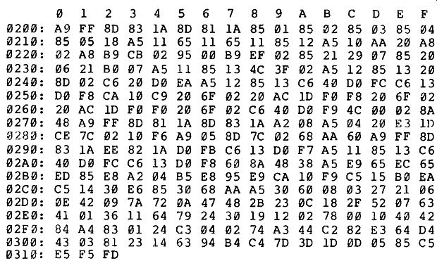
Table 2.
Now, the program can be run; it starts in address 0020 when key GO is pressed. Programming example: the JC is to generate morse characters for the letters B to G. Before the start, the following data should be written:
in address 0010- data 05
in address 0011- data 55
in address 0014- data 02
in address 0015- data 07
As soon as these data have been written, the program starts when key GO is pressed.
The hex data for the letters of the alphabet and numbers 0...9 are given in table 1. The most important addresses are given in table 2.
076 PIA FOR ELECTRON
Despite its neat design and relatively low cost, the Acorn Electron computer suffers from an unfortunate lack of I/O support, which is remarkable, considering the fact that it is a relatively simple matter to add, say, two I/O ports to enable the computer to drive a printer, plotter, modem, or other peripherals by means of the proposed PIA (peripheral interface adapter).
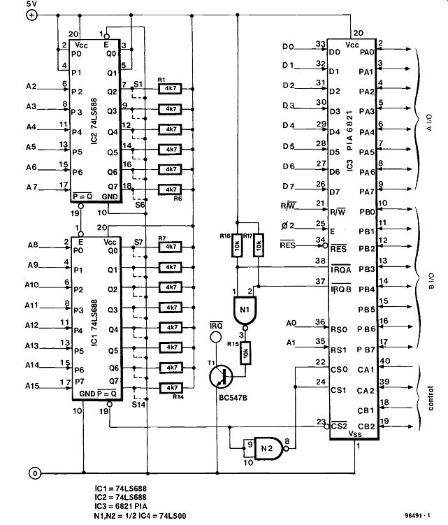
-----
The circuit diagram of the PIA-based extension shows that address decoding over the full 64 Kbytes is by means of two 8-bit magnitude comparators Type 74LS688. Address selection is manual with switches S, . .S14, which provide a logic low level when closed; observe this when writing out the ones and zeros to arrive at the desired address in the I/O map. The PIA chip is enabled when the preset address matches that on the computer's address bus; writing simple I/O drivers is there fore mainly a matter of assigning the relevant ad dress block to control words and PIA I/O data.
T1 has been included to enable the PIA circuit to generate and forward interrupt request pulses by means of the wired-OR arrangement for this control line.
In case it is desirable to switch heavier loads than is normally permissible with the PIA outputs, it is suggested to employ power drivers/inverters such as those in the ULN2000 series.
077 QL RAM EXTENSION
---------
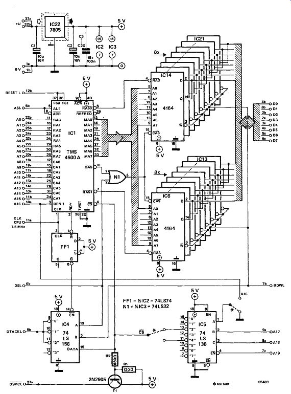
Sinclair's QL has as standard a 128 K RAM, which sounds like a lot in comparison with most 64 K machines. Unfortunately, the software writers, in the knowledge that there is more than enough memory, have been rather wasteful in their work, so that at the end of the day, there is not all that much more in the QL than in the 64 K machines. So, you need more memory . .
The accompanying circuit is an application of the TMS4500A as RAM extension for the 68008. This chip can drive a maximum of 128 K dynamic RAM and provides virtually everything: multiplexing of the address lines, RAS, CAS, and REFRESH.
The memory ICs are 64 K x 1 (128 or 256 refresh are both permitted) and have a speed of better than 150 ns. Since the QL uses a clock frequency of 7.5 MHz rather than the normal 8 MHz, such a RAM can run without wait cycles. An 8 MHz CPU that regularly has to carry out a wait cycle is appreciably slower than a 7.5 MHz type! The 68000 family is provided with a data acknowledge input. As with other processors, the CPU places addresses and data onto the bus and indicates the validity with an address strobe and data strobe respectively. It continues to do so until the memory sends a DTACK signal. The present extension generates this signal with the aid of the LS156.
Normally, this acknowledgment is given almost immediately, but it may happen that the 4500 is in the middle of a refresh. In that case, the CPU has to wait, which is arranged via the ready output (pin 2).
To prevent the QL waiting forever when an address is read that has no memory, the DTACK is generated internally: this must, however, be disabled for addresses where the RAM extension is located, and fortunately this can be done easily via DSMC. By making this logic high as quickly as possible, the internal DTACK is cancelled.
If you cannot get the 2N2905 transistor, you may use a BS250, in which case resistor R can be omit ted and R2 should be replaced by a wire link.
The circuit as shown is for the 128 K version. It is also possible to omit the eight RAMs connected to RAS1 and make a 64 K extension. Input A of the LS138 must then be connected to A16 and pin 11 instead of pin 13 must be used as CS.
There is no 5 V supply available on the connector, but there is a 9 V line. This can be reduced to 5 V by a standard 7805. The current drawn depends on the types of RAM and will be 200 ... 300 mA. It is important to decouple the supply lines properly: each RAM IC and the 4500 require a 100 n capacitor!
078 RAM EXTENSION FOR QUANTUM LEAP
The Sinclair Quantum Leap (QL) computer is eminently suitable for a low-cost introduction into working with Motorola's 68000 true 16-bit micro processor. Many computer enthusiasts did not fail to note the spectacular price cuts for the QL when its production was discontinued. An excellent support program, TOOLKIT II, became available and is still considered indispensable by many for getting to grips with the QL. The present 512 Kbyte RAM extension should be very welcome for running a RAM disk, and/or programs such as ICE and QIMP.
The circuit is based around the Type THCT4502 RAM controller from Texas Instruments. This dedicated controller takes care of all the DRAM controlling, including the refresh timing, and the address line multiplexing. The address decoder is made with a single XOR gate, N7. The DSMCL line is made high within 30 ns with the aid of three-state buffer N5. Bistable FF1 delays the ASL signal somewhat, so that DTACL is only activated when the RDY output of IC: is stable. The databus is buffered by bidirectional octal transceiver IC23.
The extension memory is divided in two banks of 256 Kbyte. Note that CAS, unlike WKS-, is common to both banks. It is possible on the QL to omit the second bank without altering the address decoding.
This is thanks to QDOS, which searches for correctly operating continuous, and unique, i.e., non-mirrored, memory. It is interesting to note that machine code in the extension memory runs at almost double the normal speed.
The RAM chips used should have an access time of 150 ns or less. Current consumption of the extension is low at 50 mA or 150 mA in the non-active and active mode respectively. Non-used inputs on gates should be tied to ground.
Finally, note that the Type THCT4502 controller may not be available everywhere yet.
Distributor for TI Semiconductors in the UK is DC Distribution Freepost Hitchin Road Arlesly Bedfordshire SG156BR. Telephone: (0462) 834444 or (0454) 273333.

--------------
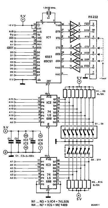
079 RS232 INTERFACE
This circuit is intended as an interface between the Elektor modem (Elektor Electronics, October 1984) and a computer. The software for each individual computer must, of course, be written separately.
Since the writing of a terminal program can only be carried out in machine language, the interface can be kept quite simple.
Signals at TTL level are sufficient to operate the modem and LSO5 buffers are therefore used. Complete address decoding of the 6551 is ensured by IC2 and IC3 so that only four locations in the memory are required, and these should be available on virtually any computer. The fourteen common address bits are selected with S1 .S14: a closed switch represents an address bit or 0. The input buffers are standard RS232 line receivers so that they can cope with any voltage levels that may be present on an RS232.
The interface is also suitable for connecting a serial printer to a computer, provided it can operate from TTL levels, which normally is the case.
The accompanying tables show some of the possibilities of the 6551 and are intended as an aid in the writing of the terminal program.
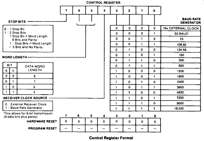
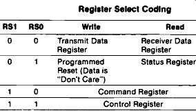
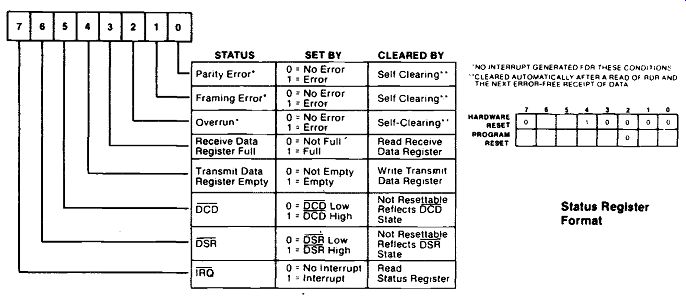
----------- Register Select Coding
Note that only the Command and Control Registers can be accessed during both Read and Write operations. Programmed Reset operation does not cause data transfer, but is used to clear (reset) all G65SC51 internal registers. Programmed Reset is used in a slightly different way as compared to the hardware Reset (RES). These differences are described under each individual register description.

---------
080 SAMPLE & HOLD FOR ANALOG SIGNALS

--------
Conventional analog sample and hold circuits are notorious for their tendency to drift, a phenomenon unknown in digital memories. It is, therefore, interesting to study the use of a digital memory element for storing an analog signal.
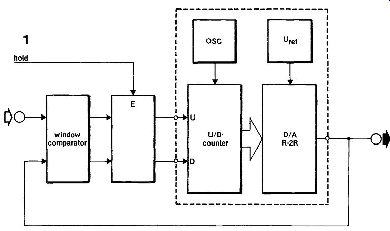
The present circuit is based on intermediate storage of digitized analog information, and therefore re quires an analog-to-digital converter (ADC) at the input, and a digital-to-analog converter (DAC) at the output. Unfortunately, DACs and ADCs are typically expensive components, and the present circuit is therefore set up with a DAC only, driven by an up/down counter-see Fig. 1. The counter is essentially an ADC, since the output voltage of the R-2R based DAC is continuously compared to the input voltage with the aid of a window comparator.
The error signal produced by the comparator arranges for the counter to count up or down, de pending on the magnitude of the difference between the input and output voltage. The up/down counter is corrected until the input and output voltage are equal. The digitized result of the A-D conversion is available at the counter outputs.
The extensions for converting the basic set-up into a sample & hold circuit are relatively simple. The current count is retained by activating the HOLD input, which enables halting the U/D counter. Evidently, the counter state is not subject to drift, so that the analog output signal is available unaffected for as long as the circuit is powered. The converter used here is the Type ZN435 ADC/DAC from Ferranti. This chip contains everything shown in the dashed box of Fig. 1. With reference to the practical circuit diagram, Fig. 2, the internal voltage reference and the oscillator are adjusted with R1-C1 and R2-C2 respectively. The later are dimensioned for 400 kHz, i.e., nearly the maximum oscillator operating frequency. The internal counter is controlled via inputs up , down and mode. The logic level applied to the mode input determines whether the counter continues or halts upon reaching state 0 or the maximum value, 255.
In the present application, the counter is halted.
Gates N1 and N2 are added to enable blocking the U/D counter. Opamps A,-A2 form the window comparator. Current source T1-R7 and R6 arrange for the toggle threshold of A1 to be 20 mV higher than that of A2. This off-set creates the window, or inactive span, needed to suppress oscillation of the counter's LS bit, and to prevent unwanted effects arising from the comparators' offset voltages.
Decoupling capacitor C3 is fitted for suppressing spikes that occur during state changes on the counter outputs. The conversion time of this design is about 640 pis, as determined by the oscillator frequency (400 kHz), the resolution (8 bits) and the in put voltage change (2.55 Vpp max.). This corresponds to a slew rate of 4 mV/µs at the input. Finally, bear in mind that the output impedance (IC1, pin 11) is relatively high at about 4 kg.
081 SERIAL DATA CONVERTER
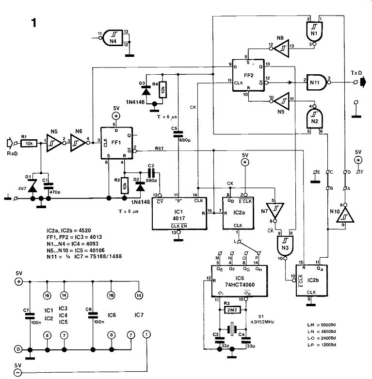
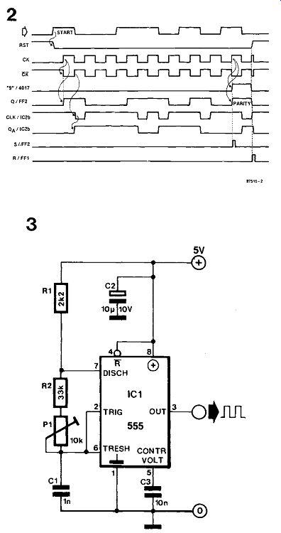
-------
Some computers and communication programs are unable to output serial data composed of 7 data bits and a parity bit. The present circuit has been de signed to output this data format when it is driven with serial data organized as 1 start bit, 8 data bits, no parity bit, and 1 stop bit. This format is widely used for accessing bulletin boards, data banks, and the like with the aid of a modem, and should be available on most computers equipped with an RS232 port. The converter has a built-in clock generator which can be set to the baud rates shown the circuit diagram, Fig. 1. Both odd and even parity can be generated, and no handshaking is required with the computer or console.
The basic operation of the converter is as follows (also refer to the timing diagram in Fig. 2). The rising edge of the start bit in the incoming 10-bit word clocks bistable FF-I, whose output ohm goes low and so enables counters IC1, IC2a and IC2b, which were previously blocked by the high level of RST. Binary counter IC2a starts counting the clock pulses provided by baud rate generator IC6. The frequency of this clock signal is 16 times the bit rate on the serial input and output line. Bistable FF2 and counter IC1 are clocked with signal CK, whose period corresponds to that of the bits in the data stream. The received start bit and the next seven data bits are passed through FF2, while IC, keeps count of the number of transmitted bits, and actuates output 9 during the reception of the ninth bit (i.e., databit 7).
The rising edge of the counter output pulse is differentiated in C5-R6 and then applied to NAND gates N1-N2. These make it possible for FF2 to be set or reset, depending on the state of parity counter IC2b, which keeps count of the logic high bits in the serial word applied to the converter. Its output QA indicates whether the number of detected high bits is odd (QA =1) or even (QA = 0), and causes FF2 to toggle when the differentiated pulse from IC, makes the output of N8 or N6 go high for a very short period. When QA is low, the parity bit at ohm of FF2 is high because in that case the S (set) input is driven high. Similarly, the parity bit is low when QA is high because the R (reset) input on FF2 is then driven high. These two situations can occur when even parity is selected by fitting wire links A-D and B-C as shown in the circuit diagram. Odd parity is obtained by fitting links A-C and B-D, and permanently low parity by fitting C-E and D-F (note that a "low" parity level means that the relevant bit is logic high in the RS232 convention).
After transmission of the parity bit, the circuit is prepared for the next word by the carry (CY) output of IC, providing a high level to differentiator C2-R4.
This resets FF1, which in response drives the RST line high to reset the counters.
The convention adopted for the logic high and low levels of the data bits in the proposed converter re quires that this is inserted in an RS232 or RS432 data line. Line driver Nil may be omitted, and the serial output signal taken from ohm on FF2, if the driven input can operate with pulse levels of 0 and +5 V.
Finally, Fig. 3 shows a suitable alternative for the crystal-operated clock generator, which may be considered too extensive if the circuit is to work at a fixed baud-rate of 1200. Multiturn preset P1 is set for an output frequency of 19,200 Hz.

----------
082 SERIAL LINE DRIVER AND RECEIVER
This circuit owes its existence to the need for data communication over relatively long distances (up to 100 meters), inexpensively, reliably, and suitable for speeds up to 2400 bauds. At the distances considered, the main expense is normally the cable, so here a readily available 60-ohm coaxial cable is used.
Because of its relative immunity to noise, current drive is employed.
In the line driver--figure 1--transistor T1, di ode D4, and resistors R3 and R4 form a current source that can be fed direct from a non-regulated supply of 8 . . .10 V. The transistor should be mounted on a heat sink. The current level of 40 mA ensures an adequate input signal to the line receiver.
Transistor T2 is a current switch that short-circuits the current source and the cable to earth of the in put to the driver is logic high: only when that input is logic low, is the current of 40 mA fed into the cable. Diodes D2 and D3 protect the driver against noise emanating from the cable, while capacitor C1 decouples the supply line.
The line receiver is based on a type LM 311 comparator. Matching of the input is effected by a wire link at a relevant tap of resistive divider R5-R6 R7/R8 (in our case: 60 ohm). Resistors R9 and R10, and diode D5 protect the LM 311 against noise emanating from the cable. The sensitivity of the receiver is set with Pt. Resistor R14 provides some hysteresis. Pull-up resistor R15 ensures that IC, provides at its pin 7 a TTL output signal that is in phase with the input signal to the line driver.
The circuit is best calibrated with the aid of an oscilloscope once it has been installed in its final position. The level of input to the receiver is then compared with the voltage at the wiper of Pt The set ting of Pi is optimum when the voltage at its wiper (wave form A in figure 3) is exactly opposing the in put voltage (wave form B in figure 3).
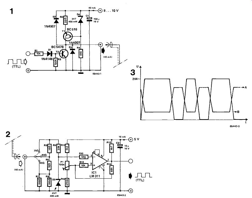
---------
083 SIDEWAY RAM FOR BBC AND ELECTRON PLUS ONE
As already reported on numerous occasions in Elektor Electronics, the BBC micro ranges among the most widely used types of personal computer currently available. To newcomers in the computer field, the amount of commercially available ROM-supplied software is truly staggering, and there seem to be programs to suit almost any requirement and budget.
However, the number of ROMs that may be located in the BBC computer is limited to four in the basic version and sixteen when it is equipped with a sideway ROM expansion card. Users in possession of a good many ROMs and EPROMs are, therefore, often forced to exchange these before a program can be run; a method that is both cumbersome and possibly bad for the ICs and their sockets.
A way of getting round this problem is to install RAM rather than ROM or EPROM chips on the sideway board, so that software may be readily moved about between ROMs, direct access memory, disk and RAM, since many of the originally ROM-based programs may also be run from RAM, it has appeared.
Since it was thought convenient to plug 16 Kbytes of static RAM into any one vacant ROM socket, the circuit was constructed in all-SMD technology on a ready-made PCB of very small size.
The circuit diagram shows two 8 Kbyte, low-power static RAMs Type 6264FP-15 as a replacement for a 16 Kbyte EPROM Type 27128; a single inverter selects the relevant 8 Kbyte block when the (formerly) ROM socket is addressed.

---------
Working with SMD parts to achieve a truly miniature ROM replacement should be based on the necessary skills in soldering and handling these new parts, and the construction of the proposed extension therefore requires to be done as follows.
It should be noted that the through-plated PCB for this project comes together with the SMD die.
Fit 28 short (1 cm) pins at the sides of the PCB to enable it to be received in an IC socket.
The SMD RAMs are mounted piggy-back onto the PCB, with the exception of pin 26 of the top mounted RAM; this terminal should be wired to socket pin 28. The SMD parts 74HC04 (IC3) and R I may now be fitted to conclude the PCB construction. Once the unit has been plugged into a ROM socket, a short wire is run from pin 8 of IC77 on the BBC main board to the NWDS input on the SMD board.
Parts list
R1 =100 k
IC1;IC2=6264FP-15
IC3=74HC04
PCB 86425
Miniature switch for write protection, if required.
Finally, although not mentioned so far, the Electron Plus One computer may also benefit from the pro posed sideway RAM circuit which, as will be readily understood, need not necessarily be constructed with SMD parts; a veroboard and normal sized components, along with a bit of wiring, will also do in many cases, although it may be hard to surpass the elegance of the plug-in unit.

--------
084 SIMPLE D-A CONVERTER
Two simple to build 4-bit digital-to-analog converters are described here. One translates a 4-bit BCD code into 10 analog voltage levels, the other accepts a 4-bit binary code and outputs 16 voltage levels. Both circuits comprise a digital decoder with open collector outputs for controlling a resistance ladder. The analog voltage is obtained by con trolled connection to ground of a particular section of the ladder, and buffering the drop so obtained with a transistor.
Notwithstanding their relatively low resolution (10 or 16 steps), the circuit should have many possible applications, including driving digitally controlled power supplies, triangular wave and sawtooth generators, and A-D converters.
Table 1 lists the relative values of the resistors in the ladder network, starting from R, =1K-O. Three values are given for each resistor: the left-hand column shows the theoretical value, while the nearest equivalent from the E24 and E96 series appears in the center and right hand column, respectively.
Note that the starting value can be changed to individual requirements, provided all other resistors are dimensioned accordingly, i.e., their values should be multiplied with the same factor with respect to 1 K-O.
It is a relatively simple matter to add an 11th or 17th output level by driving the decoder such that none of its output transistors is enabled. This results in an output voltage which is 0.6 V lower than the supply for the ladder network. In the case of the 74LS145, this condition is obtained by applying a non-valid code to the inputs, i.e., one greater than 910 (10012). Similarly, on the 74159, enable input GI or G2 can be made logic high.
Table 1 Resistor values relative to 1 10


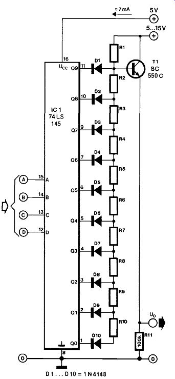
-----------
085 SIMPLE VIDEO INVERTER FOR ZX81
The inverter must be connected before the TV modulator in the ZX81. Switch S1 enables bypassing of the inverter when inversion of the picture is not required. The composite video signal is inverted by gate Ni. Gates N2 and N3 separate the sync signal from the input: the sync signal is then available at the output of N3 at a level of 5 Vpp.
The inverted video signal and amplified sync signal are then added again, resulting in an inverted video signal with the sync signal in the correct position and at the right level. Preset P1 serves to adjust the contrast.
The circuit can be constructed on a piece of veroboard so small that it can easily be added in the ZX81 case. The power supply can be taken from IC1 in the ZX81: +5 V at pin 40 and earth (0 V) at pin 34.
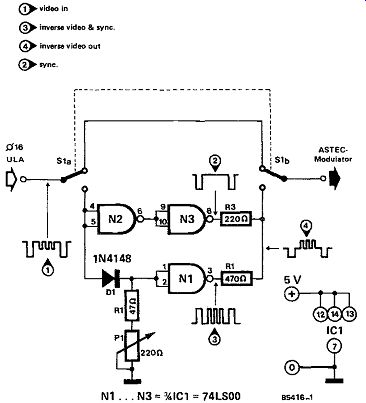
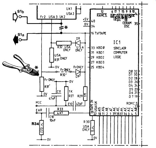
---------
086 SYNC INVERTER FOR THE QL
For some unknown reason, the Sinclair QL (and perhaps some other personal computers) provides positive, instead of the usual negative, field synchronizing pulses to the monitor. Inverting these pulses with a suitably fast NAND gate or inverter is, of course, no problem. What is a problem is where to power this gate from: a special supply would be nonsense. However, in the circuit proposed here, the gate is supplied from the sync signal itself. A monitor with TTL input for the sync signal draws only a very small current at logic 1, so that the additional load presented to the input pulse by the diode and electrolytic capacitor is inconsequential.
Instead of the HC-MOS gate shown, it is also possible to use a buffered CMOS gate, for instance, a type HEF4011B. Standard CMOS devices, such as the 4011, cause a very small delay, which in practice does not matter, and certainly not with a field sync signal. Note that it is important, as always with CMOS devices, to connect unused pins to earth (pin 7) or to Ub (pin 14).

087 SYNCHRONIZATION SEPARATOR
Many monitor chassis currently offered by computer surplus stores have separate inputs for horizontal and vertical synchronization signals.
Most home micros, however, have a composite video output, so that some form of interfacing is required to drive these bargain monitors.
The Type TBA950-2 is a sync separator chip which is frequently encountered on TV chassis. In its standard application circuit, it requires to be driven by a flyback signal derived from the output of the line frequency oscillator. Without this signal, which is applied to pin 10, the sync pulse would end up somewhere among the picture lines. To be able to use the TBA950-2 in the present application, the horizontal pulse is slightly shifted with the aid of a double monostable multivibrator, IC2.
The operation of the circuit should be clear from the accompanying timing diagram. The output pulse from the TBA950 is fairly wide (26 pis), and its positive edge triggers the first MMV (Q1), whose negative output pulse transition in turn triggers the second MMV in the 4538 package. The line sync pulse for the monitor is available positive and negative at IC2 outputs Q2 and Q2, respectively.
Adjust the circuit as follows: set P2 to the center of its travel, and adjust the frequency control, P1 , such that the image is stable. Next, position the image by adjusting P3. If the correct position can not be obtained, the phase control, P2, must be carefully readjusted, followed by P3. The vertical sync pulse is available at pin 7 of the TBA950-2. Finally, the dashed resistors and diodes are required if the monitor inputs are designed to accept signals with a peak-to-peak amplitude of 5 V.
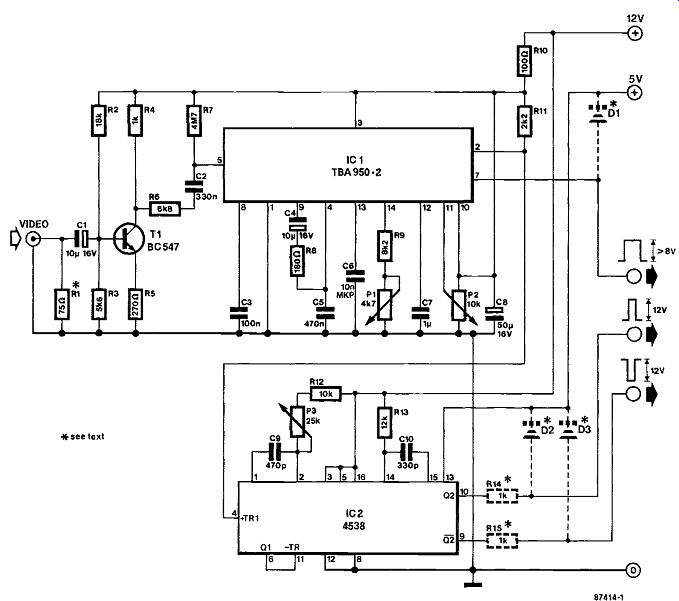

088 TWIN KEYBOARD FOR APPLE II
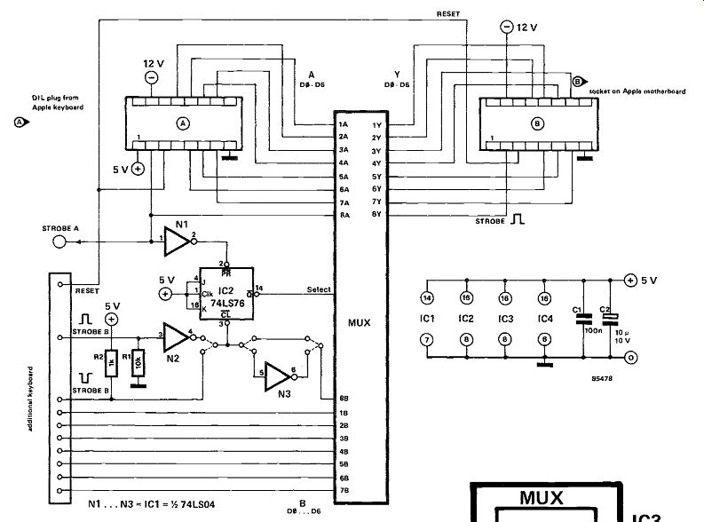

The keyboard supplied with computers is for many applications not the ne plus ultra it is claimed to be. Unfortunately, deficiencies normally do not become apparent until the machine has been in practical use for a while. Retailers have long since realized this and often stock improved keyboards that are fully compatible with the computer in question. It is, however, not always clear how the new keyboard can be attached to the computer. One possibility is, of course, to open the computer, remove the existing keyboard, install the new keyboard, and put the computer together again. It is, however, much better to use the solution suggested here, which is aimed at the Apple II and compatible machines.
The accompanying circuit makes it possible to connect the additional keyboard in parallel with the existing one. Basically, it is just an electronic switch-over unit, designated MUX in the diagram.
Both keyboards are connected to the input of MUX by their data lines. Which keyboard data are applied to the computer is from now on determined by MUX.
When a key is struck, the keyboard does not only generate data bits, but also a strobe pulse. Depending on whether the strobe pulse emanates from the original or from the additional keyboard, the Ty output (pin 14) of bistable IC2 is set or reset. This pulse, therefore, serves as a select signal for the MUX. The electronic switch consists of two type 74LS157 ICs.
Each of these ICs contains four 2-to-1 multiplexers, so that all eight input data are available at the output. If the select input of both ICs is logic 0, outputs IY . 8Y contain the data present at inputs IA . . . 8A. If, however, the input to the ICs is logic 1, the data from 1B . . 8B is available at 1Y . . . 8Y.
The Apple II requires a positive strobe pulse, and inverters N2 and N3 are, therefore, provided to ensure that this condition is met whatever the strobe pulse from the additional keyboard.
089 TWO-FREQUENCY CLOCK
Many computer systems use one clock signal, from which all other timing signals are derived. The frequency of the clock signal determines, among others, the maximum number of characters per line the video controller can display on the monitor screen. This is normally 32 or 40. If more characters per line are required, the clock frequency has to be increased. The clock generator described here makes it possible to switch between frequencies which are related in a ratio of 2:3. The switching is carried out synchronously, so that no bits are lost.
The clock oscillator, T1, is controlled by an inexpensive 3rd overtone 27 MHz crystal, XL,. The LC circuit connected to the collector of T, is tuned to 54 MHz. The 54 MHz signal is converted to logic bits by field-effect transistor T2 which are then applied to the ohm inputs of dual J-K bistable IC, ( = FF1/FF2). The ring counter formed by these bistables can be changed over by T3.
When T3 is on, the J input of FF, is logic high, and the 54 MHz signal is divided by 2. When T3 is off, the J input of FF, is connected to the TY output of FF2 and the 54 MHz signal is then divided by 3.
The output frequency can thus be switched synchronously between 18 MHz and 27 MHz.
If a fundamental crystal is used in the XL, position, the oscillator can be modified as shown inset.

---------