Shift registers, memories and the phase-locked loop.
WE HAVE ALREADY SEEN HOW flip-flops may be cascaded to form shift registers and, as you might guess, these are available already connected in a single IC. As usual we will start with some pin diagrams.
Referring to Fig. 1 we start with the 4015A, a dual four stage serial input parallel output ( SIPO) version. The two parts "A" and "B" are independent and each consists of four D-type flip-flops with outputs Q1-Q4 and data is transferred from each one to the next and from the data inputs to the first on the rising edge of the clock pulse. A high input to the reset clears all the outputs to zero.
The 4006A is an 18 stage device with the registers so arranged that 4,5,8,9,10,12,13,14,16,17 and 18 stage registers may be produced. These are serial in-serial out ( SI SO) devices. It should be noted that the clock input is common to all the stage so that although two separate five stage registers could be produced they would have to share the same clock.
Finally in Fig. 1 we have the 4014A and 4021A which are both eight bit registers with the same pin connections.
The 4014A works as follows: On the rising edge of the clock pulse, the data is all shifted down and a new datum accepted from the serial input if the parallel/serial input is low. If instead it is high, no shift occurs and instead each stage of the register adopts the state present at the parallel inputs.
The 4021A is similar in almost all respects except that when the parallel/serial is taken high the stages are jammed asynchronously ( i.e. it does not wait for the clock transition like the 4014A). We mentioned earlier that the 4042A quad D latch is often used for temporary storage but for many applications a shift register is superior, giving options of serial, or parallel operation.
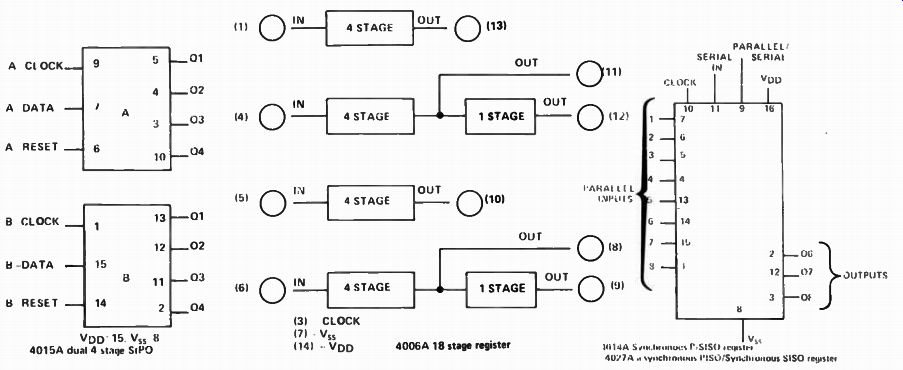
Fig. 1. Pinouts of four small shift registers.
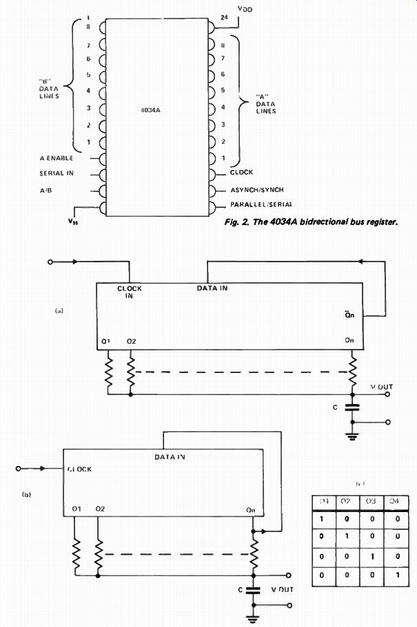
Fig. 2. The 4034A bi-directional bus register.

Fig. 3. (a) Johnson type waveform synthesis (b) principle of the single bit
circulation register (c) counting sequence for (b) when it is correctly set
up.
As far as eight bit data manipulation is concerned, the ultimate shift register must surely be the 4034A whose pinout is given in Fig. 2. It is described as a bi-directional bus register because the two data lines "A" and "B" are interchangeable in that if the A/B input is high the A lines are inputs and the B lines are outputs, whereas when A/B is held low the reverse applies. When the parallel/serial input is high then data is accepted from the parallel inputs (on the positive clock transition when asynch/synch is low, asynchronously otherwise) whereas when parallel/serial is low, data is accepted from the serial input and shifting is performed on the positive clock transition. The only other feature is the A-enable input which enables the A lines when it is high thus allowing several registers to feed a common bus. Designers of large digital processing systems will find many applications of this device.
Applications of shift registers in data storage and conversion are not really very interesting out of context and so we will look briefly at counters. The connection of shift registers ( under the guise of a sequence of flip-flops), to form Johnson counters, has already been considered but it is worth noting that in the same way as we produced digital to analog converters from counters we can also produce waveform synthesizers from Johnson counters (see Fig 3(a)). The calculation of the required value of each register is rather tedious because each is on for half a complete cycle. Nevertheless, an eight stage register gives sixteen separate values out but not all of these are independent. On occasions this method is superior to the single bit approach.
The circuit in Fig. 3(b) is not complete because the single bit must be inserted to start with. If the application will tolerate switches in the starting sequence it is a trivial design exercise but if complete auto-starting is required it becomes quite interesting.
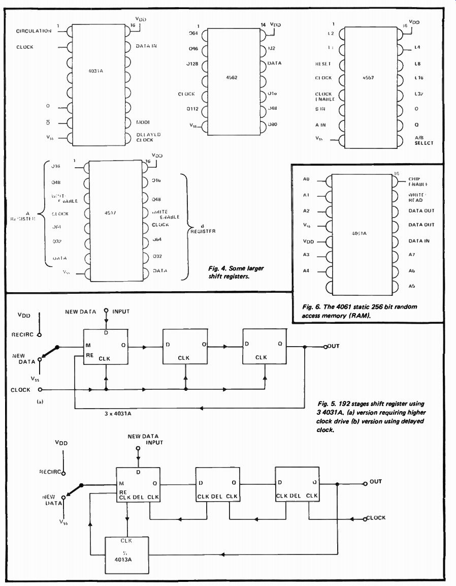
These small registers we have been considering are by no means the top end of the range. Figure 4 gives the pinouts for some high capacity registers.
The 4031A is a single sixty-four stage shift register, the only addition being a Q output and mode and recirculation connections. When the mode control is low, the recirculation input is inoperative and data is accepted from the data input. When mode is high, however, data is accepted from the recirculation input instead. Thus if the Q output is connected to the recirculation input a register is formed with a control input which will either recirculate its contents continually or accept new data, depending on the control signal. You might well wonder why the recirculation input is not internally connected to the Q output.
This is not done because it would generally reduce the versatility of the device and, more particularly, would prevent the formation of multi-chip recirculating registers like the one shown in Fig. 5(a). The 4013A is positive edge triggered and it has also got a delayed clock output which, as the name implies is a replica of the clock signal delayed by several hundred nano-seconds so that the cascading method shown in Fig. 5(b) may be used.
The addition of the flip-flop if recirculation is required should be noted as without it this method will not work.
The cascading method in Fig 5(a) must be used for highest speed operation although it requires higher clock drive.
Having said so much about the 4031A there is less to say about the next three devices. The 4517 is a dual sixty-four bit register, the two devices being distinguished in the pin diagram by the suffices "A" and " B". During normal operation the device is positively edge triggered, data is entered at the data pin and outputs are available at Q16, Q32, Q48 and Q64. This is with the write enable low. When it is high however data is entered at the data Q16, Q32 and Q48 pins ( the Q16 pin acting as a ...
---------- CMOS a practical guide
Fig. 4. Some larger shift registers.
Fig. 5. 192 stages shift register using 3 4031A. (a) version requiring higher clock drive (b) version using delayed clock.

Fig. 6. The 4061 static 256 bit random access memory (RAM).
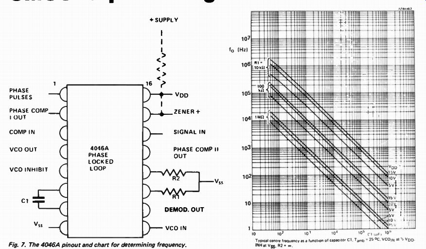
Fig. 7. The 4046A pinout and chart for determining frequency.
... data input to stage 17 etc) thus allowing complete filling of the device in sixteen clock periods.
The 4562 is a straight forward one hundred and twenty eight stage positive edge triggered device with no additions except outputs every sixteen stages throughout.
The 4557 is an altogether more interesting device. Basically, the length of the shift register between the A and B inputs and the Q and Q outputs is equal to the sum of the L inputs which are high plus one. Thus if L32 and L4 are the only ones held high the shift register will be of length 32 + 4 + 1 = 37. The reset input clears all stages to zero when it is taken high. The A/B select input is used to decide whether the A or B inputs will be used as the data source. When it is low B is used, when it is high A is chosen instead.
It should be clear from our previous discussion how a recirculating register could be formed. As for the clocking, when the clock enable is low the device behaves as a conventional positive edge triggered register, but if negative edge operation is required this can be achieved by holding the clock at logical one when a falling edge at the enable input will operate the device. Using this device as a Johnson counter would lead to an interesting binary programmable symmetric frequency divider. Before we leave the subject of shift registers we will point out that all those we have considered are static devices which means that they maintain their state even if they are not clocked for some time. A two hundred stage dynamic shift register is available its type number is 4062A. Of course, a shift register can be used as a memory. The disadvantage is that it is a serial access device which means that a lot of unwanted information must often be passed by while the piece we require is arriving. Random access memories (RAM) avoid this problem because access is by a set of address lines, the signal on which determines which bit of the memory is to be written to or read from.
A typical example is the 4061A two hundred and fifty six bit static RAM. This is simple enough for a brief description of its features to be given easily. AQ to A7 are the eight binary address lines necessary to specify any one bit and these should only be changed while the chip enable input is high. Only when the chip enable has returned to zero can read and write operations be performed - reading when "read/write" is low - writing otherwise. The buffering of the outputs is such that the data in line may be tied to either data out or data out if desired.
It should also be noted that the V_ss and V_DD are unconventionally positioned so that the devices are compatible with other MOS memories.
Of course, there are a few other pieces of timing protocol to be observed. For example, the chip enable signal should not go low too soon after an address change.
THE 4046 A PHASE LOCKED LOOP
The possibilities of combining linear and digital circuitry on the same chip has made the fabrication of the 4046A phase locked loop possible in CMOS. As usual we will discuss this device with reference to its pin diagram, which is given in Fig. 7.
A zener diode of 5.2 V is provided at pin 15 for supply regulation if required although the circuit will operate at any value of VD D between five and 15 volts.
The chip contains two phase comparators with outputs at pins 2 and 13. The first of these is an exclusive - OR network which requires a 1:1 mark space ratio at the input to work effectively, will lock onto harmonics of the input frequency but makes up for a lot by having good noise rejection and it also leaves the voltage controlled oscillator running in mid- range with no input connected. In contrast to this, phase comparator 2 can handle pulses and leaves the oscillator running at minimum frequency. The output from one of these phase comparators is generally connected via a low pass filter to the input of the V.C.O. In passing we will mention that when the first phase comparator is used, the capture range (that is the range of frequencies that will pull the loop into lock) can be made less than the lock range (the range over which the loop will follow an already locked input) by using an appropriate low pass filter. In the case of comparator 2 however, the lock and capture ranges are identical.
The frequency of the VCO for given R1, R2 and C1 is shown in Fig. 7. The highest frequency attainable is over 1 MHz but the supply voltage may need to be a full 15 volts to achieve this with the cheapest plastic encapsulated devices. For experimenting purposes this description of the oscillator is probably sufficient but if it is required to design for specific frequency ranges, the R.C.A. data sheet on the device gives graphs which are easier to use than the somewhat cumbersome formula.
Basically the smaller R2 is, the smaller the range of VCO may be swept over. If pin 12 is left open, the frequency can be swept from a negligible value to a megahertz or over.
If the signal in is within CMOS logic levels ("0"‹ 30% VDD "1" 70% VDD) then it may be directly coupled to the signal input but if capacitive coupling is used signals at least as low as 1.5 V p- p will be accepted. The inhibit input saves power by disenabling the VCO when it is taken high and the "DEMOD OUT" terminal provides a buffered copy of the "VCO IN" signal for use as an output in demodulation set-ups. If this is used a resistor of 10 k- ohm should be connected between it and VSS. Figure 8 shows an FM demodulator designed to operate with a centre frequency of 10 kHz. It uses phase comparator 1 for good noise rejection and the formula for the capture range shows that the values used give ± 400 Hz. As R2 is infinite the circuit will track over a very wide range and the linearity obtainable is very high.
Figure 9 shows the outline design of a frequency synthesizer. The second phase comparator is used because it will deal with non symmetric output from the divider and will not lock onto harmonics. The VCO is set with the pin 12 resistor infinite for maximum range.
Three to nine hundred and ninety nine kilohertz steps can easily be achieved.
The low pass filter should be optimized for minimum settling times. The divide by N counter has been shown as a block as these have been discussed at length previously.
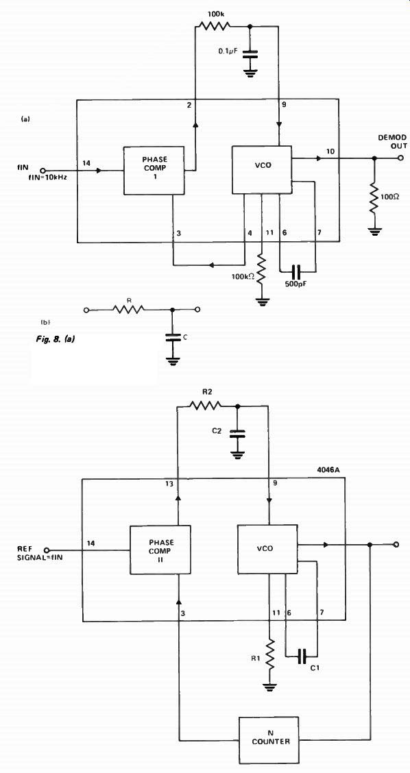
Fig. 8. (al An FM demodulator for 10kHz. (b) Design of low pass filters for
phase comparator 1.
Fig. 9. Basic PLL frequency synthesizer.