Inherently rugged, CMOS logic has many advantages over other logic families - high noise immunity and uncritical power requirements are but two. This, the fourth article in this series, deals with multiplexing.
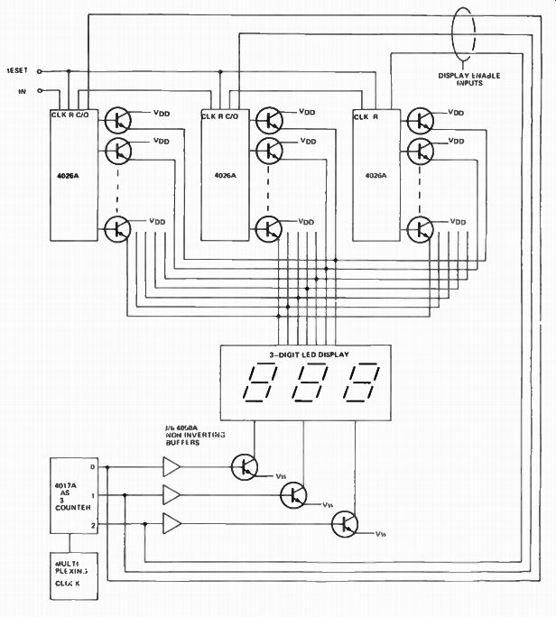
Fig. 1. A three decade counter for a 3-digit multiplexed display. Extra buffering
of the digit lines may be necessary for some displays.
LIFE IS NEVER AS SIMPLE AS WE might want and there are two reasons for complicating the circuitry by using digit multiplexing ( i.e. each digit is displayed for a fixed period, usually between about 10 and 30% of the time). These are that to do so is more efficient in terms of power consumption, and secondly that most multi-digit displays reduce the number of lead-outs ( by giving just one set of seven segment drive lines for the complete display and one digit drive line for each digit). This is the reason why the 4026A has a display enable input which, although the counter continues to function, cuts off the display when it is held low. The display enable output gives a replica of the input and may be used to enable other counters which are to be "on" during the same period. It also explains the presence of the "un-gated C-segment" output which is used for producing some divide by "N" configurations which operate when the display is disabled.
The basic arrangement of a three decade counter is shown in Fig.1 and attention is drawn to the note that additional buffering may be necessary on the digit lines. It is also worth noting the use of a 4017 divide by three counter ( using the flip-flop reset mode) to control the display.
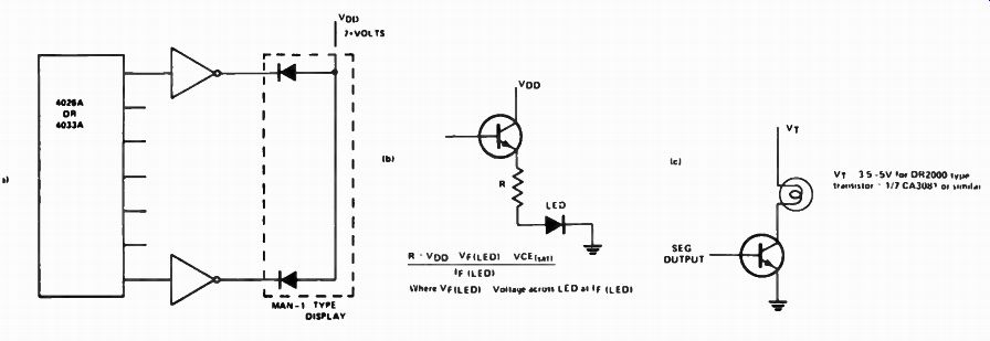
Fig. 2. Driving other displays: (a) MAN- 1 type (b) example of calculation
of limiting resistor (c) Numitron type incandescent display.
Other types of displays which are often used are higher current LEDs such as the MAN- 1 which is, in contrast to the MAN-3 a common anode device.
This means it must be driven by inverting buffers as shown in Fig. 2a We have been relying here on the output current limit of the CMOS chip to limit the forward current in the LEDs. It may be necessary to add current limiting resistors in the segment lines, particularly when transistor drivers are employed. The calculation of the value is simple given the required segment current and voltage drops (see Fig. 2(b). In multiplexed displays the limiting resistors should, of course, be put in the common segment lines. A considerable saving in resistors in non-multiplexed displays may be achieved by putting a single resistor in the common line to each digit. The disadvantage is that the display brightness varies with the digit. Fig. 2(c) shows the technique for inter facing with " Numitron" and similar displays.
The ripple blanking facility is for blanking leading and trailing zeroes in the display and it works as follows.
Take the ripple blanking input ( RBI) of the most significant 4033A on the integer side of the display low. Then take the ripple blanking output ( RBO) of the IC and connect it to the RBI of the next counter and so on until the position of the assumed decimal point is reached. Follow exactly the same procedure from the least significant counter in the fractional part of the display backwards to the decimal point (see Fig. 3(a). Of course, if the assumed decimal point is at one end of the display then half the procedure would be unnecessary. If non- significant zeroes in the places either side of the decimal point are to be displayed ( so that 7 and . 6 appear as 7.0 and 0.6) then the RBIs of the two counters concerned should be taken to Vdd.
Finally on these two ICs, the lamp test facility on the 4033A just forces all segment outputs high when it is taken high.
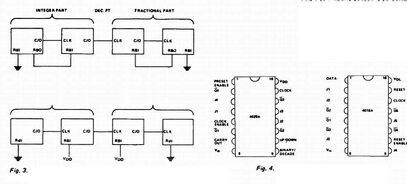
Fig. 3. Four digit counters using the 4033A with non-significant zero suppression
(a) in all positions (b) in first and last position only.

Fig. 4. Pinouts of the 4029A and 4018A.
THE 4029A and 4081A
We shall conclude our discussion of counters by looking briefly at two more devices. The 4029A is a general purpose counter which, at the price that a 7490 was a year or two ago, has most of the features of the more exotic TTL devices. Briefly, the device is positive edge triggered and advances when the clock and preset enables are both low.
Furthermore it counts in binary when the binary/decade input is high and BCD otherwise. A high signal at the up/down input persuades it to count up and a low input forces it to count down.
As though this were not enough, when the preset enable input is high, the Q counter outputs are forced to follow - the J ("Jam") inputs. The prefix "4" in both cases indicates the most significant digit. The pinout diagram is given in Fig. 4 along with that for the 4018A pre settable divide by N counter.
There are two basic ways of producing counters. Firstly there is the chain of flip-flops each of which halves the frequency produced by the one before it. This was the principle behind the binary counters, which we considered at the beginning of this month's discussion, and also of the 4029A. The second method is known as a Johnson counter and it is basically a shift register consisting of a chain of flip-flops with the Q output of the last counter connected back to the data input. A little patience and a pencil and paper will soon show that such a counter will divide the input frequency by 2N where N is the number of stages.
The counting sequence for a four stage counter is shown in Fig. 5 and the reader will notice that if the counter starts with contents not in the counting sequence (e.g. 1010) then the contents are always nonstandard thereafter. Thus some special gating is required. The simplified internal diagram of the 4018A in Fig. 6 is not complete. Also the Jam inputs and preset enable (which work in the same way as in the 4029A) together with the reset ( which zeros all stages ( Q1 - 05 = 1) have been omitted for clarity.
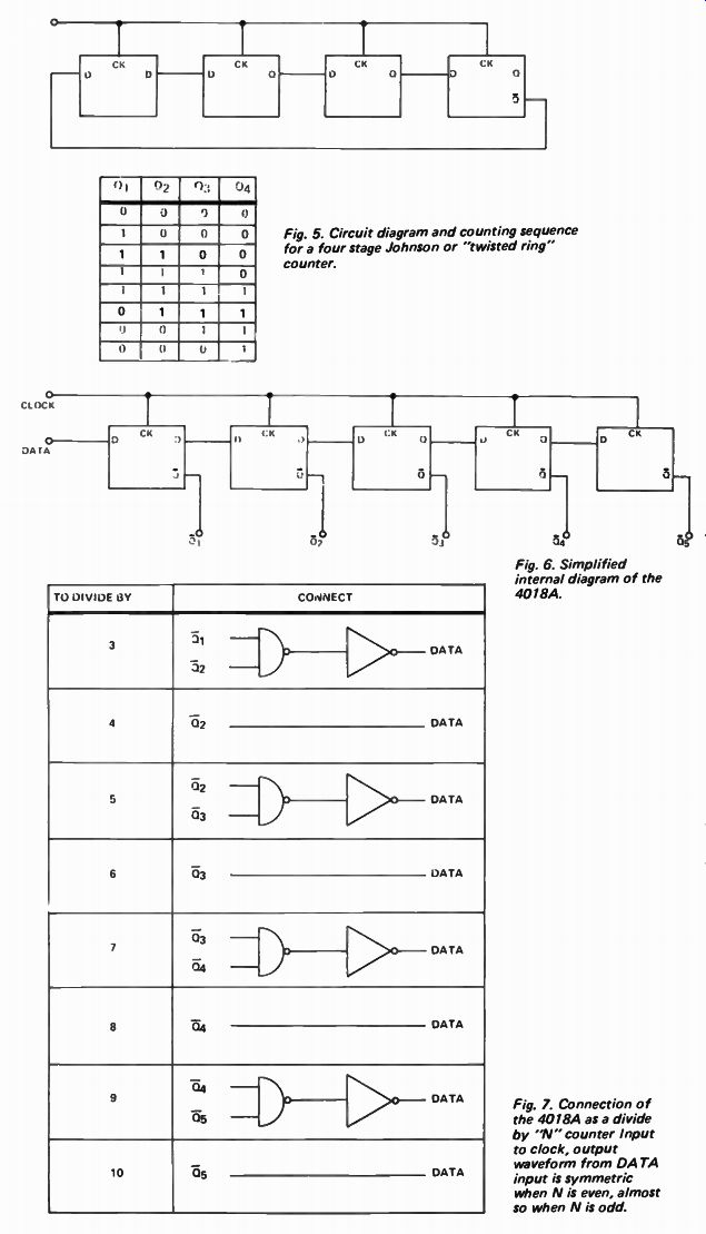
Fig. 5. Circuit diagram and counting sequence for a four stage Johnson or "twisted
ring" counter.
Fig. 6. Simplified internal diagram of the 4018A.
Fig. 7. Connection of the 4018A as a divide by "N" counter Input to clock, output waveform from DATA input is symmetric when N is even, almost so when N is odd.
Figure 7 shows the way to connect the 4018A to divide by all numbers from three to ten. Just as an example of how versatile this device is, one application will be considered in a totally different field from counting. By disregarding the clock, the Jam inputs and inverted data outputs ( d) can be used as a five data latch for temporary storage, the outputs being updated to the inputs while the present enable is high.