T. Bailey completes his series on CMOS.
IN THIS FINAL ARTICLE WE WILL take a brief trip back through several of the topics already covered, looking at some more sophisticated ICs in each group.
The first two devices in Fig. 1 share a common pin-out diagram. They are both dual counters (labeled "A" and "B") with reset operating when high.
The 4518 operates in BCD and the 4520 works in binary. Both devices are capable of counting at at least 2.5 MHz when V_DD = 10 V. The clock and enable inputs are interchangeable in that a positive edge triggered counter may be realised by holding enable at " 1" and using the clock input, or a negative edge triggered device may be obtained by holding the clock high and using the enable input.
The 4553 is altogether a more advanced I.C. It is a three stage decade counter with latches and it provides a multiplexed output. The counters advance on the trailing edge of the clock pulse providing that "disable" is low. It will also advance on the rising edge of a disable pulse if the clock is high. The outputs are multiplexed, which means that one digit is given at a time on the four BCD output lines. The three digit outputs show which digit is being presented ( digit 1 is most significant). The BCD outputs are high when active, the digit-select outputs are low. The multiplexing is driven by an internal oscillator whose frequency is determined by the value of capacitor (1000 pF is about right) connected between pins 3 and 4. Alternatively, this can be overridden by leaving the capacitor out and driving the multiplexing by feeding pulses to pin 4.
The carry out signal may be used to clock succeeding counters and in this case a capacitor may be used to control the multiplexing of the first counter and succeeding ones driven by connecting their pin 4 to pin 3 on the preceding device. The reset input sets all the counters to zero and disables all the digit outputs hence blanking the display when it is taken high. The only other thing to note is the latch enable input.
On the rising edge of the input to this pin the output from the counters is stored in latches and thus the conventional three decade counter ICs and three latch ICs are replaced by a single device. Use of this device is well illustrated by the ETI counter module and also by Fig. 2 which shows a six decade version.
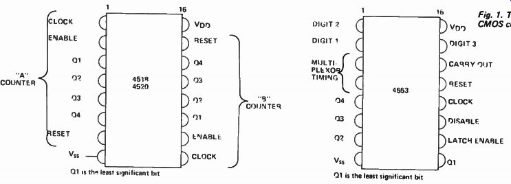
Fig. 1
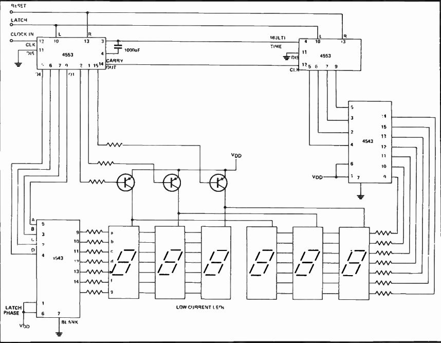
Fig. 2. A six decade counter using CMOS. It may be adapted for common cathode
LEDs by changing the drivers and taking pin 6 on the 4543 s to Vss.
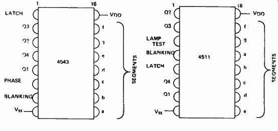
Fig. 3. Two BCD 7 segment decoders and drivers with latches. 01 is the least
significant bit.
The two seven segment decoders used in these two counters - the 4543 and the 4511 - have their pin- out given in Fig. 3. The 4511 is a straightforward device with Q1-Q4 BCD inputs and a-g segment outputs. The three additional connections are simply a lamp test which lights all segments when it is taken low, a blanking input which turns off all segments, when it is taken low (unless lamp test is low as well) and a latch which stores the current input when it is taken high. The segment outputs will source up to 25 mA. The 4543 is more advanced, the latch operates when taken low and the blanking operates when high. The device operates conventionally when the phase input is low ( i.e. is suitable for directly driving common cathode LEDs) but when phase is high, the outputs are all inverted which is useful for driving common anode LEDs. If this input is fed with a square wave which is also fed to the common connection of the segments, liquid crystal displays may be driven in the manner described in part one. The 4056A mentioned there is a pin for pin equivalent of this device except that the blanking is dispensed with and pin seven used as a second V„ pin for the display output part of the circuitry. Thus pin 16 could be at 0 V, pin 8 at - 3 V and pin 7 at - 15 V giving maximum economy while still providing full drive at the output.
There is also a five decade counter of a similar type but there is not space to describe it here. Its type number is 4534 and it comes in a twenty-four pin DIL case.
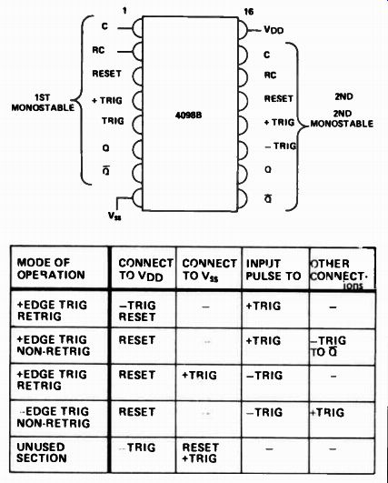
Fig. 4. The 40988 dual monostable multivibrator and method of achieving different
modes of operation.
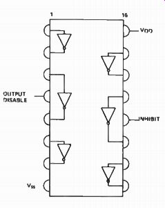
Fig. 5.
MONOSTABLE MULTI VIBRATOR
The 4098B is a dual monostable multivibrator. Its pin diagram (Fig. 4) is accompanied by a table showing the connections needed for every combination of edge triggering and re-trigger-ability. The reset operates when low in this device whose period is, to a first approximation given by T = RC (ohms and farads), where C is connected between the RC and C pins and R is connected from RC to VDD . The specification of the 4528 is similar except for minor details.
MORE GATES
We can now claim to have covered a fair cross-section of devices and so to conclude we shall say a little more on the subject which we started with, simple gates. As well as the NOR and NAND gates we mentioned at the time there is a range of AND, and OR gates available at comparable prices. The 40718, 4075B, 4072B are quad, triple and dual OR gates respectively with identical connections to the NOR gates (4001A, 4025A, 4002A) that were discussed in the first part of this series.
Similarly, the 4081B 40858, 4082B are the AND gates corresponding to the 4011A, 4023A, 4012A we mentioned then.
The 4030A quad exclusive-OR gate was also listed there and it is worth mentioning that types 40708 and 4077 B are exclusive-OR and exclusive-NOR gates with identical pin connections. As the 4070B has slightly superior specification to the 4030A and is usually cheaper it may generally replace it. Also, for almost all purposes the 4507 is equivalent to the 4030A and 4070B. The 4093B is a quad NAND Schmitt trigger with about 0.6 volts hysteresis (at VDD = 5 V) and a pin-out identical to the 4001A. The 4583 is a dual Schmitt trigger in which the hysteresis may be adjusted by external resistors.
There can be few uses for these which have not already been realised with the TTL SN7413N but it is worth noting that larger time constants could be used on the inputs.
Figure 5 shows a hex inverter and buffer with the extra options of an inhibit input which makes all the inverters have low outputs when it is taken high and an output disable which sets all the outputs in a high impedance state. This also operates when it is taken high. The chief use of these circuits is in applying one of two lines of data to an input. They are both wired in but only one disable is low at any one time. The disable overrides the inhibit.
RANGES OF CMOS
Throughout this series, devices have been known by a four digit code number beginning 40 and ending with A or B, or beginning 45 and possessing no suffix. Most of the devices beginning 40 are available from RCA in the CD range with a type number CD40xxAE or CD40xxBE. The A signifies that the maximum supply voltage is 15 V, B signifies 18 V. In general, A and B versions are not both provided. Most of this range is also available from Motorola as thMC140xxCP range which will tolerate up to sixteen volts. The 45 devices are often available only in the MC145xxCP range. In general other combinations of suffices indicate a ceramic packages or the like. Generally these are more expensive and have slightly superior specifications.