Lab Notes-- Safety with CMOS
Certain elementary safety precautions must be taken when handling CMOS ICs or designing CMOS circuits.
Ray Marston explains
EARLY CMOS ICs earned a reputation for being easily damaged by static electricity, either when being handled or when being soldered into circuit boards, etc. Subsequently, manufacturers tried to overcome this 'fragility' problem by providing the ICs with extensive built in input and output protection on each gate in each package. These protection networks do a fairly satisfactory job, but provide the designer with a few extra problems when employing CMOS circuits.
CMOS protection networks cmos ICs are, by definition, metal oxide semiconductor devices, in which the input signal is applied to the near infinite impedance (about 10^12 ohms) of the metal-oxide gate. Typically, the gate oxide has a breakdown voltage of about 80 V; if a gate oxide breakdown does occur, the resultant damage to the device is catastrophic and irreversible.
To protect the CMOS against excessive input voltages (particularly arising from static energy), all modern CMOS VDD ICs are provided with extensive built-in protection on all inputs and outputs.
Figure 1 shows the standard protection network that is used on the vast majority of B-series CMOS devices.
Here, all diodes marked as 'D1' are used to prevent the input or output from swinging more than 600 mV below the Vss (0 V) rail, and all diodes marked as 'D2' are used to prevent the input or output from swinging more than 600 mV above the V_DD ( supply positive) rail. D3 is intended to prevent the V_DD terminal from swinging negative to the Vss pin (electrostatically) when the device is being handled.
There are a couple of minor exceptions to the standard version of the protection network. One of these is the type used on the 4049B and 4050B series of hex buffer/converters which, as shown in Figure 2, have their inputs free to swing well above the VDD rail.
These particular ICs are specifically in tended for use in logic-level conversion applications, in which (for example) the input may come from a 12 V CMOS net VDD work but the output and the IC supply rail are matched to a 5 V TTL network.
Another exception is the 4066B type of transmission gate or bilateral switch, and its equivalents. These devices comprise a bilateral electronic switch and a switch-control network. In these circuits, all switch-control networks have the type of input protection shown in Figure 1, but the switches themselves have the simple protection network shown in Figure 3.
Note in Figures 1-3 that all diodes marked with asterisks are 'parasitic' devices, which just happen to occur fortuitously as an inherent part of the CMOS manufacturing process, while all other diodes are specifically designed into the circuits. Also note that the networks are intended only to give protection against 'normal' electrostatic discharge voltages. When the networks are subjected to ordinary dc signals, the diodes are liable to burn out if their forward currents exceed 10 mA or so, thereby causing possible catastrophic damage to the IC substrate.
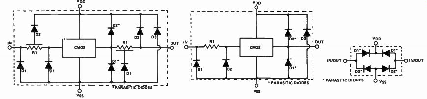
Figure 1. These are the standard electrostatic discharge protection networks
used on most B series CMOS ICs. The two diodes associated with the resistors
are distributed across the entire resistance, as shown.
Figure 2. This protection network is used on the 40498 and 405013 hex buffers. Note that the input is free to swing above the positive supply (V_DD) rail.
Figure 3 The 4066B quad bilateral switch has standard B-series protection on its gate control input terminals, but has this simplified form of protection on its ' switch' elements.
Major CMOS manufacturers such as RCA reckon that an electrostatically charged human body can be approximated by the circuit of Figure 4, in which the 'body' has an effective capacitance of 100 pF and a source resistance of 560R. The manufacturers have carried out extensive tests with this model by charging the 'body' to various ...
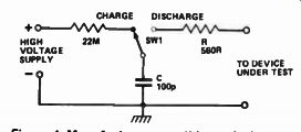
Figure 4 Manufacturers use this equivalent-body discharge network when evaluating
the capabilities of their CMOS protection networks.
... voltages and then discharging it (via the 560R series resistor) into different terminal combinations (input, output, Vss, VDD) of CMOS devices to establish worst-case capability figures for the three types of electrostatic-discharge protection networks. It should be noted in these tests that the 560R series resistor acts as a current-limiting voltage dropper, so the voltage actually reaching the CMOS device is far lower than the initial electrostatic voltage.
The results of the manufacturer's protection capability tests are shown in Figure 5. As you can see, the standard protection network can withstand a 4 kV electrostatic discharge. A quick calculation shows, however, that this represents a peak protection-diode current of several amps, yet we've already seen that these diodes can with stand dc currents of only 10 mA or so.
Puzzled?
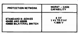
Figure 5 These are the worst-case capabilities of the three different CMOS
protection networks, when tested with the network of Figure 4.
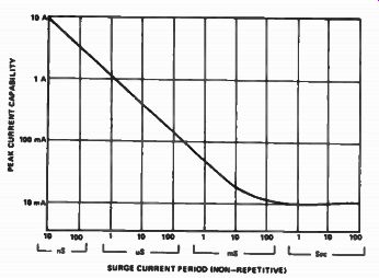
Figure 6. Typical surge-current capabilities of CMOS protection diodes.
Up the junction Just about the only way of destroying a diode is to literally vaporize its junction, and this can only be done by applying an adequate amount of power for sufficient time for the melting process to take place. Since a junction must inevitably be formed on a substrate, which has a finite mass, all junctions inevitably have a certain amount of thermal inertia and are, in fact, destroyed by energy overloads (power-time product), rather than by simple power overloads.
Consequently, it is quite normal to find that a diode rated at 1 A (for example) can, in fact, withstand brief current surges up to several hundred amps. Similarly, CMOS protection diodes, which have very low de current ratings (10 mA), can withstand very high levels of surge current (several amps), provided that the surge current duration is very brief. Figure 6 shows the typical surge current capabilities of these protection diodes. Remembering that the 100p - 560 R 'human body' equivalent circuit has a time constant of a mere 56 nS, it no longer comes as a surprise to note that these diodes can withstand several amps of peak current from a 4 kV discharge! CMOS circuit design By now you will have gathered that you can effectively destroy a CMOS device by simply blowing one or more of its 'protection' diodes with a dc current as low as 10 mA. Consequently, when de signing CMOS circuits, precautions must be taken to ensure that excessive diode current cannot flow in the CMOS chips.
CMOS ICs can be 'blown' by excessive signals applied to either the input or the output terminals. If several CMOS stages are cascaded, empirical experience shows that a front-end 'blow' will usually destroy only a single device (because low energy levels are normally involved), but a rear-end (output) 'blow' will often have a ripple effect (because high energy levels are involved) and cause the destruction of all ICs in the chain.
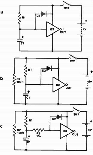
Figure 7. Circuits (a) and (c) are safe, but circuit ( b) will almost certainly
cause front-end blow'. See text for explanation.
The most common cause of front-end 'blow', and its cure, are illustrated in Figure 7. Here, a capacitor is connected directly between the IC gate and the 0 V line; when SW1 is closed, the capacitor charges up via R1 and eventually attains the full positive supply potential. When SW1 is opened (to switch the circuit off), C1 tries to discharge via D2, the 'upper' input protection diode of the gate.
In the Figure 7a circuit, the only discharge path for C1 is via D2 and the IC's supply terminals; consequently the discharge currents will be quite low and the IC will probably suffer no damage.
In Figure 7b, on the other hand, a 100R resistor is connected across the supply terminals, so C1 will try to discharge to ground via D2 and R2, and the resulting 90 mA peak current will almost certainly result in the destruction of the chip.
In practice, R2 may well take the form of various resistors and semiconductor devices distributed throughout the total circuit.
Figure 7c shows the cure for the Figure 7b design problem, a 10k resistor wired in series with the gate to limit the C1 discharge currents to a safe value.
Whenever you design CMOS circuits and have to connect a capacitor between a gate and the 0 V rail, always make sure that the capacitor discharge current is limited to a safe value, either by a series gate resistor or by some other factor.
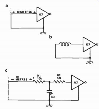
Figure 8. Long input cables, as in ( a), can be equivalent to an inductor (
b), end present another front-end blowing hazard. The cure is simple (c). Figure
8 illustrates another possible cause of front-end 'blowing', and its cure.
In Figure 8a, it seems that the IC's input is safely grounded by the 10 m of
input cable (in practice, this cable may go to a low impedance sensor, etc),
but in actual fact ( Figure 8b) this cable will inevitably be inductive and
can easily pick up unwanted radiation and possibly feed destructive signals
to the IC input. Figure 8c shows that the circuit can be rendered safe with
a simple filter ( R1-C1) and a series gate resistor (R2). Back-end blowing
The most common cause of back-end blowing is unexpected back-EMFs (from inductive
loads) reaching the CMOS output by breaking through from power-driving circuitry.
Inductive loads, such as relays, can generate surprisingly large back EMFs as their fields collapse at switch-off, as can be proved by connecting a relay in the 'buzzer' mode shown in Figure 9.
Typically, a 12 V relay will generate a back-EMF of about 300 V! If you ever use CMOS to switch a relay or other highly inductive load using a transistor driver, always protect the transistor with a pair of 1N4001 diodes connected as shown in Figure 10a. If you want to be really safe, you can use another pair of similarly connected diodes to directly protect the output of the CMOS stage, as shown in Figure 10b.
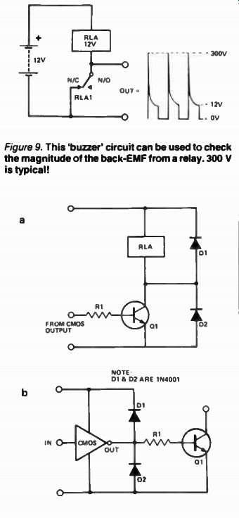
Figure 9. This buzzer circuit can be used to check the magnitude of the back-EMF
from a relay. 300 V is typical!
Figure 10(a). A transistor relay-driver can be protected with a pair of diodes. ( b) The output of a CMOS stage can be given added protection with a similar arrangement.