Wally Parsons looks back to valves to explain VFETs.
A DIODE VALVE emits electrons from a heated cathode and these are then attracted by an electric field to the positive anode. Since only the cathode is heated, current can flow in only one direction. The diode will thus act as a rectifier, conducting only on alternate half-cycles of an AC voltage (see Fig. 1). If a grid structure is placed between these electrodes, it can be used to control current flow. A negative potential will repel electrons, opposing their flow to the anode, and by placing the grid close to the cathode, a small change in grid potential will have the same effect on anode current as a much larger change in anode potential. There fore, the device will amplify. Since the anode current is controlled by the electric field in and around the grid, the triode is, in a sense, a field effect device.
The action is direct, and electron flow responds rapidly to changes in control potential. Moreover, in switching applications it can switch an inductive load rapidly, because the back EMF sees an extremely high impedance and no reverse current flows.
Figure 2 shows the relationship of anode voltage, grid volts, and anode current for a triode. It can be seen that anode current can be controlled by both anode volts and grid volts. If a load is inserted in the anode circuit, current changes will cause voltage changes across the load. These can be plotted in the form of a load line as shown, and also as a transfer curve for the specific load.
The amplification is quite linear, but gain and output are limited -- as shown by the semi-vertical slope of the curves.
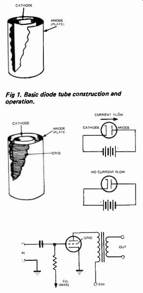
Fig 1. Basic diode tube construction and operation.
Fig 2. Triode construction, circuit and characteristics.
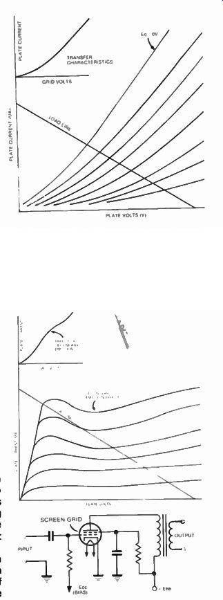
Fig 3. Series output arrangement.
Inserting a second grid between the control grid and anode and applying a fixed positive voltage somewhat lower than on the anode further accelerates electrons, but because of the grid's open structure, most of them continue on to the anode. Note the screen voltage takes precedence over the anode in controlling current. And we can swing the anode voltage further for more output, and get higher gain too.
The addition of the second grid with a fixed high potential results in a current flow essentially independent of anode voltage, but still subject to the action of the control grid. ( Figure 3).
Trouble occurs, however, when we try to produce an anode voltage swing lower than the screen voltage. Electrons are moving so fast that when they strike the anode they dislodge other electrons, which are attracted to the higher potential screen grid, thus reducing current through the load.
This problem was overcome by adding a third grid between the screen and plate and tied to the cathode.
Because it is at cathode potential the grid pushes the secondarily emitted electrons back to the anode, resulting in a family of curves as in Figure 4.
Distributed loading is also possible by dividing the load between screen and anode, and results in Figure 4a. This kind of flexibility makes it possible to design circuits of exceptional linearity.
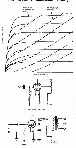
Fig 4. Single ended output with current source.
Problems
So far so good - except for a few problems. To begin with, the valve, like a light bulb, converts more electricity to heat than to useful work. It's very inefficient - for example the author (who is associated with the Canadian version of ETI) uses two 75 watt output class AB valve amplifiers to keep his studio at 25° C. without any additional heating in a Canadian mid-winter! Also like a light bulb, a valve's performance deteriorates from the moment power is applied. Thus, direct coupled circuits can give real headaches in maintaining correct operating characteristics.
And then there's the output transformer. In order to match the thousands of ohms impedance to a low impedance load such as a loudspeaker, a transformer is virtually a necessity. With the inefficiencies already involved we can't afford the resultant impedance mismatches if we try to eliminate transformers. And we can't use gobs of feedback to reduce the resulting distortion. It's bad enough that, if we don't opt for a delicately balanced direct coupled circuit we have a low frequency roll-off and 90° phase shift at every R-C coupling point, but we have in any case the additional phase shift and internal resonances of the trans former. In practice, we are limited to between 20 and 26 dB of overall feed back. Obviously, a high level of open loop linearity must be designed into such an amplifier.
A great deal of engineering energy was spent designing output transformer less amplifiers, but few were successful, and those that were often created more problems than they solved.
Some legendary amplifiers were built using tubes. The Williamson, ( I have one in daily use and it still sounds great), Quad, Leak Point One, Macintosh Unity Coupled. The Quad, for example, delivered all of 15 watts - and was rock stable driving an electrostatic ( Quad, of course) at live performance levels. Mac's drove a lot of disc cutters ( at 60 watts) to produce discs which still sound spectacular.
But many were anxious to do some thing with the new-fangled transistors, and we did.
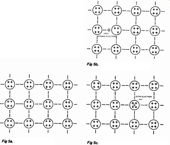
Fig 5a. Basic lattice structure
Fig 5b. P-type lattice structure.
Fig 5c. N-type lattice structure.
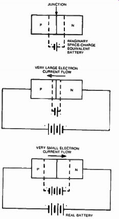
Fig 6. Drain to source resistance against temperature (Siliconix).
Transistors
The bi-polar transistor is composed of three materials, either a p-type semi conductor between two n-types, or an n-type between two p-types, ( Figure 7a). A semiconductor such as silicon or germanium has a crystalline structure in the form of a diamond lattice with each atom having four adjacent neighbors, held together by covalent bonds, each bond involving a shared pair of electrons. These electrons are not avail able for conducting current, so conduction is very semi. Indeed, resistance being around 100 million times that of copper.
However, if we introduce an impurity such as phosphorus or arsenic which has five valency electrons four of which form bonds while the fifth is only lightly held and is available for conduction. This is an n-type material (negative as it has an excess of electrons). If we add an impurity such as aluminum, only three valence electrons are available. Therefore, one of the valence bonds is not completed, resulting in a vacancy or hole in the lattice structure ( Fig. 5). An electron from an adjacent electron pair bond may absorb enough energy to break its bond and fill the hold. This is a p-type material.
This doesn't look like much of a big deal, but the result is quite dramatic.
Note that the atomic structure is in equilibrium - there is no net charge. However, if a free electron breaks its bond, it leaves behind a positive net charge; if it completes a bond by entering a hole, a negative net charge results.
Current flow is produced by bringing about this carrier mobility. What was originally a very high resistance is now, under the right conditions, able to conduct substantial current, just as a small impurity (e.g. sulphuric acid) added to non-conductive pure water, makes electrolytic conduction possible.
When p and n-type materials are joined together, a p-n junction is formed (Fig. 6). Some of the free electrons from the n-type material diffuse across the junction and recombine with holes of the p-type material. The opposite process takes place with holes from the p-type material, producing a space charge or depletion region on either side of the junction, giving the p-type material a slight negative charge, and the n-type a slight positive charge. This process is finally limited by the resulting potential gradient.
If a battery is connected, as shown in Figure 6a, free electrons from the n-type material are attracted to the positive terminal, while holes from the p-type material are attracted to the negative terminal, widening the space charge region and increasing the potential gradient until it approaches that of the external battery. There is now little or no voltage difference across each region and little or no current flow. The junction is reverse biased.
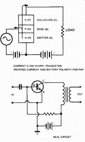
Fig 7a. Current flow in a semiconductor and circuit diagram.
If we reverse these polarities ( Fig. 6b) electrons in the p-type material break their bond and enter the battery creating new holes, while electrons from the battery negative terminal enter the n-type material and diffuse toward the junction. The space charge region narrows and the energy barrier becomes insignificant, so that excess electrons from the n-type material can penetrate the junction and move via the p-type holes to the positive battery terminal, for as long as voltage is applied.
The junction is now forward biased.
Work!
In the device shown in Figure 7, the forward-biased emitter-junction injects electrons into the base region. The impurity or doping levels chosen are such that almost all the emitter current is composed of these electrons, and very few holes are injected into the emitter.
The base region is very thin so that nearly all injected electrons diffuse to the edge of the depletion region of the reverse-biased base-collector junction where the field sweeps them across the collector bulk. Since for an equal current more power is developed across a high resistance than a low resistance, amplification occurs as a result of current being transferred from the low resistance emitter-base junction to the high resistance collector junction.
The curves show that, as with the pentode tube, current is controlled mostly by the control electrode ( base), but in this case the controlling parameter is current, not voltage. We have an inherently low- impedance device, and since it requires current into its input impedance, its signal source must be capable of delivering power. An ideal transistor requires input current, unlike an ideal vacuum tube. This reduces efficiency but we don't have to heat up a cathode to shake a few electrons loose, so our overall efficiency is vastly greater.
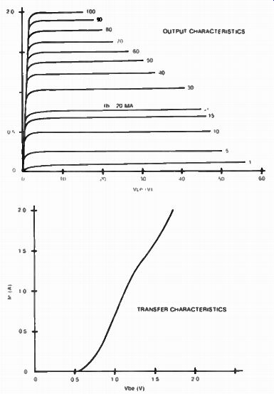
Fig 7b. Output and transfer characteristics of the 2N3054.
Disadvantage
The major disadvantage of this type of device lies in the nature of the depletion layers at the junctions, particularly the emitter-base. When current flows in a transistor, excess charge is stored in the base region. If the base emitter junction is changed from a forward to reverse bias state, as in the negative swing of a class B or AB stage, or when a class A stage is overdriven, the junction cannot immediately switch to the reverse blocking state due to the presence of these excess charge carriers.
They have the effect of allowing current to flow in reverse as if forward biased, until these charge carriers are removed.
In addition, there is capacitance effect associated with the barriers of a reverse-discharge time. The result is a switching transient during part of a cycle, sometimes erroneously referred to as crossover distortion (the latter occurs in any device in push-pull and is due to a discontinuity in the transfer function, usually caused by incorrect bias). This can be reduced by reducing the junction area but this reduces the dissipation capability. In fact, a transistor design favoring one characteristic usually does so at the expense of others.
Also, as temperature rises in the device (due to current flow, for example) carrier mobility at the junctions increases, causing further increase in current. The current increase further raises temperature, which raises current-- which further raises temperature - and so on. The resulting thermal runaway can quickly destroy the device.
In milliseconds! In large area transistors, current tends to become nonuniform in distribution. The temperature rise in the high current region leads to localized thermal runaway until equilibrium is reached by a sharp drop in collector voltage, ( called secondary breakdown) frequently destroying the device. This is more true at high voltage and low current than the reverse, and frequently means that rated dissipation cannot be reached. This leads to overdesign, unnecessarily high voltage and dissipation ratings (and remember, a design which favors one characteristic often does so at the expense of others) plus elaborate protective circuits.
High levels of feedback are generally used to control distortion, and this in conjunction with the excess charge condition in the base, leads directly to transient overload, and resultant transient intermodulation. Output is delayed during this charge/discharge, which delays application of feedback. It simply isn't available. The input signal is not immediately reduced by feedback, and passes through at high initial level.
The millennium has not quite arrived after all! The FET Since a semi-conductor is precisely that, a battery connected across the ends of a p- type or an n-type bar will cause current to flow through the material, just as it does through a vacuum tube.
We discussed earlier the characteristics of a pn junction. If, for example, a p-type material is joined to the surface of an n-type bar, located between the battery terminals, a pn junction is formed, and if this junction is reverse biased, a space charge or field is produced of opposite polarity which will inhibit current flow, just as the control grid inhibits current flow in a vacuum tube.
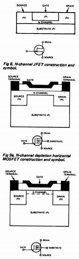
Fig 8-9a. N-channel enhancement horizontal MOSFET construction and symbol.
Changing this reverse voltage causes a large current change, and amplification results.
A simple junction FET is shown in Figure 8. With a given drain-source voltage, maximum current flows at zero gate voltage, and at some reverse voltage, determined by device geometry and doping levels, no current will flow. Also, as in the vacuum tube, load characteristics are not reflected to the input circuit, because current is not controlled by carrier injection as in bipolars, but by voltage levels.
A variation is the Metal Oxide Semi conductor Field Effect Transistor.
(MOSFET) ( Fig. 9) a far more versatile device whose technology is virtually the cornerstone of modern computer technology, although it has had less use to date in linear applications such as audio amplification.
MOSFETS come in two basic types.
In both the gate consists of a metal electrode separated from the channel by a thin oxide layer. In the depletion type current flow is controlled by the electrostatic field of the gate when biased. When a depletion MOSFET is so biased the device may be driven on both sides of the zero volts point as with vacuum tubes. Unlike vacuum tubes, under these conditions, the gate draws no current, therefore does not require the driver to deliver power.
The enhancement type MOSFET shown in Figure 9b, is more widely used. The source and drain are separated by a substrate of opposite material, and under zero gate volts no current flows.
However, when sufficient forward bias is applied to the gate the region under the gate changes to its opposite type (e.g. p-type becomes n-type) and provides a conductive channel between drain and source. Carrier level, and conduction is controlled by the magnitude of gate voltage.
Although MOSFETS are handy devices they are not capable of handling high power levels. The channel depth available for conduction is limited by the practical limits on gate voltage. The lower current density has been the primary limitation due to the horizontal current flow.
VFETS
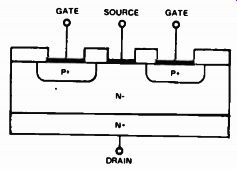
Fig 10. Vertical junction FET construction.
Recent years have seen the introduction and commercial use of Vertical Channel J-FETS, notably by Sony and Yamaha (Fig. 10). The vertical channel permits a very high width-length ratio, permitting a decreased inherent channel resistance and high current density. Unfortunately it suffers the same disadvantages as the small signal J-FET, plus, in currently available devices, a very high input capacitance, ranging from 700 pF to around 3000 pF, limiting high frequency response. In addition, since they must be biased into the off condition, bias must be applied before supply voltage and removed after the supply if it is to be operated anywhere near its maximum ratings. This problem doesn't exist with vacuum tubes because of heater warm-up time, although some "instant-on" circuits impose heavy turn on surges.
This necessitates a complex power supply, and Yamaha, for example, uses more devices in the supply than it does in its amplifier circuits. However, the construction does make possible the design of complementary types and both Nippon Electric and Sony have high power devices available. Unfortunately, neither company seems anxious to make detailed information available, so there is little to disclose here beyond the fact that they are said to have characteristics similar to those of triode tubes.
However, the Vertical MOSFETS by Siliconix are readily available, at reason able prices, and the manufacturer most generous in providing data. The following information is extracted from their application note AN76-3, Design Aid DA 76-1, plus device data sheets.
The Device
Notice in Figure 11, that the substrate and body are opposite type materials separated by an epi layer (similar to high speed bi-polars). The purpose of this structure is to absorb the depletion region from the drain- body junction thus increasing the drain-source break down voltage. An alternative would have involved an unacceptable trade-off between increasing the substrate-body depth to increase breakdown voltage (but increasing current path resistance)
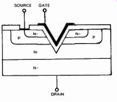
Fig 11. Vertical MOSFET construction and lengthening the channel. In addition,
feedback capacitance is reduced by having the gate overlap n-epi material instead
of n+.
In manufacture, the substrate-drain and epi layer are grown, then the p-body and n+ source diffused into the epi-layer, in a similar manner as the base and emitter of a diffusion type transistor. A V groove is etched through the device and into the epi-layer, an oxide layer grown, then etched away to provide for the source contact and an aluminum gate deposited. This type of device allows current flow in one direction only; this is not always so with a similar type of horizontal FET, where source and drain may be identical in structure and of the same material.
Therefore, no reverse current flows (we hope) when used in switching applications, as was also the case with vacuum tubes.
In-circuit operation is refreshingly simple: Supply voltage is applied between source and drain, with the drain positive with respect to the source, under which conditions no current flows, and the device is off. This is an enhancement type device, and is turned on by taking the gate positive with respect to the source and body.
The electric field induces an ohm channel on both surfaces of the body facing the gate, and allows electrons to flow from the negative source through the induced channel and epi and through the substrate-drain. The magnitude of current flow is controlled almost entirely by the gate voltage, as seen in the family of curves ( Fig. 12) with no change resulting from supply voltage changes above 10 V. Advantages The vertical structure results in several advantages over horizontal MOSFETS.
1) Since diffusion depths are controllable to close tolerances, channel length, which is determined by diffusion depth, is precisely controlled. Thus, width/ length ratio of the channel, which deter mines current density, can be made quite large. For example, the VMP1 channel length of about 1.5µ, as against a minimum of 5 µ in horizontal MOSFETS, due to the lower degree of control of the shadow masking and etching techniques used in such devices.
2) In effect, two parallel devices are formed, with a channel on either side of the V groove, thus doubling current density.
3) Drain metal runs are not required when the substrate forms the drain contact, resulting in reduced chip area, and thus reduced saturation resistance.
4) High current density results in low chip capacitance. Also, unlike horizontal MOSFETS, there is no need to provide ...
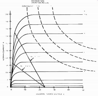
Fig 12a. Output characteristics VMP1.
Fig 12b. Other VMP1 characteristics.
... extra drain gate overlap to allow for shadow mask inaccuracies, so feedback capacitance is minimized.
In comparison with bi-polars, especially power devices, the advantages are even more impressive.
1) Input impedance is very high, comparable to vacuum tubes, since it is a voltage controlled device, with no base circuit drawing current from the driver stage. A 7 V swing at the gate, at virtually 0A, represents almost 0W of power, but can produce a swing of 1.8 A in output current. This represents considerable power gain and will inter face directly with high impedance voltage drivers.
2) There is no minority carrier storage time, no injection, extraction, recombination of carriers, resulting in very fast switching and no switching transient in class B and AB amplifiers. Switching time for a VMP1 is 4 ns for 1 A, easily 10-200 times faster than bi-polars, and rivaling many vacuum tubes.
3) No secondary breakdown, and no thermal runaway. VMOS devices exhibit a negative temperature coefficient with respect to current, since there is no carrier recombination activity to be speeded up with temperature. Thus, as current increases so does temperature, but the temperature rise reduces current flow. It is still possible to destroy the device by exceeding its maximum ratings, but a brief near-overload does not result in an uncontrollable runaway condition.
Usually, simple fusing and/or thermistor protection is sufficient for maximum safety, and even this may be unnecessary with conservative design. Absence of secondary breakdown means that full dissipation can be realized even at higher supply voltages. In this respect they resemble vacuum tubes.