In the first part of this article we examined the structure and features of a new type of semi-conductor, the vertical channel power metal oxide semi-conductor field effect transistor, Vertical MOS-FET, or V-MOS recently introduced by Siliconix. The second part of the article covers the actual use of V-MOS. V-MOS POWER FETS like signal MOS-FETS, may be used to perform many different functions. However, no matter what the circuit, certain conditions, common to all applications, must be provided. These are supply power, loading, drive signal, and establishment of appropriate operating points.
The electrical characteristics of the VMP1, VMP11, and VMP12, are shown in Fig. 1, and Fig. 2 shows them in graphic form. Since these are uni-directional devices, the source and drain are not interchangeable, and as they are n-channel devices conduction can occur only if the drain is positive with respect to the source, and high enough to ensure operation in the linear region - as with a vacuum tube, bi-polar transistor, or signal FET. Like the vacuum tube, the absence of secondary breakdown allows full dissipation at any voltage supply up to maximum voltage and current ratings.
Thus, where two different designs require the same dissipation but different voltage/load current, no derating is required. This is shown in the "safe operating area" curves. The only bi-polar transistor possessing this characteristic is the single-diffused type, which is also the least suitable for any application requiring wide bandwidth and/or high speed.
This characteristic also simplifies the establishment of suitable load- lines allowing greater safety margin in driving reactive loads where the load-line may be elliptical to the point of leaving the safe-operating area. Designers accustomed to using high voltage high dissipation devices to assure adequate safety margins at relatively low power levels need not therefore be too disconcerted at the 25 watt rating of these devices.
A 10 watt class A amplifier suitable for driving a tweeter in a bi-amped speaker system, for example, need not suffer excessive dissipation except per haps with an electrostatic unit where such a power level would be inadequate anyway, unless it were operating at a very high cross-over frequency.
Output
These devices may use any of the types of output circuits in general use with tubes and bi-polars, including transformer coupled ( Fig. 12) where the benefits of the absence of charge carrier storage become apparent in the absence of severe ringing at the cross over point, conventional series output such as in Fig. 3, which is a straight forward transformation from a bi-polar...
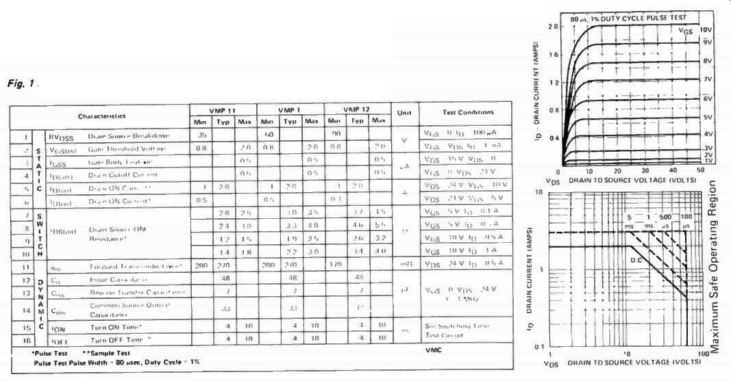
Fig. 1 Electrical characteristics of the VMP devices ( Siliconix)

Fig. 2 Typical VMP1 performance curves
... circuit ( 1), and single-ended output with current source, also transposed from an excellent bi-polar circuit ( 2) (Fig. 4).
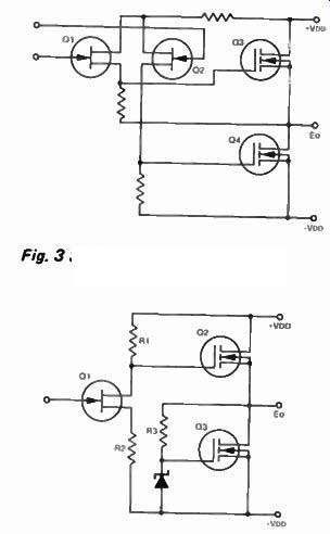
Fig. 3 Series output arrangement.
Fig. 4 Single ended output with current source.
Bias and Drive
These series of devices are n-channel, enhancement type MOSFETS, and may be biased and driven using methods appropriate to signal types and bi-polars.
The drain is made positive with respect to the source and the gate enables conduction by being forward biased with respect to the source, that is to say it is biased in a positive direction. Unlike bi-polars, however, they are voltage, rather than current controlled, and circuit values are selected to provide the required voltage. Any current drawn is by the bias network itself.
Three bias methods are shown in Fig. 5. Figure 5a shows bias supplied from a fixed bias supply. It is the simplest possible method, allows extremely high input impedances since Rg may be almost any very high value desired, and its stability is limited only by the stability of the bias supply.
The design shown in Fig. 5b has the advantage of requiring no extra supply voltage since it is taken from Vdd.
Disadvantages are low impedance and stability. Input impedance consists of the parallel combination of R1 and R2 (disregarding input capacitance of the MOSFET and the very low input leak age.) There are practical limits as to how high this combination can become; if for example, we have a 60 volt supply and require 6 volts bias, we might have some difficulty obtaining higher values than 9 megohms and one megohm for R1 and R2.
Higher values become more difficult to obtain, stability becomes less reliable, internal inductance and distributed capacitance become problems, and over coming these difficulties usually costs money. In addition, if Vdd is subject to variation, then bias varies. In a class AB amplifier this could be quite serious, since Vdd varies considerably with output level; at high levels, Vdd can be expected to drop, causing a reduction in bias.
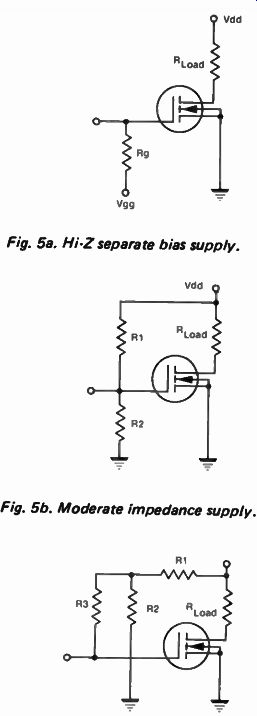
Fig. 5a. Hi-Z separate bias supply. Fig. 5b. Moderate impedance supply. Fig.
5c. Hi-Z common supply.
While this may reduce the danger of over-driving the device, it will be forced to operate in its non-linear region which may result in unacceptable performance characteristics unless taken into consideration in the overall circuit design (e.g. choice of feedback values). It does provide some degree of overload protection, and with correct choice of values can provide for class AB operation at low levels, shifting to class B at high levels. With these considerations in mind, and/or where moderate impedances are required, it offers a low cost, simple, and reasonably reliable method of establishing the operating point.
The method used in Fig. 5c is similar except that with the addition of R3 higher input impedances are possible.
Its configuration is similar to a noise less biasing system frequently used in low-level bi-polar amplifiers and integrated circuits (e.g. National LM381A) but its function is somewhat different.
Resistors R1 and R2 form a voltage divider as in Fig. 5b, but their junction now forms a fixed bias source as in Fig. 5a. Resistor R3 can be quite high since no current flows. Meanwhile, since the parallel combination of R1 and R2 are effectively in series with R3 they can be reduced to more manageable values.
Alternatively R2 can be replaced by Zener diode for stability comparable to Fig. 5a.
Input Protection
Unlike most signal MOSFETS, the gate of each of these devices, with the exception of the VMP4, is protected with an internal 15 volt, 10 mA zener diode. Most signal MOSFETS, as well as the VMP 4, are unprotected, or where extremely high impedances are not required, are protected by back to back zeners. I have no information as to why this different technique is used.
This different technique is used, but it is obvious that a negative signal swing on the gate will result in forward current through the zener. If the device is to be driven beyond cutoff, the driver must be capable of delivering current during its negative swing. Alternatively, a constant current source can be used, a series limiting resistor or a driver biased to the same class of operation as the V-MOS FET. A constant current source (we'll examine an example of its use a little later) will limit current drive to the value of the constant current diode used; a series resistance will drop the drive voltage as the diode draws current.
In both cases, diode current must be limited to 10 ma maximum. Higher currents will damage the protective zener diode.
In amplifier applications, a class A driver is commonly used. However, if a class B output is used, conduction only occurs during positive half-cycles. There fore drive signal is not required during negative half-cycles. If a source or emitter follower driver stage is biased so as to pass no negative drive, the problem does not occur. However, great care must be exercised in the design of such a stage to ensure that drive does not disappear before the output device is cut off.
This is not too difficult with a class B or near class B stage; If the output device is operated at zero bias, then a small amount of bias on the driver will ensure conduction during slightly more than 180 degrees. Class AB operation is a little more tricky. If conduction is to occur for 270 degrees, for example, the driver should conduct for slightly more than this period.
Two types of drive circuits familiar to designers of bi-polar circuits are the Darlington and super beta, commonly used together to provide a quasi-complementary circuit. Both circuits are current amplifiers designed to provide a compound device with very high hfe and provide base current to the output device. However, similar circuits can be used with these devices to provide phase inversion in a series output stage.
Thermal considerations
As described earlier ( Part 1) these devices exhibit a negative temperature coefficient with respect to current, so that as temperature rises, current is reduced, thus providing a self- inhibiting action which provides some protection against overload. However, this is not an unconditional effect Fig. 6 shows the relationship between RDS(on) and temperature ( 3), based on a worst case temperature coefficient of 0.7 percent per degree C. Suppose that the device when 'on' passes a current of 1 amp which causes it to heat up. The 'on' resistance increases (which is why current drops), increasing the voltage drop across the device and the device dissipation. Now, if adequate heat sinking is used there is no real problem but if it isn't, the ' on' resistance and junction temperature will rise to the point where extra charge carriers are generated, thus stabilizing
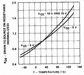
Fig. 6 Drain to source resistance against temperature (Siliconix).
RDS(on). That's great, except for the fact that this doesn't occur until the maximum safe junction temperature of 150 degrees has been exceeded.
You'll remember that we said earlier that the device was free of thermal runaway problems because of its negative temperature coefficient, but it isn't free of thermal destruction problems, and in any case, excessive temperatures will reduce output conductance. Heat-sinking requirements are, therefore, similar to those of bi-polars. The calculations of thermal operating conditions are beyond the scope of this article, but interested readers are referred to the Siliconix literature listed in the references, ( 4). Extending the ratings The current handling and therefore total dissipation capability may be increased by simply connecting several devices in parallel ( Fig. 7). No ballast resistors are needed to ensure proper current sharing since if one device draws more current than another it simply gets a little warmer which causes it to draw less (assuming adequate heat sinking, of ...
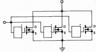
Fig. 7 Basic circuit for parallel operation course). The only major precaution
needed is to keep lead inductance in the gate and source connections to a minimum to prevent parasitic oscillations, unless the devices are driven from a
low impedance source.
It may be advisable to insert what the British call " stoppers" - small resistors ( 100 to 1000 ohms) in series with each gate, wired directly to the socket, or ferrite beads mounted on the leads close to the socket terminals. An additional plus when paralleling several devices is that the gm is multiplied by the number of devices used. Mutual conductance gm is specified as the ratio of a large change in current to a small change in control voltage. If, for example, a change of 0.4 volts on the gate produces a change of 0.1 amp through one device, connecting two devices in parallel will give us an output swing of 0.2 amps, but it will still require only the original 0.4.100 V
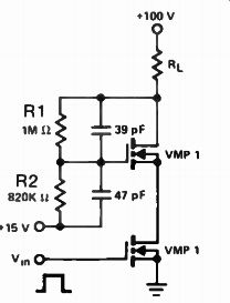
Fig. 8 Diagram
for series operation (Siliconix ). volts gate swing. Since voltage gain A=gm
x RL, if gm is increased, A is increased.
In real use, of course, the internal resistance of two devices in parallel is less than of one, the optimum load is less, so in amplifier applications, the net amplification A is the same. But notice that the drive requirements have not changed. With bi-polars current would have to be supplied to each base, thus increasing the output requirements of the drivers. Indeed, with many high power amplifiers using multiple output devices the drivers are also power devices.
We can also extend the voltage ratings by series operation of two or more devices Fig. 8 shows the technique. Resistors R1 and R2 bias Q2 'on' while C1 and C2 ensure fast switching. The input control signal is inserted between gate and source of Ql.
Ordinarily the bottom of the divider chain is at ground potential for signal frequencies, so that circuit is really a cascade.
Maximum current and gm are the same for one device.
Some practical applications
An efficient light dimmer circuit as proposed by Siliconix is shown in Fig. 9.
The 4011 acts as a pulse width modulated oscillator whose duty cycle is determined by the ratio of R1 to R2, with R2 adjusted to control the bright ness of the W-90 bulb. Of special interest here is the fact that with its fast switching time, the VMP1 is especially suited to pulse width modulation at power levels and suggests it as being suitable for use in switching, or class D linear amplifiers.
A DC to DC converter is outlined in Fig. 10. The VMP1s form an oscillator with positive feedback provided by the additional coil in the gate circuits.
In operation the upper V-MOSFET is biased 'on', and the lower V-MOSFET
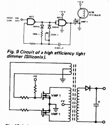
Fig. 9 Circuit of a high efficiency light dimmer (Siliconix).
Fig. 10 A d.c. to dc. converter (Siliconix). is 'off'. When power is applied the upper device conducts causing current to flow from Vdd through the upper half of the transformer primary and the upper V-MOSFET to ground. The induced current flow through the feed back coil develops a voltage such as to shift the bias in the upper device 'off' (if the winding is connected with the correct polarity) and the lower device 'on'. This causes current flow from Vdd through the lower half of the trans former primary and the lower V-MOSFET to ground.
The secondary circuit consists of a single rectifier and filter. The resistor in the upper gate prevents shorting out gate bias, and the one in the lower gate keeps both sides balanced. In addition, each resistor limits current through the protective diodes. These are expensive devices for such an application, but the high reliability, the reduced rf radiation (due to reduced switching transients) and the circuit simplicity easily make up for the cost. The very high circuit impedance enables running frequency to be set by the self- resonance of the transformer.
Single-ended push-pull transformer coupled audio amplifiers are shown in Figs. 11 and 12. Both utilize the biasing system described in Fig. 5b. A load line drawn on the output characteristic will show the optimum load to be 24 ohms. In Fig. 11 gate drive is supplied by a single junction FET, and voltage feedback is taken from the output transformer secondary and series fed to the source of the input device. Distortion is under 2% at full output (try to get that with a single ended tube or bi-polar) and could probably be reduced even further by adopting a source follower output stage.
A push-pull version of Fig. 11 is shown in Fig. 12 using a differential input to provide phase splitting, drive, and a feedback point. Although the transformer winding ratio implies the use of a low impedance loudspeaker, a step-up ratio could be used for direct coupling to art electrostatic speaker, a balanced transmission line ( both with some modification of the feedback circuit) an unbalanced transmission line, or a 70 volt speaker distribution line.
Notice in both circuits, and in the biasing circuits of Fig. 5, that no source resistors have been used, either for local feedback or for bias setting. In tube and bi-polar circuits it's a useful technique, and with bi-polars can be used to stabilize bias and control thermal runaway by using the increased current flow to increase the voltage drop, thus reducing base-emitter voltage. However, if used with these devices, it will actually impair the self-limiting action of its negative temperature co-efficient. If temperature rises due to high current, current flow is reduced. This would reduce the voltage drop across a source resistor, lowering the source voltage and increasing the gate-to-source voltage, causing an increase in current flow. The circuit would work great while it lasted -- which wouldn't be for long.
Record amp
Figure 13 shows a magnetic recording amplifier derived from a tube circuit.
Its biggest advantage lies in its ability to provide equalization for head losses by incorporating the head within the feedback loop. Additional equalization is then required only for gap losses and tape self-demagnetization. Q1 acts as a driver for (12, the output stage, which, with series resistor R9, provides a high impedance current source for the record head, as well as providing a mixing pad between audio and bias currents.
The record head's return path to ground is through R11. The inductance of the record head results in an impedance characteristic which rises with frequency. At frequencies at which the impedance of the head is low in comparison with R9 and R10 in series, load current is essentially constant. As frequency rises, however, head impedance becomes appreciable. With appropriate selection of R9 and All, depending on head characteristics, the voltage across R11 decreases as the head impedance becomes significant. If feedback is taken across R11 it will decrease with rising frequency, causing an increase in gain, at a rate of 6dB/octave.
Feedback is applied across R3 via R10 and C8 (which supplies bass boost below 80 Hz) C5 and C6 provide additional high frequency boost for a total ultimate slope of 12 dB/octave.
This circuit is so effective that no additional boost is needed at 15 ips, and only a small amount at 7.5 ips with high coercivity tape.
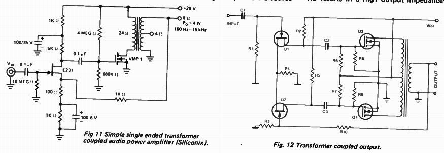
Fig. 11 Simple single ended transformer coupled audio power amplifier (Siliconix).
Fig. 12 Transformer coupled output.
The biasing method used is that of Fig. 5c. The large amount of local current feedback provided by R2 and R3 results in a high output impedance ...
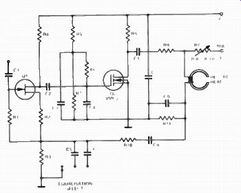
Fig. 13 Tape recording amplifier.
... for Q1, so the biasing network is selected to provide high impedance with reasonable values. Capacitors C3, C4, C7 and C9 bypass bias signal to avoid overloading Q2, and to prevent attenuation of bias current.
Power amp
Figure 14 shows a high quality power amplifier designed by Siliconix Inc. (5) and described in their application notes. Output current capability is increased by using three VMP12's in parallel, providing for 6 amp current 75 watt dissipation and load optimized at 8 ohms. Q11-13 operate as a source follower, while Q8-10 form a quasi source follower. This is accomplished by applying local feedback from drain to gate via R14, R15, and driving the gate by a modified current source. This consists of a cascade circuit with E constant current diode as the load.
For the benefit of those not familiar with these devices, a constant current diode is really a FET connected internally as shown in Fig. 15. Since current in a FET is controlled essentially by the gate-to-source voltage, changes in load or in applied drain-to-source voltage have negligible effect since gate-to-source voltage is held constant. This is a current analog to the zener diode and is described in detail in Siliconix literature ( 6).
The design is push-pull from input to output, thanks to differential circuitry throughout, prior to the drivers. Open loop distortion is low, bandwidth wide, allowing satisfactory performance with only 22 dB of feedback. Lead compensation only is used (via C4), along with the liberal use of local feedback ( R4, R5, R11, R12,). The result is very low transient IM and a slew rate of over 100 V/microsecond. THD is quite respect able even though the numbers might not impress the average audiophile accustomed to amplifiers with great specs and poor sound.
Incidentally, D8 and D9 illustrate an excellent method of providing output current limiting. In this case, 9.1 volt zener diodes limit drain current to slightly less than 2 amps. At first one might be tempted to depend on the built-in protection diodes to accomplish this, but it should be remembered that these devices are for protection against static discharge. Their zener voltage of 15 volts at 10 mA cannot possibly be used since the absolute maximum permissible drain current occurs at a gate-to source voltage of 10 volts.
Commercial amps
A simplified version of Yamaha's B1 amplifier is shown in Fig. 16, (8). In this circuit a cascade drive system is used, but in a differential form with the constant current source in the ...
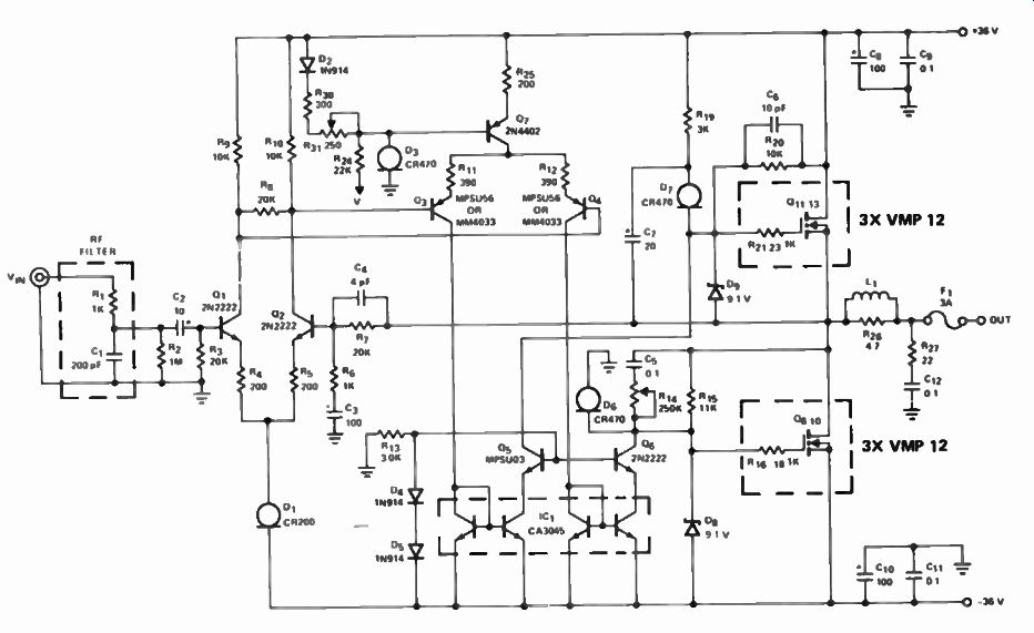
Fig. 14 A high quality 40W amplifier (Silicon ix).
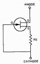
Fig. 15 A FET as a constant current diode.
... common source circuit. This is an example of all FET design of excellent performance and received rave reviews in several publications including ETI. It's also inexpensive! The VHF linear amplifier in Fig. 17 will deliver 5 watts peak envelope with second and third order intermodulation at - 30 dB from 144-146 MHz.
It will also prove useful as a receiver pre-amp with a noise figure of 2.4 dB. V-MOSFETS show considerable promise in rf applications because of their linear transfer characteristic, the high gain capabilities even with Ft somewhat above 600 MHz, low noise and ( in receiver front ends) very wide dynamic range. Although this article has dwelt on the VMP 1 family, there is also the VMP 4, designed specifically for rf applications and which is now available.
Finally, how about something elegant for its simplicity, such as the tapered current voltage limiting battery charger shown in Fig. 18. This is especially useful with Ni - Cad batteries which are intended for stand-by use and are permanently on charge, such as electronic clocks. Overnight shut-downs of a few hours are occasionally but irregularly experienced. You know what this can do to clocks. Especially alarm clocks which are supposed to make noises, turn on radios, start the coffee at a pre-set time in the morning so you can go to work. Battery operation is not too satisfactory if the readout is on continuously, and Ni - Cads should not be on permanent floating charge.
With this little device current is supplied to the battery via the VMP-1.
Gate voltage is set at a value equal to the desired end-of-charge voltage. As the battery charges, its voltage increases, reducing gate-to-source voltage, thus reducing charging current. When the battery reaches full charge its voltage, and that of the source, equals gate voltage, and charge is terminated. If a load is placed across the battery it will draw current, and as the battery voltage drops slightly below gate voltage, charging at a trickle rate occurs - automatically.
Experimentation
The various applications shown are intended as suggestions for further experimentation. They are mainly designed to illustrate various characteristics of the device under consideration, and are not necessarily representative of commercial practice or of finished designs. In some cases this may be just as well! But we would be delighted to hear of any readers' experience with any of these or other circuits.
The author's feeling is that V-MOS constitutes a genuine breakthrough in semi-conductor technology, as import ant as the silicon transistor and the FET itself. We'll be seeing more of these devices, with higher ratings ( a 10 amp 200 volt unit is already under development) and specialized characteristics.
They are said already to be in use commercially as magnetic core drivers.
Digital enthusiasts may be somewhat impatient with the strong emphasis on audio applications in this piece but other literature has placed great emphasis on digital applications, with little attention paid to linear techniques beyond the 40 watt amplifier described here.
The serious reader in all areas is referred to the references at the end.
Further literature may be obtained from Siliconix Inc., 2201 Laurelwood Rd., Santa Clara, CA 95054. They have been most helpful in providing information for the preparation of this article.
Have fun.
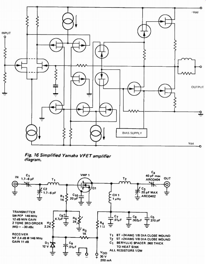
Fig. 16. Simplified Yamaha VFET amplifier diagram.
Fig. 17. 144-146 MHz linear amplifier
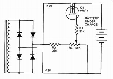
Fig. 18. Tapered current voltage limited battery charger.
REFERENCES
1. W. Marshall Leach: " Construct a Wide Bandwidth Preamplifier" Audio, Feb. 1977, p.39.
2. Nelson Pas: " Build a Class A Amplifier" Audio, Feb. 1977, P. 29.
3, 4. Lee Shaeffer: " VMOS-A Breakthrough in Power MOSFET Technology" Application Note AN76-3, May 1976, Siliconix Inc.
5. Lee Shaeffer: "The MOS-POWER-FET Audio Amplifier" Design Aid DA76-1, May 1976, Siliconix Inc.
6. "The FET Constant Current Source" Design Idea D171-1, January 1976. Siliconix Inc. Also Siliconix Field Effect Transistors Data Book.
7. Ref. 5,
8. Bascom H. King: " Power FETs" Audio, Feb. 1975, p. 42.
10. Ed Oxner. "A New Technology: Application of MOSPOWER FETs For High Frequency Communications" Technical Article TA76-2, Nov. 1976, Siliconix Inc.