by Brian Dance
IN 1976 Siliconix startled the semi conductor world with a new type of power MOSFET device. Recently other manufacturers have produced many other types of MOSFET products which are challenging power transistors and Darlingtons.
The name MOSFET stands for Metal Oxide Silicon Field Effect Transistor.
Field effect transistors (FETs) are essentially voltage controlled devices, unlike conventional transistors in which the small base current controls a larger collector output current. FETs have very high input impedances so that very little input current is required to control their output current.
The input impedance of MOSFETs is especially high because they have an insulating film of silicon dioxide between the input gate electrode and the channel through which the output current flows. The gate electrode is therefore essentially completely insulated and virtually no input current can flow.
Various types of small MOSFET devices have been available for many years. Internally they contain a very small silicon chip on the surface of which the MOSFET device has been fabricated. Any current passes through these devices in a horizontal direction through the very thin surface layers and therefore the maximum current is quite low; maximum power dissipation in such devices is not normally over 1W. VMOS devices In the so-called VMOS devices, developed by Siliconix about four years ago, the current flows vertically through the semiconductor material -- hence the name VMOS. This name is also associated with the V-shaped groove formed in the surface of the semiconductor material of such devices.
Figure 1 shows a cross-section of a VMOS transistor.
If the gate electrode is connected to the source and the drain contact at the bottom of Figure 1 is made positive relative to the source, no appreciable current will flow from drain to source, since the internal diode formed between the p and ohm type materials will be re verse biased. If, however, the gate electrode is made positive with respect to the source, the electric field produced by the gate potential creates a channel in the position shown in Figure 1. A current can now flow upwards from the drain through the channel to the source.
As the gate becomes more positive, the width of the channel increases and the current from drain to source increases.
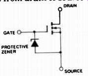
Figure 2. Zener protection of the gate.
If small changes in the gate voltage are to produce the required channel depth, the insulating layer must be extremely thin, which results in an appreciable gate input capacitance (typically some 50 pf). The thin layer also imposes a limit to the maximum voltage which can safely be applied to the gate without the risk of breaking down this thin layer and thus destroying the device. As the gate input resistance is so high (often of the order of a million megohms), it is very easy for small stray electrostatic charges to be picked up on the gate and produce voltages which can puncture the insulating film.
------------
DRAIN CONTACT
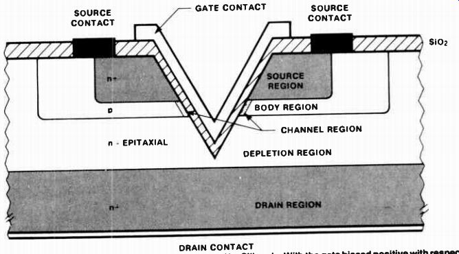
Figure 1.
Structure of the VMOS device developed by Siliconix. With the gate biased positive with respect to the source, current flows from the drain region to the source via the channel region indicated. As the gate is biased more positive, the channel region increases, increasing the drain- source current. VMOS FETs are majority-carrier devices and can switch current in less than 10 ns. Bipolar transistors cannot compete as they suffer from minority carrier storage in the base region.
---------
DRAIN
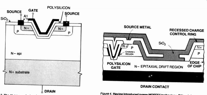
Figure 3. The U-groove device, introduced by Intersil,
reduces problems associated with the intense electric field at the edge
of the V-notch in VMOS devices. The polysilicon layer prevents migration of
sodium impurity ions through the gate oxide layer, a source of chip failure
in VMOS.
DRAIN CONTACT

Figure 4. Having introduced power MOSFET technology, Siliconix have gone on
to improve the devices. The tri- planar construction shown here allows much
higher packing densities on the chip, the smaller size resulting in lower on
state resistance. Polysilicon gates are buried in the oxide layers allowing
source metallization to cover a greater fraction of the chip area •
In some devices a small zener diode is connected between the gate and the source, as shown in Figure 2. If the gate to source voltage exceeds the zener voltage, the zener conducts and shorts out the voltage, protecting the MOSFET. However, the maximum zener current is quite small, so the zener can easily be damaged. The maximum input voltage 'in circuit' should not exceed the zener voltage so that the zener is used to provide protection against electrostatic charges only.
If the gate becomes more than a fraction of a volt negative with respect to the source, the zener will conduct in its for ward direction. If one wishes to operate a MOSFET with the gate voltage negative with respect to the source at any part of the duty cycle, a device not containing a zener should be selected, but then one must take precautions to avoid electrostatic charge pick up.
The first VMOS devices marketed were n-channel devices, with an n-type channel formed in the p-type material shown in Figure 1. Siliconix still only market n-channel devices, but some other manufacturers offer both p channel and n-channel types.
Comparison with bipolars
As the early VMOS devices could not handle so much current or so much applied voltage as conventional transistors, yet were more expensive than the latter, they obviously had some ad vantages or their manufacture would not have been a viable proposition.
Ordinary bipolar transistors suffer from the disadvantage of minority carrier storage in the base region.
VMOS products are majority carrier devices and can therefore switch a current in less than 10 nanoseconds and operate up to several hundred mega Hertz. For example, the 2N6657 can switch 1 A on or off in less than 4 ns, this being 10 to 200 times faster than a comparable bipolar device.
'Secondary breakdown' is another problem with bipolar transistors. If the current density increases at one point, the temperature rises in this region, leading to a still greater current density-- a positive feedback effect which can lead to the rapid destruction of the device. In VMOS devices, an increase in the current density in the channel produces an increased temperature which results in a lower current density in that region, so that the current density automatically equalizes itself throughout the chip without the formation of hot spots.
It follows that it is possible to connect two or more VMOS devices in parallel (often without any additional components), since the total current is automatically shared equally between the devices. Any device passing more current than the mean will become hotter and this will reduce the current somewhat in that device.
Apart from their higher cost, one of the disadvantages of VMOS devices is that their saturation voltage (typically 2V, maximum 4V for some devices when passing 1A) is much greater than for bipolar transistors. Although the V shaped groove utilizes the silicon area quite efficiently, the relatively sharp bottom of the groove is a disadvantage, since a strong electric field can be developed at this point between the gate and the drain where the insulating layer tends to be thinner than else where. This results in a limited operating voltage capability owing to the possibility of gate to channel breakdown.
A perfect switching device would have an infinite resistance in the off state, but the drain current of many VMOS devices is in the nA region when in the off state with gate and source voltages equal. The resistance in the conducting state is normally a few ohms instead of the zero resistance of the perfect switch. This on-resistance is greater for devices with higher voltage ratings.
U-groove devices
The problem of the relatively intense electric field at the edge of the V-shaped notch of VMOS devices has already been mentioned. Intersil, followed by some other manufacturers, reduced this problem by producing devices with the structure shown in Figure 3, where the bottom of the groove is flat. Note that there is an additional layer of phosphorus-doped polycrystalline silicon between the gate and the insulating layer of silicon dioxide. This overcomes another problem of the early VMOS devices, namely the migration of sodium impurity ions through the gate oxide layer, which can cause reliability problems.
Other VMOS products In 1980 Siliconix announced an improved tri-planar VMOS process with the device structure shown in Figure 4.
The source, the gate and the drain are each fabricated in a different plane. It is stated that this type of structure allows much higher packing densities on the chip and the smaller size will enable lower on state resistances to be obtained. Polysilicon gates are buried under the oxide layers so that the source metallization can cover a greater fraction of the chip area.
Another major improvement from the tri-planar structure arises from the use of thin low-resistivity doped layers and from a re-arrangement of the V grooves for optimum use of the epitaxial layers.
Vertical DMOS
Although the modified VMOS processes are very good for devices rated up to about 150 V, they are not ideal for higher voltages. The vertical DMOS structure shown in Figure 5 has been found very suitable for high voltage devices. The current flows upwards from the drain into the n-epitaxial layer, but then flows horizontally for a short distance through a channel to the source.
Supertex of California use this technique to make devices with ratings of up to about 500 V, but somewhat higher voltage devices of this type are likely to become available. Figure 5 shows how the main junction region is surrounded by a concentric second junction which is in turn surrounded by a third junction.
Apart from high voltage capability, this process can produce devices with a very low on-resistance (down to 0.05 ohm). In addition the devices are very fast, owing to the low gate capacitance. For example, a 1A device can' operate at about 2 GHz and a 10 A device at about 500 MHz.
The Ferranti Company of Oldham, England have co-operated with Supertex to develop vertical DMOS devices, both n-channel and p-channel, with ratings up to 650 V and drain currents up to 16 A continuous.
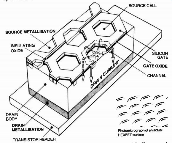
Figure 7 Construction of the HEXFET device introduced by the International
Rectifier company in mid- 1980. The hexagonal source cells ( hence the name)
are connected by a common silicon gate.
Claimed advantages include high voltage and current ratings plus very low on-resistance.
Figure 5. In the vertical DMOS device, current flows from the drain ( N +) into the n-epitaxial layer ( N - ) then flows horizontally through a channel into the source. The concentric rings of p-type material around the main junction help improve the current capability and reduce the on- resistance. This form of construction achieves significantly higher voltage and current ratings compared to prior power MOSFETs.
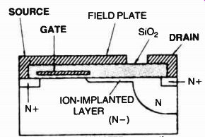
Figure 6. Hitachi MOSFET construction.
Hitachi devices
Hitachi has developed a MOSFET device with the structure shown in Figure 6. The gate oxide layer is designed to handle only 20 to 30 V, so a field plate is provided to prevent high electric fields from forming near the gate. This type of device is most suitable for audio frequencies and for operation at up to a maximum of a few MHz. Both p-channel and n-channel types are available with ratings of up to 200 V and 8A.
HEXFET devices
In mid-1980 International Rectifier introduced a range of devices named HEXFET after the hexagonal structure of the source cells which are connected by a common silicon gate ( see Figure 7). The density of these source cells is over half a million per square inch.
HEXFET devices are available in both p-channel and n-channel polarities and can handle high power levels. They have voltage ratings of up to 500 V and continuous current ratings of up to 25 A. Values of channel resistance as low as 0.05 ohm can be obtained in the on state.
Some of the main applications for HEXFETS include servo motor control, RF induction heating, welding control equipment, audio amplification and other uses where the control of high power is required.
--------- Vos - DRAIN TO SOURCE VOLTAGE (VOLTS) DRAIN - SOURCE VOLTAGE, Typical Transfer Characteristic For 100V. IRF150 HEXFET - The saturation characteristics of a VMOS device ( left) and a HEXFET ( right)
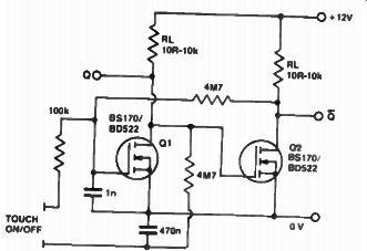
Figure 10. Capacitive touch switch will cycle on and off if finger is held
on the sensor.
SIPMOS
The latest technology to emerge in the power MOSFET field is SIPMOS from Siemens of West Germany, which is an extension of the vertical DMOS technique. Siemens have used this technique to fabricate the first 1000 V MOSFET device, the BUZ 54, which can handle 5 A. It is expected to have wide uses in switching mode power supplies.
Other SIPMOS devices have ratings in the range of 50 V to 500 V, all being n-channel types. SIPMOS transistors can switch loads of up to 5 kW using inputs to the gate of less than 1 mA at 5 V. Maximum drain currents of up to 30 A can be handled, while on resistance values can be as low as 0.03 ohm.
Applications
Power MOSFET devices can be used as alternatives to power transistors and power Darlington devices in many applications, but they are generally more expensive than the latter and the circuit designer must decide which types of device are most suitable for his own application.
The use of power MOSFET products is particularly attractive when one can take advantage of their high switching speed or their high frequency capability. Although they may be somewhat more expensive than other transistors, the use of these new devices may simplify circuitry and reduce the overall costs.
For example, a conventional power transistor requires a considerable current at its input and one or more driver stages may be required to provide this current, whereas the high input impedance of the power MOSFET enables the latter to operate with such small input currents that power driver stages can usually be eliminated.
4.12V
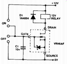
Figure 8. Simple touch switch.
Simple touch switch The circuit of Figure 8 shows how the very high input impedance of a VMOS power MOSFET can be employed in a simple touch switch. When the circuit is first switched on, the capacitor C1 is normally fully discharged, so the VN46AF VMOS device passes negligible drain current.
When the upper pair of contacts is touched, current flows from the + 12 V line ,through the person's skin and charges C1. The VN46AF device is thus biased to conduction and the relay closes. If a finger is now placed across the lower touch contacts, C1 discharges and the VN46AF is turned off; opening the relay. The diode Dl is used to bypass the transient voltages formed when the current ceases to flow through the relay coil - such voltages can destroy
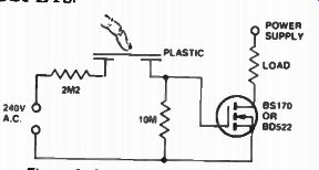
Figure 9. Capacitive touch switch.
Capacitive touch switch
The gate circuit impedance of VMOS devices is so high that circuits can be designed as touch switches in which no part of the circuit is actually touched. In Figure 9 (designed by ITT Semiconductors), the presence of a finger just above the plastic material at the point of separation of the electrodes under the plastic is sufficient to cause current to flow in the load.
The capacitance between each of the electrodes and the finger allows a small alternating current to flow through the 2M2 safety resistor to the gate circuit of the small BS170 or the larger BD522 n-channel device.
Figure 10 shows another touch switch designed by ITT Semiconductors, only a single touch point being used for on/off operation. When power is first switched on, T1 will conduct and T2 is kept non-conducting. Touching the sensor contacts will cause T2 to conduct and feedback from the drain of this device through the 4M7 resistor to the gate of T1 will keep the latter device in the non-conducting state. The 470 uF capacitor now becomes charged.
If the sensor is touched again, the positive potential from this capacitor is transferred to the gate of Ti and the latter device is switched to conduction, whilst T2 is turned off. If the sensor is touched for longer than about one second, the circuit will operate as a relaxation oscillator which changes its state about once per second. The load impedances employed in this circuit need not be identical, any values from about 10 ohm to 10k being suitable.
CMOS Interfacing
The 4000 series of CMOS logic devices can provide only small output currents, but sometimes one wishes to use the output from such a device to control a relay or other load which requires a relatively large current. A VMOS device can conveniently be employed to match the high output impedance of a CMOS device to a relatively low load impedance such as a tungsten filament lamp.
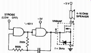
Figure 11. Audio alarm.
An example is the audio alarm circuit f Figure 11. Two of the four logic gates f a CD4011 device are connected as a standard 2 kHz oscillator. Any appreciable current taken from the output of his oscillator affects the operation of he circuit, but the VN66AF requires negligible current and forms an ideal interface device between the CMOS oscillator and the loudspeaker.
When the upper input of the left hand CMOS gate is connected to the + 5 V line, oscillation takes place, but when this input is connected to ground, oscillation ceases. Thus a high impedance logic output can be used to switch the oscillator on and off through the use of this input to the left hand gate.
Figure 12 is an interesting variation of the circuit of Figure 11 in which the four gates of a 4011 device are used to form two oscillators. The two left hand gates form a sub-audio frequency oscillator which modulates the audio oscillator formed by the two right hand gates of Figure 12. Thus one obtains a much more impressive two-tone alarm sound than with the simpler constant note circuit of Figure 11.
The timer circuit of Figure 13 is another example of VMOS interfacing between a CMOS device and a relay. In the quiescent state, the upper input to the left hand gate will be low and the output from this gate high. Thus the output from the right hand gate will be low and the relay will remain open.
If the start switch is momentarily closed, the high input applied to one in put of the left hand gate will cause the output from this gate to go low, while the output from the right hand gate goes high and switches the VN46AF to conduction. Thus the relay closes.
The capacitor between the two gates charges slowly through the fixed and variable resistor from the positive supply line. When the inputs to the right hand gate become sufficiently high in potential, the output of this gate goes low and by feedback to the left hand gate the circuit switches back rapidly to its quiescent state in which negligible current passes through the relay. The length of time for which the relay remains closed can be set by the 1M pot or by altering the value of the capacitor connected between the two gates. When the values shown are used, times obtained range from a few seconds to a few minutes as the variable resistor is moved.
Delay switch
A simple VMOS delay switch is shown in Figure 14. When the switch is closed for a moment, the capacitor becomes fully charged and the VN46AF passes current through the load. The capacitor slowly discharges through the 10M resistor, so the gate voltage of the VN46AF will eventually fall to a value where very little current can pass through the load.
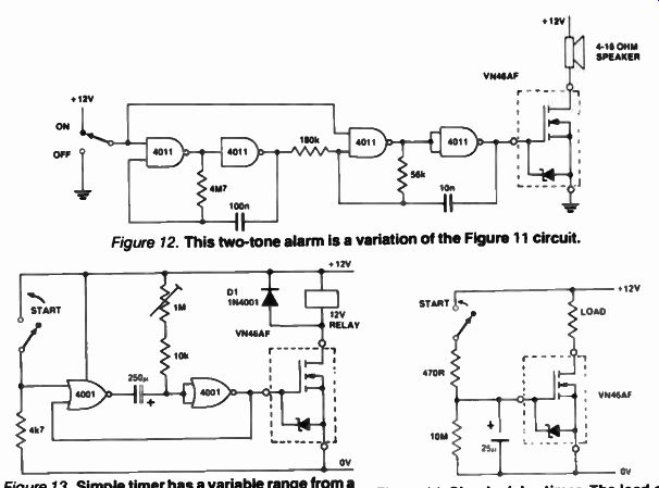
Figure 12. This two-tone alarm is a variation of the Figure 11 circuit.
Figure 13. Simple timer has a variable range from a few seconds to a few minutes. The 1M pot sets the time the relay holds in. Figure 14. Simple delay timer. The load could be a lamp, relay or whatever.
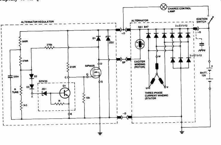
Figure 15. The latest power MOSFET development, SIPMOS, has already found application in automotive electronics. This circuit is an alternator regulator and employs a SIPMOS device rated at 500 V/8 A and an on resistance not greater than 0.2 ohm.
Auto applications The fast switching ability of MOSFET devices renders them very suitable for use in vehicle electronic ignition systems. Timing pulses from a magnetic or other contactless pickup may be fed to an IC which provides a voltage output for the control of a MOSFET device. The latter switches the current through an ignition coil to provide the required high voltage.
An automobile circuit using a SIPMOS transistor as a power switch is shown in Figure 15. As in so many applications of MOSFET devices, the high input impedance of the SIPMOS device is utilized here, since it can be voltage driven by a suitable IC. This circuit is for an automobile alternator voltage regulator and has been de signed for a SIPMOS device rated at ...
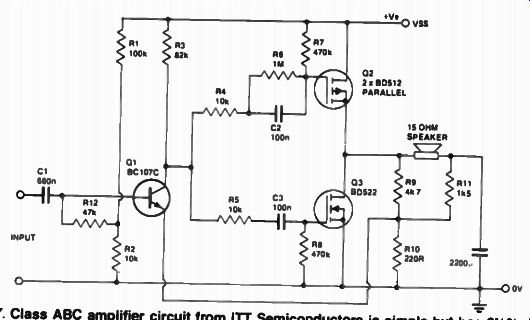
Figure 17 Class ABC amplifier circuit from In Semiconductors is simple but
ha; 3 , /z% distortion at 1.75 W and is only suited to general applications.
... about 500 V maximum drain-to-source voltage, 8A current and an on resistance of not more than 0.2 ohm.
Simple audio applications
The excellent linearity of VMOS devices has attracted considerable interest in their possible use in the audio field but the relatively high price of these devices and their previously limited power handling capability retarded their adoption until recently.
They may be used in simple, low-power circuits, but moderately high power ultra-low distortion circuits have also been designed using VMOS devices.
The very fast switching ability of VMOS devices also makes them very suitable for Class D pulse width modulation circuits.
To operate a VMOS device as a simple class A amplifier, it is only necessary to provide a bias network so that the device operates in its linear region without cutoff. The gate is connected to a tap on a resistive potential divider across the power supply lines and the input signal is capacitively coupled to the gate. The gain will be approximately equal to the mutual conductance of the device multiplied by the load resistance; gain values of over 30 dB are obtainable, and this gain extends well into the MHz region.
A circuit of this general type is shown in Figure 16. The bias level of the Au0n, INFui
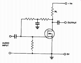
Figure 16 General circuit of a simple class-A audio amplifier using a power
MOSFET. VMOS device is stabilized by means of negative voltage feedback from
the drain to the gate circuit.
Figure 17 shows a particularly interesting circuit from ITT Semiconductors which they call a class ABC amplifier, since it is basically a Class B amplifier, but one of the transistors is more in Class A, while the other is definitely in Class C. It is a simple circuit not designed for particularly low distortion.
The output stage is unusual in that it comprises two BD512 p-channel VMOS devices in one part and a complementary BD522 single device in the other part. This is because hole mobility in the p-channel BD512 is only half that of the electron mobility in the n-channel BD522s so two p-channel devices are required to obtain about the same mutual conductance as that provided by the single n-channel device. As explained earlier, MOSFETs can be connected in parallel without extra circuitry because they automatically share the current.
As the drain electrodes of the VMOS devices in Figure 17 are connected to the device tabs, all of the tabs can be bolted to the same heatsink without the need for insulating washers. The negative feedback circuit compensates for any variations in the biasing requirements of the particular VMOS devices employed. Both ac and dc feedback are employed, but there is heavier dc feed back through R11 and R10 to stabilize the quiescent dc output voltage at half the supply potential so as to ensure a maximum available output voltage swing.
This circuit provides a voltage gain of 30 and a bandwidth extending from 35 Hz to 125 kHz at the - 6 dB points.
Distortion increases at ultrasonic frequencies above about 25 kHz (as with most audio amplifiers). When a 25 V supply is used, the distortion is a minimum of about 0.4% at about 0.5 W, rising to about 0.8% at 1 W, 2% at 1.5 W and 3 1/2% at 1.75 W.
High fidelity
In 1976 Siliconix published a circuit for a high quality 40 W amplifier using VMOS devices, but each half of the output stage required three VMP12 (now designated 2N6658), 90 V TO-3 devices in parallel. Thus, twelve of the devices were required in a stereo amplifier providing 40 W per channel. Rather cumbersome - and costly. However, distortion at the mid-frequency range was only about 0.04% at the 40 W level and about 0.025% at the 1 W level. Only 22 dB of feedback was needed to obtain a response flat to 4 MHz and the slew rate was 100V/ps! One of the advantages claimed for VMOS amplifiers is the lack of transient intermodulation (TIM), because the power bandwidth exceeds the small signal bandwidth. For any frequency below 500 kHz, the amplifier simply overloads before TIM appears.
Taking things a step further, the circuit in Figure 18 is a simple power amplifier first published in the Hitachi MOSFET application notes. The 2SK133 and 2SJ48 have an on resistance of roughly two ohms, so that at 7 A peak output current you can expect a voltage drop of about 14 V across each device. With the power supply voltages shown the circuit is capable of around 50 W. Transistors Q1 and Q2 form an input differential pair that compares the in put signal with the output signal of the amplifier. The difference between these two signal voltages is fed to a second differential pair, Q4 and Q5. This ensures that the open-loop voltage gain of the amplifier is high and allows a fairly high feedback factor when negative feedback is applied. A relatively large amount of negative feedback is essential when using MOSFETs like this in audio amplifiers to linearize the MOSFET characteristics which have, on average, 10 times the distortion of a typical bipolar transistor of similar power capabilities.
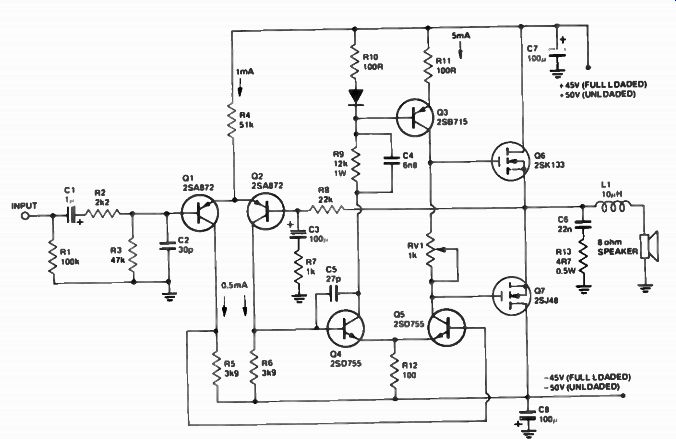
Figure 18. Circuit of a 50 W hi-fi amplifier from the Hitachi MOSFET application
notes. Performance is quite good but dependent on the driver transistors.
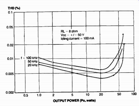
Figure 19. Distortion characters of the circuit in Figure 10.
The transistors forming the driver stage, Q3 and Q5, have been specially designed by Hitachi to drive MOSFETs.
They're superb devices, having a Vce of 100 V and a typical gain (hFE) of around 500. With these transistors the distortion characteristics shown in Figure 19 can be expected. Unfortunately, these transistors are not available in Australia at the present time and substituting alternative available transistors degrades performance considerably. A BD139/BD140 complementary pair for instance, with typical hFE of around 50, is not capable of pro viding the necessary open-loop gain, especially at high frequencies. An experimental circuit we built with BC177s and BD139/BD140s gave less than 0.02% at 1 kHz at full power, rising to as much as 0.1% or more at 20 kHz. So, MOSFETs with all of their advantages have disadvantages too - mainly due to the fact that the forward transconductance is only a fraction of that of a good bipolar transistor.
In order to design an extremely high quality amplifier employing MOS FETs, we are really faced with a new set of problems to solve, but with the promise of performance that makes it worthwhile. (This section on Figure 18 inserted by David Tilbrook ... Ed.).