Lab Notes---Don't go off about Schmitt triggers look at the 4093! This highly versatile package can be used in a wide variety of applications, including: wave- shaping, timing, logic circuits and waveform generation. Ray Marston explains.
ONE OF THE HANDIEST 'building blocks' in electronic circuitry is the Schmitt trigger - a simple circuit block whose output changes state when the input goes above or below a certain "threshold". The rising input threshold may be set at one level and the falling input threshold may be set at another level - usually below the former. The difference between the two levels is called the threshold "hysteresis". The wonders of small-scale integration can now bring you four Schmitt triggers in a single package! What we are discussing this month is the 4093 CMOS IC. This device is a quad two-input NAND Schmitt trigger -- to use the jargon. It is a highly versatile package that can be used in a wide variety of applications, including: wave-shaping, timing, logic circuits and waveform generation.
Schmitt Applications Figure 1 shows the functional diagram and truth table of the 4093. Each of the four states is individually accessible and can be used as either a normal NAND gate or an inverting Schmitt trigger by using the connections shown in Figure 2. All unused inputs of the package must be tied to the positive or negative supply rails, as appropriate.
Figures 3 to 5 show basic ways of using a 4093 gate as a Schmitt trigger.
Each gate has a typical hysteresis voltage ( difference between the upper and lower trigger threshold voltages) of 2 V when powered from a 10 volt supply.
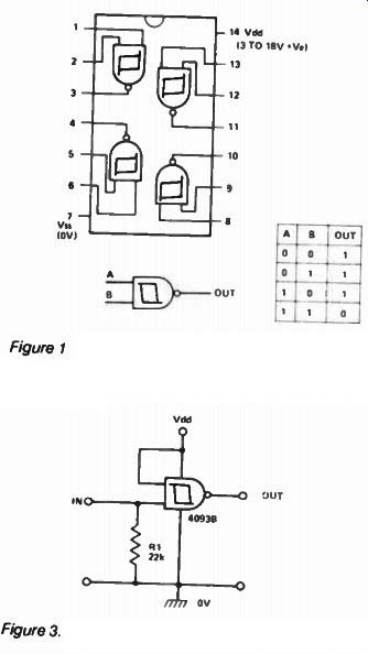
Figure 1 Functional diagram of the 4093 and operating truth table (for a single
Schmitt gate). Odd Figure 3 Simple Schmitt trigger with de input.
Figure 3 the input signal is direct coupled to the gate input. In the Figure 4 sine/square converter circuit the in put signal is ac-coupled and the input pin is biased at half-supply via R1 and R2. In the improved sine/square converter circuit of Figure 5, the input pin bias can be adjusted to mid-way between the upper and lower threshold values, to give maximum sensitivity.
Figure 2. As the gates in a 4093 have a NAND function normally, they should be connected as above to operate as an inverting Schmitt trigger.
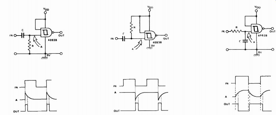
Figure 4 Simple connection for use as a sine/ square converter.
Figure 5. This circuit greatly improves the sensitivity when using the 4093 as a sine/square converter.
---------- Figure 6 To trigger on the rising edge of a pulse, Figure 7. A re- arrangement of Figure 6 to produce Figure 8 How to obtain a delayed and inverted a CR network is added to the input, a falling-edge trigger. version of an input pulse.
Figure 9. How to shorten e pulse by delaying the leading edge. Output is the inverse of the input.
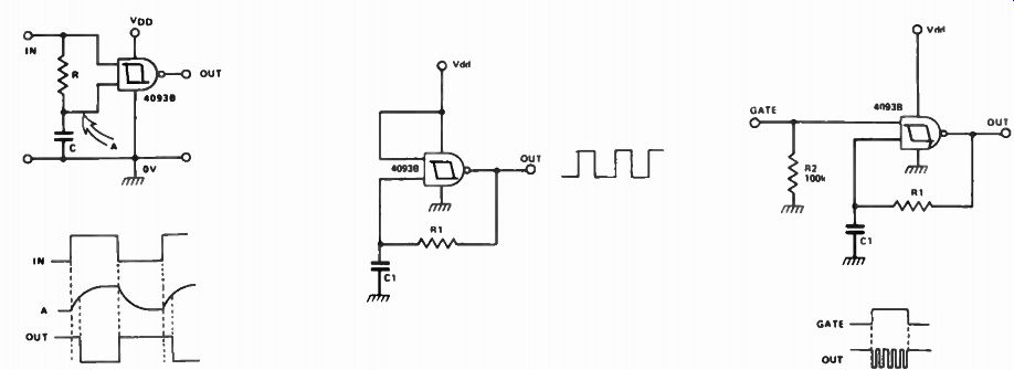
Figure 10 A basic astable multivibrator. The frequency of oscillation depends
on the values of R1 and C1 and the hysteresis.
Figure 11. A variation on the circuit in Figure 10 allowing gated operation of the multivibrator.
Edge Detection
Figures 6 to 9 show a variety of ways of using the 4093 to detect or delay the edges of input pulse waveforms. The figure 6 circuit gives an output pulse on the arrival of the rising or 'leading' edge of an input pulse. The duration of the output pulse is determined by the CR values.
The Figure 7 circuit produces an output pulse on the arrival of the falling or 'trailing' edge of an input pulse. The Figure 8 circuit delays the entire input pulse by a period determined by the CR values. The circuit in Figure 9 delays the leading edge only.
Clock Circuits
Figure 10 shows how a single 4093 gate can be used as an astable multivibrator or 'clock' generator. This circuit gives excellent performance with very clean output edges that are unaffected by supply line ripple and other nasties. The operating frequency is determined by the CR values and can be varied from a few cycles per minute to 1 MHz or so.
The circuit action is such that C1 alternately charges and discharges via R1 . Capacitor C I can be a polarized component.
Figure 11 shows how the basic astable can be gated on and off via an external signal. Note that the circuit is gated ON by a high input, but gives a high output when it is in the OFF state.
The basic astable circuit of Figure 10 produces an inherently symmetrical output waveform. The circuit can be made to produce a non-symmetrical output by providing the timing capacitor with alternate charge and discharge paths, as shown in the circuits of Figure 12. This circuit produces fixed mark space ratio output.
Figure 13 shows a special-purpose voltage-controlled astable which operates only when V,,, rises above the upper Schmitt threshold: the operating
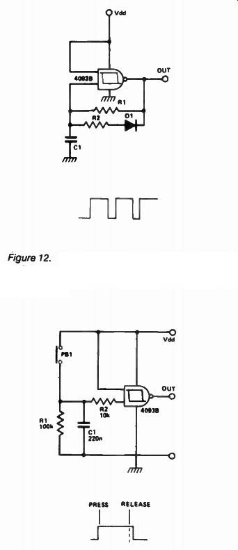
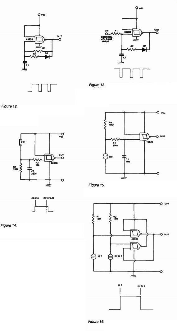
Figure 12 How to obtain a non-symmetrical mark-to- space ratio for the astable multivibrator.
PRESS RELEASE
Figure 14. " Debouncing" a press button switch.
Such circuits are widely used in logic applications.
frequency then rises as V,„ is further increased.
Miscellaneous
Figure 14 is the circuit of a 'noiseless' pushbutton switch, which produces a clean output pulse each time PB1 is operated. C1 charges up rapidly when PB1 is closed but discharges slowly with a period that is long ( relative to normal noise spikes) via RI when PB1 is released.
The output of the circuit in Figure 15 goes high when the input contacts are touched. A latching or 'bistable' touch activated switch is shown in Figure 16.0 Figure 13 The frequency of the astable may be varied by varying Vin shown here. However, Vin must be higher than the upper Schmitt threshold to start with. As you increase Vin, the frequency will increase.
Figure 15 A touch switch that provides a high output when operated. If you swap R1 and SW the output goes low when you touch SW.
Figure 16 A latching' or bistable' touch switch using two gates from the 4093.