Here's a cookbook lef of voltage regulator circuits and techniques covering everything from simple zeners to three-terminal regulators from UK correspondent Ray Marston, with additional material from staff.
ONE OF THE most common and mundane tasks facing the electronics enthusiast is that of designing voltage regulator circuits, je: circuits that produce a stable and well defined dc output voltage over a wide range of load current variations. These circuits may vary from simple zener networks, de signed to provide load currents up to only a few milliamps, to fixed-voltage high current units for powering logic boards, etc, or to variable-voltage high current units designed to act as general purpose pieces of test gear.
fl - Vz = 5 Vm ZD1 Vout 0V
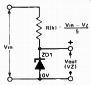
Figure 1. The simplest regulator. The zener regulator is often used to provide
a fixed voltage 'reference' and supplies little or no load current. In such
case a 400 mW zener of appropriate voltage is used and biased at about 5 mA.
The value of R, in kilo-ohms, can be calculated from the formula.
Zener based circuits
A zener diode can be used to produce a fixed reference voltage as shown in Figure 1. Often, the supply voltage (Vin) may be subject to fairly wide variations, causing the zener current to vary over a similarly large range. As long as Vin is always more than a few volts greater than the zener voltage and provided that the zener power rating is not exceeded this variation has only a moderate influence on the output voltage of the zener, which typically has an effective output impedance of a few tens of ohms.
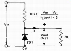
Figure 2. The basic zener regulator can be de signed to supply a load
current of a few milliamps to hundreds of milliamps depending on the zener
power rating. Knowing the required load current, the value of R can be calculated
from the formula.
In most practical voltage regulator applications the zener is simply used to apply a 'reference' voltage to a high gain non-inverting buffer amplifier, which then supplies the required output power. The simplest example of this type of circuit is shown in the series pass regulator circuit of Figure 3.
Op-amp regulators
One way of improving the regulation of the Figure 3 circuit would be to use a Darlington or super-alpha pair of transistors in place of Q1. An even better solution is to use the op-amp plus transistor buffer stage shown in Figure 4.
Choice of circuit would perhaps depend on component availability and the application.
A zener can be used as a very simple voltage regulator, providing load . i . v currents up to a few mA, by determining the value of ' R' as shown in Figure 2.
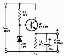
Figure 3. The basic series pass fixed voltage regulator using a zener reference.
This circuit can deliver up to about 100 mA at 11.4 volts. Q1 is basically
an emitter follower, the base being 'clamped' at 12 V by the zener. C1 reduces
the circuit's ac impedance.
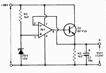
Figure 4. A considerable improvement in regulation is achieved by employing
a high gain op-amp to drive the series pass transistor plus negative feedback
from the dc output. This circuit will deliver up to about 100 mA and the output
voltage stays within a few millivolts of the zener reference for output current
variation from zero to maximum.
The op-amp based regulator of Figure 4 supplies 12V at currents up to 100 mA and gives excellent regulation, despite its simplicity. The op-amp and transistor ( Q1) are interconnected as a unity voltage gain non-inverting de amplifier that has an overall current gain of about one million! The output voltage will be within a few millivolts of the zener reference value and the output impedance is less than one milliohm.
The safe output current driving capacity of the circuit is limited to about 100 mA by the power rating of Q1, which should have a small 'flag' or push on heatsink attached.
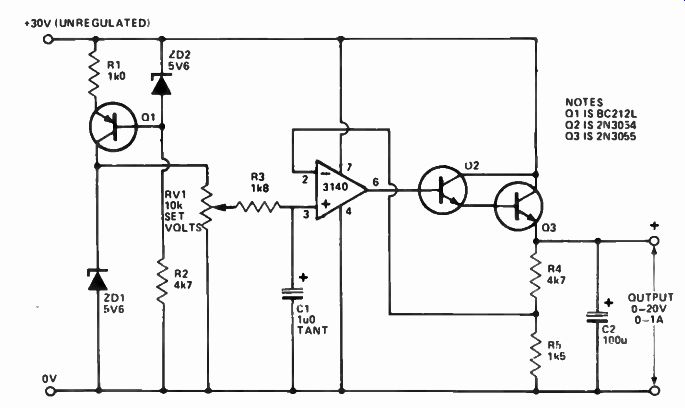
Figure
6. This variation on the Figure 5 circuit permits the output voltage to be
varied between 0 V and 20 V. The 3140 op-amp has a fixed voltage gain of about
four, fixed by R4/R5.
This circuit can be modified to provide greater current output by replacing Q1 with a power Darlington transistor such as the BDV65B. A suitable heatsink should be used.
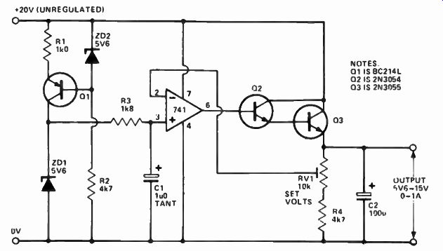
Figure 5. This circuit is a little more sophisticated and performs better
than the Figure 4 circuit. This circuit will deliver up to 1 A output current,
output voltage being variable between 5.6 V and 15 V. Thermal drift is near
zero.
The performance of the basic op-amp circuit of Figure 4 can be improved in a variety of ways, some of which are shown in Figure 5. The first improvement that can be made is to make the zener reference voltage (ZD1) independent of supply voltage variations by powering ZD1 from the output of constant-current generator Ql-R1 ZD2-R2. Next, the zener noise can be eliminated by feeding the reference voltage to the op-amp via low-pass filter R3-C1. Thermal drift effects can be eliminated by making ZD1 a 5V6 type, with near-zero (actually about -0.2 mV/°C) temperature coefficient; the op-amp output voltage can then be set to the desired value ( greater than 5V6) by using feedback components RV1-R4 to set the op-amp's voltage gain at some appropriate value.
Finally, the load current capacity of the circuit can be set to a fairly high value by using a Darlington-connected power transistor in the series pass output stage. Note that Q2 and Q3 could be replaced by a BDV65B Darlington device.
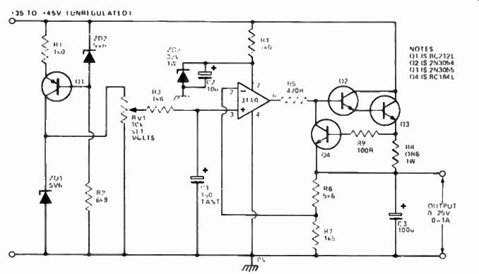
Figure 7 A further refinement is the addition of current limiting and overload
protection. 04 senses the voltage across R8 which is in series with the output.
When the current exceeds 1 A, 04 will be biased on and rob current from the
base of 02 preventing further increase in output current.
The op-amp is protected against excessive supply rail voltage via R4 and ZD3.
Three terminal regulators
Three terminal regulators are remarkably easy to use, as shown in the basic circuits of Figures 8 to 10, which show the connections for making positive, negative and dual regulator circuits respectively; the ICs shown in these examples are 12 V units with current ratings of one amp. Note that a 270 u or greater value disc ceramic capacitor should be connected close to the input terminal of the IC and a 10p. or greater electrolytic to the output.
Figure 8. Circuit for the common-or-garden three-terminal fixed voltage positive
regulator. Note that C2 and C3 should be mounted as close to the regulator's
terminals as is physically possible.
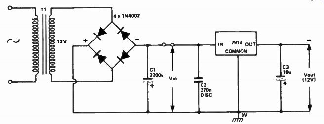
Figure 9. The negative voltage rail counterpart of Figure 8. Don't forget
heatsinks.
These capacitors should be connected as close to the device's terminals as is physically possible. They can be quite good RF oscillators if this is not done correctly! The output voltage of a three terminal regulator is referenced to the `common' terminal of the IC, which is normally grounded. Most regulator ICs draw quiescent currents of a few mA, which flow to ground via the common terminal. The regulator output voltage can thus be 'jacked up' from the designed value by simply biasing the `common' terminal with a suitable voltage.
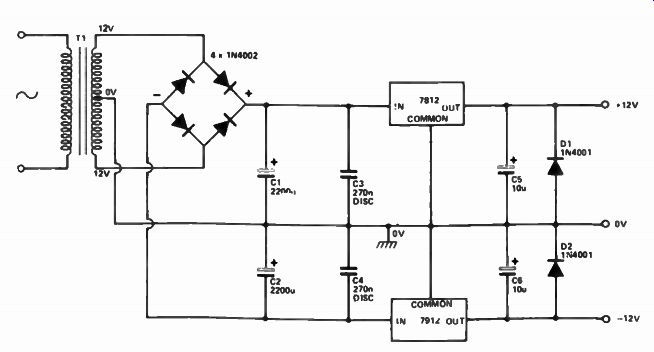
Fig. 10. Circuit of a dual positive/negative power supply employing 1 A three-terminal
regulators.
There are two simple ways to do this.
The first is shown in Figure 11. The required extra voltage is obtained by passing the IC's quiescent current through a trimpot (RV1). The trimpot is then set to provide the required output voltage. Quiescent current is typically 7 mA to 11 mA. This technique is adequate in most applications, although the output voltage obviously shifts slightly with changes in the IC's quiescent current and thus regulation is degraded a little.
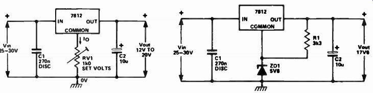
Figure 11. A very simple method of varying the output voltage of a three-
terminal regulator. Regulation is slightly affected
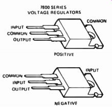
Figure 12 The output voltage can be jacked up' by inserting an appropriate
zener in series with the regulator's common lead.
The output voltage of a three terminal regulator can be increased by a fixed amount by connecting a suitable value zener in series with the common terminal as shown in Figure 12. Output voltage is then the regulator voltage plus the zener voltage, in this case, 17.6 volts. Note that the quiescent current from the common terminal of the IC may not be sufficient to drive the zener and extra bias current is best provided.
Here, R1 serves that purpose.
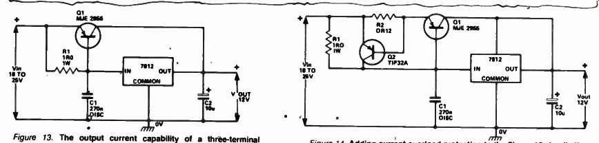
Figure 13 The output current capability of a three- terminal regulator can
be boosted by using an external series pass transistor as illustrated. This
circuit can deliver up to 5A.
Figure 14 Adding current overload protection to the Figure 13 circuit. It a wise idea, even though three-terminal regulators generally incorporate thermal shutdown protection,
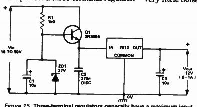
Figure 15. Three-terminal regulators general have a maximum input voltage
rating of 40 V. Where the input may vary widely, at times exceeding the device's
limit, this circuit provides protection by using a 'pre-regulator'.
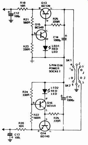
Figure 16. A low noise regulator is necessary in some applications, in which
case zeners cannot be used as they generate noise. LEDs can be used as 'quiet'
voltage reference sources, as illustrated in the +/- 6 V regulators from David
Tilbrook's Series 4000 Moving Coil Preamp project.
More current The output current capacity of à three: terminal regulator can readily be boosted via an external transistor as shown in Figure 13. This circuit, al though it looks familiar, is a little unusual. At low load currents, less than 0.6 volts is developed across R1 and Q1 will not turn on. Thus, all the load current will be supplied by the 7812 regulator. When the load current is greater than about 600 mA, the voltage developed across R1 will be sufficient to turn Q1 on and Q1 will commence delivering current to the load.
This circuit can supply up to 5 A. Note that Q1 will need to be mounted on a substantial heatsink, capable of dissipating 60W. Protection Overcurrent or overvoltage protection for three terminal regulators can be provided relatively easily. Overcurrent protection for the Figure 13 circuit is illustrated in Figure 14. All it needs is a transistor and a resistor. When the current through R2 (a 0.12 ohm resistor) exceeds 5 A, the voltage across it will turn on Q2, robbing base current from Q1, thus current limiting the output. The 7812 will go into its switch-on/ switch-off protection mode.
To protect a three terminal regulator 1 from damage that may, result from excessive supply line voltage, a 'pre regulator' circuit is added. This is illustrated in Figure 15. You will recognize components Q1, R1, C 1 and ZD1 as a simple zener-based series pass regulator (as in Figure 3). Three terminal regulators can with stand no more than 40 V maximum between the input and common terminals, so this circuit limits the voltage applied to about 27V. Note that Q1 should be mounted on a heatsink capable of dissipating 25 W. The LED as a regulator A low noise regulator can be made using a LED as the reference element. David Tilbrook used this technique in the Series 4000 moving-coil preamp (ETI-473, Oct '79). The usual reference element for discrete voltage regulators is a zener. As these devices operate in the reverse biased mode, they are inherently noisy and will put noise on the regulated supply rail. This is likely to degrade the performance of low noise, low level circuits supplied by the regulator.
The circuit of the ±6 V regulated supply for the ETI-473 moving-coil pre amp is reproduced here. A red LED operated in the forward-biased mode drops a constant 1.65 V and generates very little noise. The reference LEDs in the circuit here are LED1 and LED2.
Series regulators Q13 and Q14 regulate the incoming ± 12 V. The potential dividers R21/R23 and R22/R24 divide the voltage present at the output of the regulators and drive transistors Q15 and Q16, and the LEDs. The base emitter junction in series with each LED will drop 0.6 V; to this is added the LED forward drop of 1.65 V. Thus, whenever the voltage present at the junction of the voltage divider resistors tries to increase above 2.3 V, Q15 and Q16 will increasingly conduct, decreasing drive to the bases of Q13 and Q14 respectively.
Noise on the regulated supply rails is further reduced by the C-R networks, C12/R19 and C13/R20.