The humble diode can extricate you from some difficult circuit problems, be it in logic or linear applications.
by Ray Marston
THERE ARE numerous occasions when one needs a basic gate circuit or two and is faced with the possibility of having to wastefully commit an entire IC to this simple function. Alternatively, it may be the case that the inputs to a gate come from such widely separated points of a circuit that the use of an IC in a particular application will result in an excessively complicated pc board layout. In both of these instances, a simple diode gate may offer an ideal solution to the problem.
Figure 1 shows the practical circuit of a three input diode OR gate. The circuit is simple, reasonably fast, very cost effective and can readily be expanded to accept any number of inputs by merely adding one more diode to the circuit for each new input.
The diode OR gate can be converted to a NOR type by either feeding its output through an NPN transistor inverting stage, as shown in Figure 2a, or by feeding its output through any type of IC inverting stage that happens to be 'spare' in the circuit you are playing with, as shown in Figure 2b.
Figure 3 shows the connections for making a three input diode AND gate.
The circuit can again be expanded to accept virtually any number of inputs by simply adding an appropriate number of diodes.
The AND gate can be converted to a NAND type by feeding its output through a pnp transistor or an IC inverting stage, as shown in Figures 4a and 4b respectively.
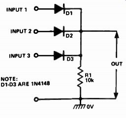
Figure 1. The diode OR gate is simple, but efficient.
It can be expanded to accept any number of inputs by adding extra diodes.
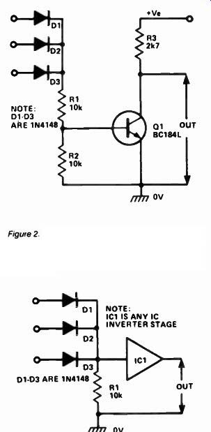
Figure 2 The diode OR gate can be converted to a NOR type by feeding its output
through a transistor, as in ( a) above, or through an IC inverting stage, as
in ( b) below.
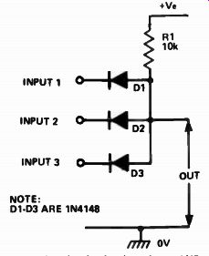
Figure 3 The circuit of a three-input AND gate.
The number of inputs can be increased by adding extra diodes.
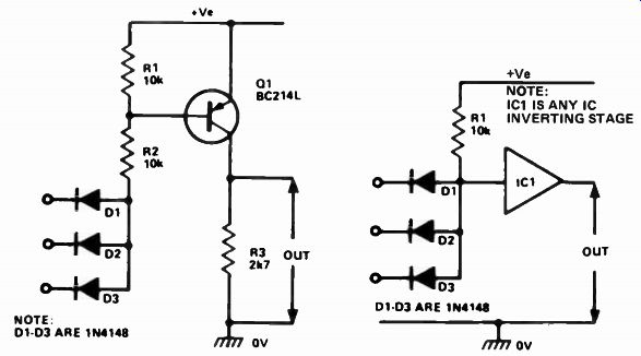
Figure 4 The diode OR gate can be converted to a NAND type by feeding its
output through an inverting stage using either a transistor, as in (a) at left,
or an IC as in (b) at right.
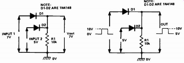
Figure 5 When a diode OR gate is used in the linear mode, Vout equals the
greater of the two inputs.

Figure 6 The effect of feeding a pulse to one input and a dc voltage to the
other input of a two-input diode OR gate.
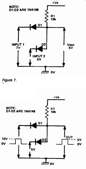
Figure 7. When a diode AND gate is used in the linear mode, Vout equals the
less of the two inputs.
Figure 8. The effect of feeding a pulse to one input and a dc voltage to the other input of a two-input diode AND gate.
Linear operation
Diode AND, and OR gates can be very useful when one or more of their inputs are operated in the linear mode. Figures 5 and 6 show two useful ways of using the two-input diode OR gate in linear applications In the case of the Figure 5 circuit, in which analog voltages are applied to both of the input terminals, the output of the circuit ( ignoring a diode volt drop of about 600 mV) equals the greater of the two input voltages.
Figure 6 shows what happens when a pulse signal is fed to one input of the OR gate and an analog voltage is fed to the other. The output signal comprises a pulse with a peak amplitude equal to that of the input pulse and with a 'zero' value equal to the analog in put voltage.
Figures 7 and 8 show similar circuits based on the two-input diode AND gate.
In the Figure 7 circuit, where analog voltages are fed to both inputs, the output ( ignoring a diode volt drop 'gain' of about 600 mV) equals the lesser of the two inputs.
In the case of the Figure 8 circuit, where a pulse is fed to one input and an analog voltage to the other, the output pulse has a peak amplitude equal to that of the analog input voltage.
Diode volt drops
We've mentioned above that the output of the 'analog' diode gate may be 'within a diode volt drop' of the input signal. The magnitude of this 'volt drop' depends on the type of diode that is in use, on the magnitude of the diode for ward current and on the temperature of the diode junction. All silicon diodes have a negative temperature coefficient of about - 2 mV/°C. Figures 9 and 10 show typical volt drop curves for the popular 1N4148 and 1N4001 silicon diodes at 25°C. The graph of Figure 9 spans the current range 100 uA to 1 mA and the graph of Figure 10 spans the range 1 mA to 50 mA.
Note that the 1N4148 volt drop typically ranges from 519 mV at 100 uA to 874 mV at 50 mA, compared to the 1N4001's range of 441 mV at 100 uA to 744 mV at 50 mA.
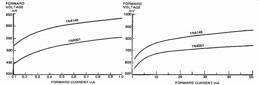
Figure 9. Diode volt-drop curves for the 1N4001 and 1N4148 diodes over the
100 uA to 1 mA current range.
Figure 10. Diode volt-drop curves for the 1N4001 and 1N4148 diodes over the 1 mA to 50 mA current range. Note that these two diode types are the most commonly used (highest volume sales of any single component).
A point of particular note about the 1N4001 curve is that its volt drop of 714 mV at 25 mA increases by only a fraction over 4% (to 744 mV) when the forward current is doubled, to 50 mA. In other words, the diode has a voltage-to current coefficient of about 0.04%/% in this current range. The diode can thus be used as a reasonably stable voltage reference at these current levels but has a negative temperature coefficient of about - 0.3%/°C. Constant current generator Figure 11 shows how the 'voltage reference' characteristics of the 1N4001 can be put to good use in a simple constant current generator circuit that can be used for re-charging Ni-Cad cells or for linearly charging large capacitors, etc.
Here, two 1N4001s are wired in series and operated at a current level of roughly 50 mA. Consequently, the voltage across Rx is equal to the volt drop of the two diodes minus the base-emitter volt of Q1 ( about 700 mV), which gives an Rx voltage of about 700 mV. The emitter (and hence collector) current of Q1 is thus approximately 700/Rx in ( mA). To give an idea of the magnitude of things, an Rx value of 1R2 ( 1.2 ohms) gives an output current of about 600 mA, 3R9 (3.9 ohms) gives about 200 mA, and 6R8 (6.8 ohms) gives about 100 mA. All in all, a simple but very useful circuit.
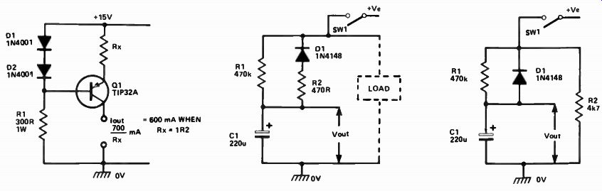
Fig. 11. A simple and very useful current generator.

Figure 12. An example of the use of a diode to rapidly discharge a timing
capacitor when the power supply connection is broken.

Figure 13. A modification to the Figure 12 circuit.
Diode protection circuits
To wrap up these Lab. Notes, let's take a quick look at some diode protection circuits. By 'protection' we mean circuits that are designed to insure devices against irreversible damage and also circuits that are designed to pre vent simple malfunctioning. Figures 12 to 15 show four circuits in this latter category.
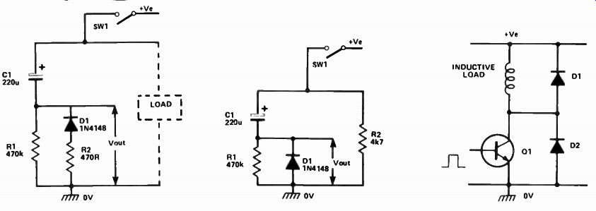
Figure 14 A basic variant of the Figure 12 circuit.

Figure 15 A basic variant of the Figure 13 circuit.

Figure 16. An example of the use of diodes to protect a pulse-driven common
emitter amplifier with an inductive collector load.
In the case of Figure 12, we have a basic time constant circuit in which a rising voltage, with a time constant of about 100 seconds, is developed across C 1 each time SW1 is closed. This voltage may be used to activate some additional circuitry. The problem is that, once C 1 has charged up it has no means of rapidly discharging again (resetting) once SW1 is opened. If there is a load in parallel with the C-R network, as shown dotted in the diagram, C 1 will of course discharge via R1 and the load but then has a very long time constant (greater than 100 seconds). An easy way round this problem is to connect a discharge diode in parallel with R1 as shown in Figures 12 and 13.
If there is a low-impedance load in parallel with the C-R network a current-limiting resistor must be wired in series with the discharge diode, as shown in Figure 12. If there is no load in parallel with the C-R network then an artificial load must be provided to complete the discharge path, as shown in Figure 13.
IN INDUCTIVE LOAD
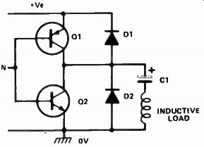
Figure 17 An example of the use of diodes to protect the complementary emitter
follower output stage of a power amplifier that is used to drive an inductive
load.
Figures 14 and 15 show two basic variations of the above circuits in which the C and R networks are configured to give a falling output voltage across R 1 . Finally, Figures 16 and 17 show ways of using diodes to protect two types of transistor circuit from destructive damage. Figure 16 shows how to protect a pulse-driven common-emitter amplifier that has a highly inductive collector load, such as a transformer or a relay coil. Very high back EMFs can be gene rated by inductive loads and can easily destroy transistor junctions. In the dia gram D1 prevents the collector of Q1 from being driven above the positive supply rail value by these back EMFs and D2 prevents it from being driven negative.
Figure 17 shows how a similar type of protection can be given to the complementary emitter follower output stages of a power amplifier used to drive highly inductive loads. This circuit can give good protection to hi-fi amplifiers in which the speakers may be inadvertently plugged in at a moment when the amplifier is being hard driven. The protection diodes must have a current rating that is compatible with the inductive (speaker) load.