DESCRIBED BY R. M. MARSTON
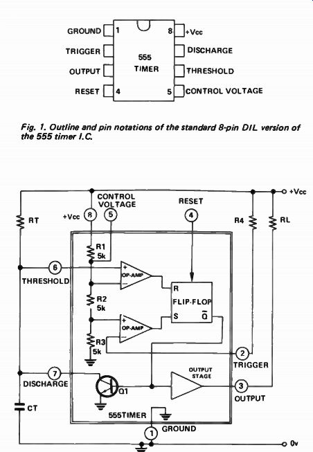
Fig. 1. Outline and pin notations of the standard 8-pin OIL version of the
555 timer I. C.
Fig.
2. Functional block diagram (within the square) of the 555 timer Lc., together
with the connections for using the Lc. as a basic monostable generator or timer.
THE 555 TIMER is a highly versatile low-cost IC specifically designed for precision timing applications. It can also be used in monostable multi-vibrator, astable multivibrator, and Schmitt trigger applications. The device was originally introduced by Signetics, but is now available from many other manufacturers.
The 555 has many attractive features. It can operate from 4.5v to 16v. Its output can source ( supply) or sink ( absorb) any load current up to a maximum of 200 mA, and so can directly drive loads such as relays, LED's, low-power lamps, and high impedance speakers. When used in the 'timing' mode, the IC can readily produce accurate timing periods variable from a few microseconds to several hundred seconds via a single R- C network. Timing periods are virtually independent of supply rail voltage, have a temperature coefficient of only . 005% per degr. C, can be started via a TRIGGER command signal, and can be aborted by a RESET command signal.
When used in the monostable mode, the IC produces output pulses with typical rise and fall times of a mere 100 nS. It can be made to produce pulse-width modulated ( PWM) pulses in this mode by feeding fixed frequency clock pulses to the TRIGGER terminal and, by feeding the modulation signal to the CONTROL VOLTAGE terminal.
When used in the astable mode both the frequency and the duty cycle of the waveform can be accurately controlled with two external resistors and one capacitor. The output signals can be subjected to frequency sweep control, frequency modulation ( FM), or pulse-position modulation ( PPM) by applying suitable modulation signals to the CONTROL VOLTAGE terminal of the IC.
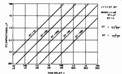
Fig. 3. 555 time delays
for different values of resistance and capacitance.
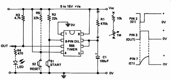
Fig. 4. Circuit and waveforms of simple manually-triggered 50 second timer
or pulse generator.
HOW IT WORKS
The 555 is available under a variety of specific type numbers but is generally referred to simply as a '555 timer.' The device is available in a number of packaging styles, including 8 and 14-pin dual-in-line ( DIL) and 8- pin TO-99 types. Throughout this article all circuits are designed around the standard 8-pin DI L versions of the device.
Figure 1 shows the outline and pin notations of the standard 8-pin DIL version of the 555, and Fig 2 shows the function al block diagram of the same device (within the double lines), together with the connections for using it as a basic mono stable generator. The following explanation of device operation assumes that the 555 is used in the monostable configuration shown in Figure 2.
The 555 houses two diodes, 15 resistors, and 23 transistors.
These components are arranged one voltage-reference potential divider, two voltage, comparator op-amps, one R-S flip flop, a low-power complementary output stage, and a slave transistor. The voltage-reference potential divider comprises three 5 k-ohm, resistors in series, and is connected across the sup ply lines. Consequently, 2/3 Vcc appears at the junction of the upper two resistors of the potential divider, and is fed to one input terminal of the upper voltage-comparator op-amp and 1/3 Vcc appears at the junction of the two lower resistors of the potential divider, and is fed to one input terminal of the lower voltage-comparator op-amp. The outputs of the two comparators control the R- S flip-flop, which in turn controls the states of the complementary output stage and the slave transistor. The state of the flip-flop can also be influenced by signals applied to the pin 4 RESET terminal.
When the monostable or timing circuit of Fig 2 is in its quiescent state, the pin 2 TRIGGER terminal of the chip is held high via R1. Q1 is driven to saturation and forms a short circuit across external timing capacitor CT, and the pin 3 output terminal of the IC is driven to the low state. The mono stable action can be unitiated by applying a negative-going trigger pulse to pin 2. As this pulse falls below the 1/3 Vcc, reference value of the built-in potential divider the output of the lower voltage comparator op-amp changes state and causes the R- S flip-flop to switch over. As the flip-flop switches over it cuts off Q1 and drives the pin 3 output of the chip to the high state.
As Q1 cuts off it removes the short from timing capacitor CT, so CT starts to charge exponentially towards the supply rail voltage until eventually the voltage across CT reaches 2/3 Vcc. At this point the upper voltage comparator op-amp changes state and switches the R- S flip-flop back ot its original condition, so Q1 turns on, rapidly discharging CT, and simultaneously the pin 3 output of the IC reverts to its low state.
The monostable operating sequence is then complete. Note that, once triggered, the circuit cannot respond to additional triggering until the timing sequence is complete, but that the sequence can be aborted at any time by feeding a negative going pulse to pin 4.
The delay time of the circuit, in which the pin 3 output is high, is given as
t = 1.1 R C
where t = mS, AT = Id- 2, and CT = µF.
Figure 3 shows how delays from 10µS to 100 seconds can be obtained by selecting suitable values of CT abd RT in the range 0.001µF to 100 uF and 1 k- ohm to 10 MS- 2 or greater than 20 MS- 2, and capacitor CT must always be a low-leakage component.
Note that the timing period of the circuit is virtually independent of the supply voltage but that the period can be varied by applying a variable resistance or voltage between the ground and pin 5 CONTROL VOLTAGE terminals of the chip.
This facility enables the periods to be externally modulated or compensated.
The pin 3 output terminal of the IC is normally low, but switches high during the active monostable sequence. The output can either source or sink currents up to a maximum of 200 mA, so external loads can be connected between pin 3 and either the positive supply rail or the ground rail, depending on the type of load operation that is required.
The output switching rise and fall times are typically about 100 nano-seconds. Having cleared up these points, let's now go on and look at some practical applications of the 555 timer I.C.
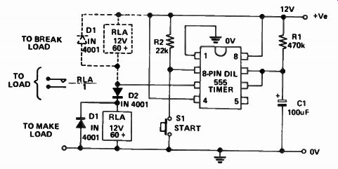
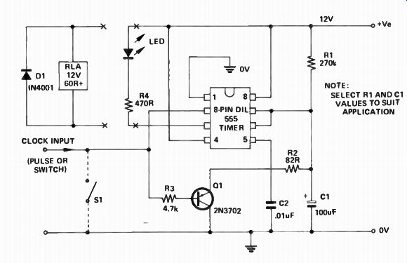
Fig. 5. Relay-output timer makes or breaks connection to load for pre set
period of 50 seconds when S, is momentarily operated.
50 SECOND TIMER
This 50 second timer or pulse generator gives a direct voltage output at pin 3 which is normally low, but goes high for the duration of the timing period. Optional components R4 and LED ( shown dotted) give a visual indication of the timer action. The circuit works in the same basic way as already described, except that the timing action is initiated by momentarily shorting pin 2 to ground via START switch Si Note from the circuit waveforms that a fixed- period output pulse is available at pin 3 and an exponential sawtooth with an identical period is available at pin 7: The sawtooth waveform has a high output impedance.
The basic timer circuit of Fig 4 can be varied in a number of ways. The timing period can be made variable between approximately 1.1 seconds and 110 seconds by replacing R1 with a 10 k-ohm fixed resistor and a 1 M-ohm variable resistor in series.
The period can be further varied, if required, by switch selecting decade values of timing capacitance. The dotted section shows how the circuit can be provided with a RESET facility, so that a timing period can be aborted at any time, by taking pin 4 to the positive supply rail via resistor R5 and wiring RESET switch ohm between pin 4 and ground.
The timing circuit of Fig 4 can be used to drive non inductive loads at currents up to 200 mA directly. They can be used to drive inductive relay loads by using the basic connections shown in Fig 5.
The (Fig 5) circuit is designed to apply a connection to a normally-off external load for a pre-set period of 50 seconds when START switch Si is momentarily closed. The relay is normally off, but turns on for the 50 second period when the timing cycle is initiated. D2 is wired in series with the relay coil to counteract the slight residual voltage that appears at pin 3 of the IC under the OFF condition and thus ensure that the relay turns fully off. The dotted section shows how this circuit can be used to switch off a normally-on load.
Note in Fig. 5 and all other relay-output circuits described here, that the relays used can be any 12 volt types that draw ON currents of less than 200 mA, e.g., that have coil resistances greater than 60 ohm.
The basic relay-driving timer circuit of Fig 5 can be adapted for use in a variety of useful applications. Some typical examples are shown in Figs 6 to 9.
Figure 6 shows the practical circuit of a relay-output general-purpose timer that covers 0.9 seconds to 100 seconds in two decade ranges. The circuit has a RESET facility provided via ohm , so that timing periods can be aborted part way through a cycle if necessary. A noteworthy feature of this circuit is that the maximum timing periods of each decade range of the timer can be precisely pre-set via R5 or R6 , which effectively shunt the built-in potential divider of the 555 and thus influence the timing periods: This facility enables the circuit to give precise timing periods even when wide tolerance timing capacitors are used.
To set up the Fig 6 circuit, first set R1 to maximum value, set RANGE switch S3 to position 1, activate START switch Si, and adjust R5 to give a timing period of precisely 10 seconds. Next, set S3 to position 2, activate START switch Si, and adjust R6 to give a timing period of precisely 100 seconds. All adjustments are then complete, and the timer is ready for use.
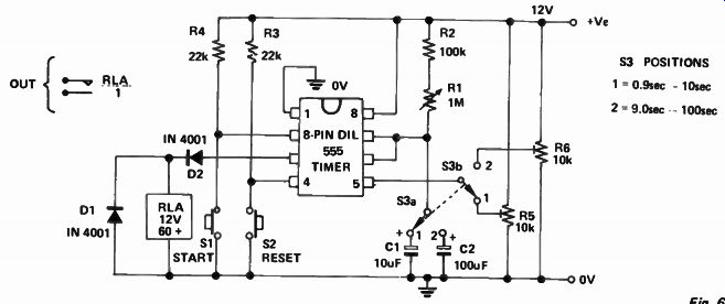
Fig. 6. Relay-output general-purpose timer covers 0.9 sec to 100 sec in two
decade.
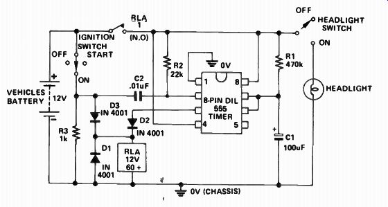
Fig. 7. Automatic delayed-turn-out headlight control system for automobiles.
DELAYED HEADLIGHT TURN-OFF
Figure 7 shows the practical circuit of an automatic delayed turn-off headlight control system for auto-mobiles. This facility enables the owner to use the car lights to illuminate his path for a pre-set time after parking as he leaves the garage or walks along a driveway, etc. The circuit does not interfere with normal headlight operation under actual driving conditions. It works as follows.
When the ignition switch is turned to the ON position current is fed to the coil of the relay via D3 and the 12 volt supply rail, so the relay turns on and contacts R LA/1 close.
As the contacts close they connect the 12 volt supply rail, so the relay turns on and the headlight switch. Thus, under this 'ignition on' condition the headlights operate in the normal way. Note that, since one side of C2 is connected directly to the positive supply rail and the other side is taken to the positive rail via R2, the capacitor is fully discharged under this condition.
'The moment that the ignition switch is turned to the OFF position the D3-derived current supply to the relay coil is broken, and simultaneously a negative-going trigger pulse is fed to pin 2 of the 555 as the C2- R3 junction drops to ground volts and C2 charges up. Relays are inherently slow acting devices, so contacts R LA/1 do not open instantaneously as the ignition switch is turned off. Conversely, the 555 is a very fast triggering device, and the instant that the trigger pulse is generated, via the turn-off action of the ignition switch a timing cycle is initiated and current is fed to the relay coil via output pin 3 of the IC as it goes high. Thus the relay remains on for a pre-set period after the ignition connected to the headlight switch for the duration of this period. With the component values shown this period is roughly 50 seconds.
At the end of the 50 second timing period, pin, 3 of the 555 switches to the low state and the relay turns off. As it does so, contacts R LA/1 open and remove the supply from the timer and the headlight switch, and the headlights turn off. The operating sequence is then complete.
Readers may care to note that the above system of operation is consistent with the practice adopted in many modern vehicles of feeding the headlight switch via the ignition switch, so that the headlights operate only when the ignition is turned on. On older types of vehicle, where headlight operation is independent of the ignition switch, a manually-triggered delayed-turn-off headlight or spotlight control facility can be obtained by using the circuit shown in Fig 8. The action of this circuit is such that, if the vehicle is parked with its lights off, they turn on for a pre-set 50 second momentarily closed, and at the end of this period turn off again automatically.
The (Fig 8) circuit uses a relay with two sets of normally open relay contacts. The timing sequence is initiated by momentarily closing push-button switch Si. Normally, both Si and the relay contacts are open, so zero power is fed to the timer circuit and the lights are off. C2 discharged under this condition.
When S1 is momentarily closed power is fed directly to the relay coil, and the relay turns on. As the relay turns on, contacts R LA/2 close and apply power to the vehicle lights and contacts R LA/1 close and apply power to the timer circuit, but pin 2 of the IC is briefly tied to ground via C2 and R3 at this moment, so a negative trigger pulse is immediately fed to pin 2 and a timing cycle is initiated. Consequently, pin 3 of the 555 switches high at the moment that the relay contacts close, and thus locks the relay into the ON condition irrespective of the subsequent state of START switch Si so the lights remain on for the duration of the 50 second timing cycle. At the end of the timing cycle pin 3 of the IC switches to the low state, so the relay turns off and contacts RLA/1 and RLA/2 open, disconnecting power from the timing circuit and the lights. The operating sequence is then complete.
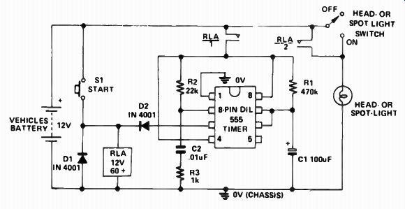
Fig. 8. Manually-triggered delayed-turn-off head- or spot-light control system
for auto mobiles.
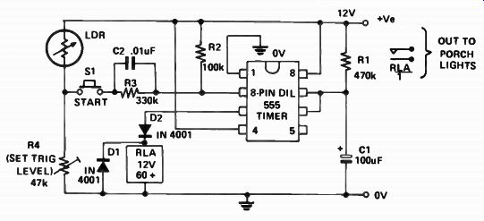
Fig. 9. Automatic porch light turns on for a pre-set period only when triggered
at night.
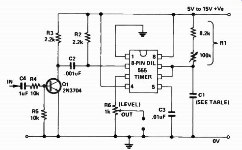
Fig. 10a: Simple add-on pulse generator is triggered by rectangular input
signals: circuit can be used at trigger frequencies up to 100 kHz.
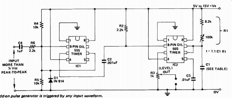
Fig. 10b: Improved add-on pulse generator is triggered by any input waveform.
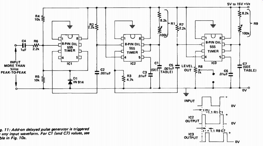
Fig. 11: Add-on delayed pulse generator is triggered by any input waveform.
For C1 (and C1) values, see table in Fig. 10a.
PORCH LIGHT
Finally, to conclude this 'Timer Circuits' section of the 555 story, Fig 9 shows the circuit of a relay-output automatic porch light control unit that turns the porch lights on for a pre-set 50 second period only when suitably triggered at night-time or under 'dark' conditions: The circuit is triggered via switch Si, which may take the form of a microswitch activated by a porch gate or a pressure-pad switch activated by body weight and concealed under a porch mat or rug.
The operation of the Fig 9 circuit relies on the fact that for correct timer operation the negative-going trigger pulse that is fed to pin 2 of the IC must fall below the internally controlled ' 1/3 Vcc' voltage value of the 555. If the trigger pulse does not fall below this value, timing cycles can not be initiated by the trigger signal.
In this design, light-dependent resistor LDR and preset resistor R4 are wired in series as a light-dependent potential divider. One side of switch S1 is taken to the output of this potential divider, and the other side of the switch is taken to pin 2 of the IC via the C2- R3 combination. Under bright or daylight conditions the LDR acts as a low resistance, so a high voltage appears at the output of the potential divider.
Consequently, the act of closing Si causes a voltage pulse much higher than ' 1/3 Vcc' to be fed to pin 2 of the chip, so the timer is not triggered via S1 under the 'daylight' condition.
Conversely, the LDR acts as a high resistance under dark or 'night' conditions, so a low voltage appears at the output of the potential divider. Consequently, the act of closing Si causes a voltage pulse much lower than ' 1/3 Vcc' to be fed to pin 2 of the IC, so the time circuit is triggered via S1 under the 'night' condition.
In practice, the LDR can be any cadmium-sulphide photo cell that presents a resistance in the range 1 k- ohm to 100 k- ohm under the required minimum 'dark' turn-on condition, and R4 can be adjusted to preset the minimum 'dark' level at which the circuit will trigger. Note that the trigger signal is fed to pin 2 of the IC via the C2- R3 combination, which act as a trigger signal conditioning network that effectively isolates the d.c. component of the LDR-R4 potential divider from the trigger pin of the IC.
MONOSTABLE PULSE GENERATOR CIRCUITS
All the 555 timer circuits that we have looked at so far act essentially as monostable multivibrators or pulse generators. The 555 can be used as a conventional electronically triggered monostable multivibrator or pulse generator by feeding suitable trigger signals to pin 2 and taking the pulse output signals from pin 3. The IC can be used to generate good output pulses with periods from 5 ¡ is to several hundred seconds. The maximum usable pulse repetition frequency is approximately 100 kHz.
The trigger signal reaching pin 2 must be a carefully shaped negative-going pulse. Its amplitude must switch from an OFF value greater than 2/3Vcc to an ON value less than 1/3 Vcc (triggering actually occurs as pin 2 drops through the 1/3 Vcc value). The pulse must have a width greater than 100 ns but less than that of the desired output pulse, so that the trigger pulse is removed by the time the monostable period terminates.
One way of determining a suitable trigger signal for the 555 monostable circuit is to convert the input signal to a good square wave that switches between ground volts and the full positive supply rail voltage, and then couple this square wave to pin 2 of the IC via a simple short time-constant C- R differentiating network, which converts the leading or trailing edges of the square wave into suitable trigger pulses. Figure 10a shows a practical circuit that uses this basic principle, but is intended for use only with input signals that are already of square or pulse from.
Here, transistor 01 converts the rectangular input signal into a signal that switches between the ground and positive voltage rails, and the resulting signal is fed to pin 2 via the differentiating network. The circuit can be used as an add on pulse generator in conjunction with an existing square or pulse generator. Variable-amplitude output pulses are available from pin 3 via variable potential divider R6. The output pulse widths can be varied over more than a decade range via R1, and can be switched in overlapping decade ranges by using the values of C1 listed in the table. With the component values shown the pulse width is fully variable from 94s to 1.2 seconds. Note that C3 is used to decouple the pin 5 CONTROL VOLTAGE terminal and improve the circuit stability.
Figure 10b shows how the above circuit can be modified so that it can be driven from any type of input waveform, including sine waves. Here, IC1 is connected as a simple Schmitt trigger, which converts all input signals into rectangular output signals, and these rectangular signals are used to drive the IC2 monostable circuit in the same way as described above The Fig 10b circuit can thus be used as an add-on pulse generator in conjunction with an existing waveform generator of any type that produces output signals with peak to-peak amplitudes greater than 1/2 Vcc.
Figure 11 shows two basic monostable pulse generators connected in series to make a delayed pulse generator. IC1 is used as a Schmitt trigger and IC2 controls the delay width and IC3 determines the output pulse width: The final output pulse appears some delayed time after the initial application of the trigger signal. This circuit can be made into a self-contained instrument by building it into the same cabinet as a simple square wave generator which can be used to provide the necessary drive signals.
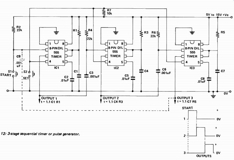
Fig. 12: 3-stage sequential timer or pulse generator.
Any number of basic monostable pulse generators can be wired in series to give a sequential form of operation. Figure 12 for example, shows the circuit and wave-forms of a 3 stage sequential generator, which can be used to operate lamps or relays, etc., in a pre-programmed time sequence once an initial START command is given via push-button switch S1.
Note that the pin 4 RESET terminal of all ICs are shorted together and positively biased via R7, and that these terminals can be shorted to ground via SET switch ohm: This SET switch should be closed at the moment that power is first applied to the circuit, to ensure that none of the ICs falsely triggered at this moment.
Finally, three or more monostable circuits can be connected, via C9, in a continuous loop, with the output of the last monostable feeding back to the input of the first mono stable, to form a 'chaser' circuit in which the sequential action repeats to infinity. This type of circuit can be used to drive lamp or LED displays, etc. Note that the circuit is again provided with the ohm SET facility, so that the circuit can be emptied at the moment that power is first applied.
ASTABLE MULTIVIBRATOR CIRCUITS
Figure 13 shows a basic 1kHz astable multivibrator, together with the formulas that define the timing of the circuit. Note that TRIGGER pin 2 of the chip is shorted to the pin 6 THRESHOLD terminal, and that timing resistor R2 is wired between pin 6 and DISCHARGE pin 7.
When power is first applied to the circuit C1 starts to charge exponentially ( in the normal monostable fashion) via the series R1- R2 combination, until eventually the C1 voltage rises to 2/3 Vcc. At this point the basic monostable action terminates and DISCHARGE pin 7 switches to the low state. C1 then starts to discharge exponentially into pin 7 via R2, until eventually the C1 voltage falls to 1/3 Vcc, and TRIGGER pin 2 is activated. At this point a new monostable timing sequence is initiated, and C1 starts to recharge towards 2/3 Vcc via R1 and R2. The whole sequence then repeats add infinitum, with C1 alternately charging towards 2/3 Vcc via R1- R2 and discharging towards 1/3 Vcc via R2 only.
Note in the above circuit that, if R2 is very large relative to R1, the operating frequency of the circuit is determined essentially by the R2 and C1 values, and that a virtually sym metrical output waveform is generated. The graph of Fig 14 shows the approximate relationship between frequency and the C1- R2 values under the above condition. In practice, the R1- R2 values of the circuit can be varied from 1 Idt up to tens of megohms. Note, however, that R1 has a significant effect on the total current consumption of the circuit, since pin 7 of the IC is virtually grounded during half of the timing sequence. Also note that the duty cycle or mark/space ratio of the circuit can be pre-set at a non-symmetrical value, if required, by suitable choice of the R1 and R2 values.
The basic circuit of Fig 13 can be usefully modified in a number of ways. Fig 15, for example, shows how it can be made into a variable-frequency square wave generator by replacing R2 with a fixed and variable resistor in series. With the component values shown the frequency can be varied over the approximate range 650 Hz-7.2 kHz via R2.
Figure 16 shows how the circuit can be further modified so that its MARK and SPACE periods are independently variable over the approximate range 7.5ps to 750ps. Here, timing capacitor C1 alternately charges via R1- R2- D1 and discharges via R3- R4- D2.
Figure 17 shows how the circuit can be additionally modified so that it acts as fixed-frequency square wave generator with a mark/space ratio or duty cycle that is fully variable from 1% to 99%. Here, C1 alternately charges via R1 and the top half of R2 and via D1, and discharges via D2- R3 and the lower half of R2. Note that the sum of the two timing periods
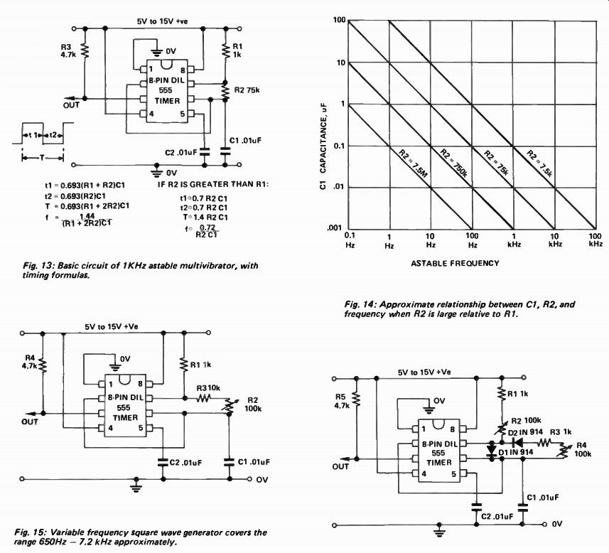
Fig. 13: Basic circuit of 1KHz astable multivibrator, with timing formulas.
Fig. 15: Variable frequency square wave generator covers the range 650Hz - 7.2 kHz approximately.
Fig. 14: Approximate relationship between C1, R2, and frequency when R2 is large relative to R1.
Fig. 16: Astable multi with mark and space periods independently variable over the approximate range 7.5/is to 750ps.
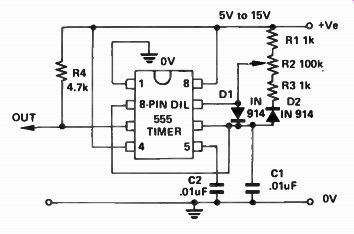
Fig. 17: Astable multi with duty cycle variable from 1 to 99% with frequency
approximately constant at 1.2 kHz.
is virtually constant, so the operating frequency is almost independent of the setting of R2.
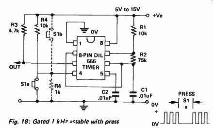
Fig. 18: Gated 1 kH7stable with press
GATING A 555 ASTABLE
The 555 astable circuit can be gated ON or OFF, via either a switch or an electronic signal, in a variety of ways. Figs 18 and 19 show two basic ways of gating the IC via a switch.
In Fig 18 the circuit is gated via the pin 4 RESET terminal.
The characteristic of this terminal is such that, if the terminal is biased significantly above a nominal value of 0.7 volts, the astable is enabled, but if the terminal is biased below 0.7 volts by a current greater than 0.1 mA (by taking the terminal to ground via a resistance less than 7 k-o, for example) the astable is disabled and its output is grounded. Thus, the Fig 18 circuit is normally on but can be turned off by closing Si and shorting pin 4 to ground, while the circuit shown in dotted lines is normally gated off via R4 but can be turned on by closing ohm and shorting pin 4 to the positive supply rail.
These circuits can alternatively be gated by applying suitable electronic signals directly to pin 4.
The Fig 19a and 19b circuits are gated via the pin 2 TRIG GER and pin 6 THRESHOLD terminals. The characteristic here is such that the circuit functions as a normal astable only as long as pin 6 is free to swing up to 2/3 Vcc and pin 2 is not biased below 1/3 Vcc. If these pins are simultaneously driven below 1/3 Vcc the astable action is immediately terminated and the output is driven to the high state. Thus, the Fig 19a circuit is normally on but turns off when S1 is closed.
Note that an electronic signal can be used to gate the circuit by connecting a diode as indicated and eliminating S1. In this case the circuit will gate off when the input signal voltage is reduced below 1/3 Vcc.
The Fig 19b circuit is connected so that it is normally gated off by saturated transistor Q1, but can be gated on by closing S1 and thus turning the transistor off. This circuit can be gated electronically by eliminating R5 and S1 and applying a gating signal to the base of Q1 via a 10 ohm limiting resistor. In this case the astable turns off when the input signal is high, and turns on when the input signal is reduced below 0.7 volts or so.
All the 555 astable circuits that we have looked at can be subjected to frequency modulation ( FM) or pulse-position modulation ( PPM) by simply feeding a suitable modulation signal to pin 5. This modulation signal can take the form of an ac signal that is fed to pin 5 via a blocking capacitor, as in the case of Fig 20a or a dc signal that is fed directly to pin 5, as in the case of Fig 20b. The action of the chip is such that the voltage on pin 5 influences the width of the 'mark' pulses in each timing cycle, but has no influence on the 'space' pulses. Thus, since the signal on pin 5 influences the position of each 'mark' pulse in each timing cycle, this terminal provides pulse-position modulation ( PPM), and, since the signal influences the total period of each cycle ( and thus the frequency of the output signal), the terminal also provides frequency modulation ( FM). These facilities are useful in special waveform generator applications, as is shown in the next section.
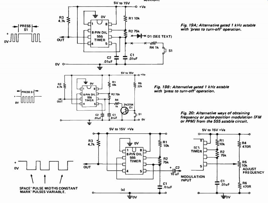
Fig. 19A; Alternative gated 1 kHz astable with ' press to turn-off' operation.
Fig. 19B: Alternative gated 1 kHz astable with 'press to turn-off' operation.
Fig. 20: Alternative ways of obtaining frequency or pulse-position modulation (FM or PPM) from the 555 astable circuit.
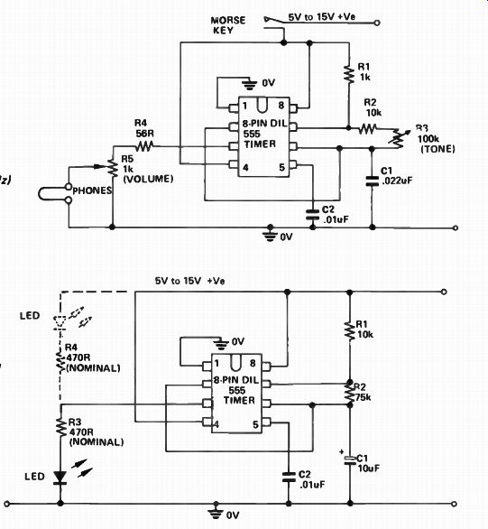
Fig. 21. Code-practice oscillator with variable tone (300 - 3kHz) and variable
volume.
Fig. 22. Single and dual output LED flashers give symmetrical 1 Hz outputs.
MISCELLANEOUS ASTABLE APPLICATIONS
The 555 astable multivibrator has three outstanding ad vantages over other types of astable circuit. First, its frequency can be varied over a wide range via a single resistive control. Second, its output has a low impedance and can source or sink current up to 200 mA. Finally, its operating frequency can readily be modulated by applying a suitable signal to pin 5 of the IC. These features make the device exceptionally versatile, and it can be used in a vast range of practical applications of interest to both the amateur and professional user.
Morse Practice Oscillator
Figure 21 shows how the 555 timer IC can be used as a morse- code practice oscillator. The circuit acts as a normal astable, with frequency variable over the approximate range 300 Hz - 3 kHz via TONE control R3. The 'phone volume is variable via R5, and the 'phones can have any impedance from a few ohms up to megohms. The circuit draws zero quiescent current, since the normally-open morse key is used to connect the circuit to the positive supply rail, which can have any value in the range 5 volts to 15 volts.
Figure 22 shows how the 555 astable circuit can be used in LED flasher applications. This circuit operates at approximately 1 Hz, and has a single LED. The Fig 22 circuit has a single LED output, the dotted section shows how a second may be added, such that one LED is on while the other is off, and vice versa. Any types of LED's can be used in this circuit. Series resistors R1 or H4 determine the ON current of each LED.
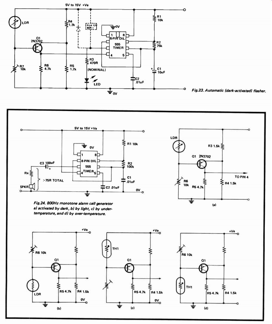
Fig. 23. Automatic (dark-activated) flasher. Fig.24. 800Hz monotone alarm call
generator
a) activated by dark, b) by light, c) by under temperature, and d) by over- temperature.
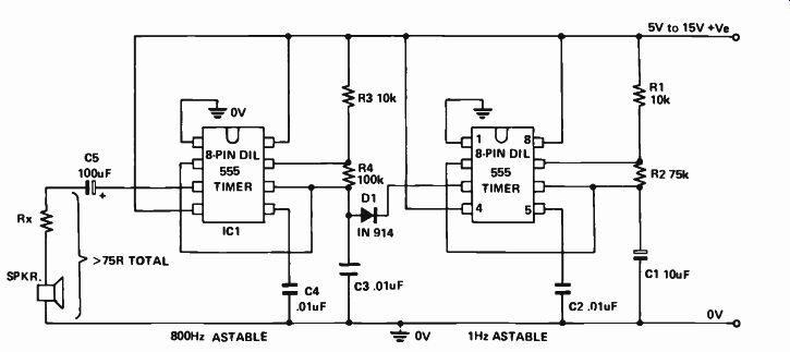
Fig. 25. Pulsed- tone (800H4 alarm call generator.
Figure 23 shows how the Fig 22 circuit can be modified to give automatic dark-activated operation. Here, R4 and R5 are wired as a fixed potential divider that sets 1/2 Vcc on the emitter of Q1. LDR and R7 are wired as a light-sensitive potential divider that applies a variable voltage to the base of Q1, and the collector of Q1 is taken to RESET pin 4 of the IC, which is normally biased to ground via R6.
In use R7 is adjusted so that the voltage to the base of Q1 is greater than 1/2 Vcc under 'daylight' conditions, so Q1 is cut off, but under 'dark' conditions Q1 base is biased below 1/2 Vcc, so it is driven on, thus, under daylight conditions Q1 is cut off, so the 555 astable is disabled, with its output driven low, by 4.7 k-ohm resistor R6 which is wired between pin 4 and ground. Under 'dark' conditions, on the other hand, Q1 is biased on, so pin 4 is positively biased, and the astable operates normally and activates the LED. The LDR used in the above circuit can be any cadmium sulphide photocell that presents a resistance in the approximate range 470 ohm to 10 k ohm under the minimum 'dark' turn on condition.
The dotted section shows how the 555 astable circuit can be used as a 12 volt relay pulser, which turns the relay on and off at a rate of one cycle per second. The relay can be any type with a coil resistance greater than 60 ohm.
Alarm Generator
Figure 24 shows the connections for making an 800 Hz monotone alarm-call generator. The circuit can be used with any supply in the range 5 to 15 volts, and with any speaker impedance. Note, however, that Rx must be wired in series with speakers of less than 75 ohm impedance, and must be chosen to give a total series impedance of at least 75 S1, to keep the peak speaker currents within the 200 mA driving constraints of the 555. The available alarm output power of the circuit depends on the speaker impedance and supply voltage used, but may be as great as 750 uS when a 75 speaker is used with a 15 volt supply.
The above circuit can be modified so that it is activated by darkness ( a), by brightness ( b), by an under-temperature (c), or by an over-temperature ( d). Pin 4 is disconnected from the + Ve supply, and connected to the triggering circuit, which is designed around Q1. This works in the same way as already described for the automatic (dark-activated) LED flasher. The LDR used in the light-activated versions of this circuit can be any cadmium-sulphide photocells that present resistances in the approximate range 470 ohm to 10 k ohm at the desired turn-on levels. The thermistors used in the temperature-activated versions of the circuit can be any negative-temperature-coefficient types that present resistances in the same range at the required turn-on temperatures.
Alarms and Sirens
The next four diagrams show a variety of useful alarm-call generator circuits. The Fig 25 circuit generates an 800 Hz pulsed tone alarm call. Here, IC1 is wired as an 800 Hz alarm generator, and IC2 is wired as a 1 Hz astable which gates IC1 on and off via D1 once every second, thus causing a pulsed-tone output signal to be generated.
The Fig 26 circuit generates a warble-tone alarm signal that simulates the sound of a police siren. Here, IC1 is again wired as an alarm generator and IC2 is wired as 1 Hz astable multi vibrator, but in this case the output of IC2 is used to frequency modulate IC1 via R5. The action is such that the output frequency of IC1 alternates symmetrically between 500 Hz and 440 Hz, taking one second to complete each alternating cycle.
The circuit of Fig 27 generates a 'wailing' alarm that simulates the sound of an American police siren. Here, IC2 is wired as a low frequency astable that has a cycling period of about six seconds. The slowly varying ramp waveform on C1 of this chip is fed to pnp emitter follower Q1, and is then used to frequency modulate alarm generator IC1 via R6. IC1 has a natural centre frequency of about 800 Hz. The circuit action is such that the alarm output signal starts at a low frequency, rises for 3 seconds to a high frequency, then falls during 3 seconds to the low frequency, and so on ad intfinitum.
Finally, to complete this quartet of alarm generator circuits, the Fig 28 circuit generates a siren alarm signal that is a simulation of the ' Red Alert' alarm used in the STAR TREK T.V. program: This signal starts at a low frequency, rises for about 1.15 seconds to a high frequency, ceases for about 0.35 seconds, then starts rising again from a low frequency, and so on add infinitum. The circuit action is as follows: IC2 is wired as a non-symmetrical astable multivibrator, in which C1 alternately charges via R1 and D1, and discharges via R2, thus giving a rapidly rising and slowly falling ' sawtooth' waveform across Cl. This waveform is fed to pnp emitter follower Q1, and is thence used to frequency modulate pin 5 of IC1 via R6. Now, the frequency modulation action of pin 5 of the IC1 astable circuit is such that a rising voltage on pin 5 causes the astable frequency to fall, and vice versa; consequently the sawtooth modulation signal on pin 5 causes the astable frequency to rise slowly during the falling part of the sawtooth and collapse rapidly during the rising part of the sawtooth. The rectangular pin 3 output of IC2 is used to gate IC1 off via npn common emitter amplifier Q2 during the collapsing part of the signal, so only the rising parts of the alarm signal are in fact heard, as in the case of the genuine STAR TREK 'Red Alert'.
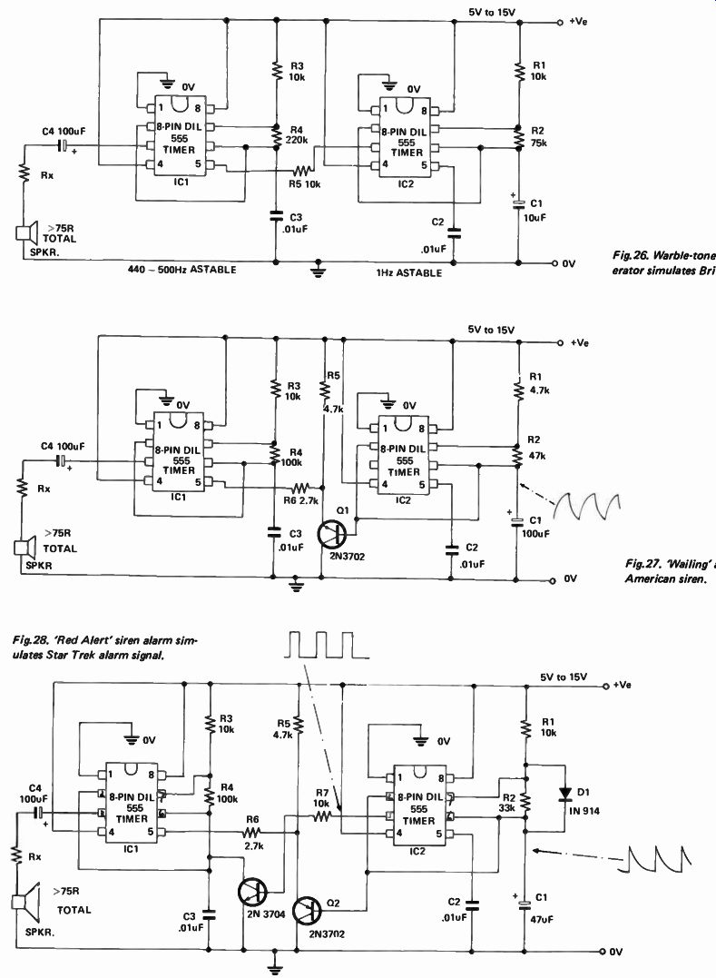
Fig.26. Warble- tone alarm call generator simulates British police siren.

Fig.27. Wailing' alarm simulates American siren.
Fig. 28. 'Red Alert' siren alarm simulates Star Trek alarm signal.
-------------
Miscellaneous Applications
To complete the story of the 555, this final section shows a miscellany of 555 applications, of varying degrees of usefulness. Figure 29 shows how a single 555 can be used as the basis of an event-failure alarm or a missing-pulse detector, which closes a relay or illuminates an LED if a normally recurrent event fails to take place.
The operating theory of the circuit is fairly simple. The 555 is wired as a normal monostable pulse generator, except that transistor Q1 is wired across timing capacitor C1 and has its base taken to TRIGGER pin 2 of the IC via R3: The TRIGGER pin is fed with a train of pulse or switch-derived clock input signals from the monitored event, and the values of R1 and C1 are selected so that the monostable period of the IC is slightly longer than the repetition period of the clock signal.
Thus, each time a clock pulse arrives, a monostable timing period is initiated via pin 2 of the IC, and C1 is discharged and the pin 3 output is driven high via transistor Ql. Before each monostable period can terminate, a new clock pulse arrives, and a new monostable period is initiated, so the pin 3 output terminal remains high so long as clock input pulses continue to arrive within the prescribed period limits. Should a clock pulse be missed, or the clock period exceed the pre-determined limits, however, the monostable period will be able to terminate normally, and pin 3 of the IC will go low and drive the relay or LED on. The circuit thus functions effectively as an event-failure alarm or missing- pulse detector. With the component values shown, the monostable has a natural period of about 30 seconds. This period can be varied via R1 and C4 to satisfy specific requirements.
Fig, 29. Event-failure alarm or missing-pulse detector has relay or LED output.
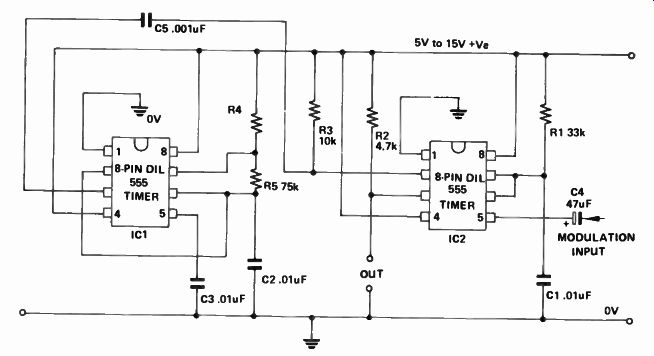
Fig. 30. Pulse-width modulation PWM circuit.
Figure 30 shows how a couple of 555s can be used to make a pulse-width modulation ( PWM) circuit. This circuit can be used for transmitting coded messages, or for applying variable power to a load at maximum efficiency.
Here, IC1 is wired as 1 kHz astable multivibrator, which is used to feed a continuous train of clock pulses to the pin 2 TRIGGER terminal of IC2, which is wired as a normal mono-stable multivibrator or pulse generator and has a natural monostable period of approximately 0.36 mS. The external modulation signal is fed to the pin 5 CONTROL VOLTAGE terminal of the monostable via C4, and determines the instantaneous widths of the generated pulses. Thus, the circuit generates a train of pulse-width modulated ( PWM) pulses at a fixed repetition frequency of 1 kHz.
Scope timebase
Figure 31 shows how a basic 555 monostable multivibrator can be modified so that it generates a linear ramp waveform of fixed duration each time it is triggered: The circuit can form the basis of an excellent oscilloscope time-base generator. The circuit works just like a normal monostable circuit, except that timing capacitor C1 is charged via constant-current generator Q1 during each timing cycle, thus causing a linear ramp voltage to be generated across C1. When a capacitor is charged via a constant-current generator, the voltage across the capacitor rises linearly at a predict able rate that is determined by the magnitudes of the charging current and the capacitance. The relationship can be expressed as: Volts- per-second = I/C, when I is expressed in amps and C is expressed in farads.
In this circuit the charging current can be varied over the approximate range 90 µA to 1 mA via R4, thus giving rates of rise on the 0.01 µF capacitor of 9 V- per- ms to 100 V-per-ms.
Now, remembering that each monostable period of the 555 circuit terminates at the point when C1 voltage reaches 2/3 Vcc, and assuming that a 9 V supply is used ( giving a 2/3 Vcc value of 6 V), it can be seen that the monostable cycles of the Fig 32 circuit have periods variable from 666 µS to 60 µS. Periods can be increased beyond these values by in creasing the C1 value, or vice versa. Note when using this circuit that its supply rail must be stabilized if stable timing periods are to be obtained.
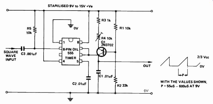
Fig. 31. Triggered linear-ramp generator can be used as the basis of an oscilloscope
time base.
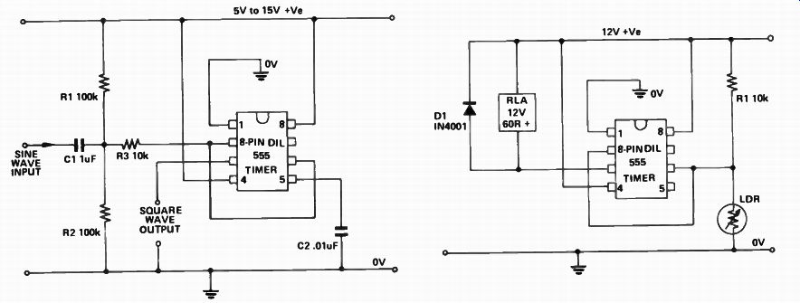
Fig. 32. 555 Schmitt trigger circuit acts as excellent sine/square converter
up to about 150 kHz.
Fig.
33. Dark-activated relay switch has built-in backlash.
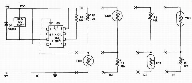
Fig. 34. Minimum-backlash relay switch can be activated by (al dark, (b) light,
(c) under- temperature, or (d) over- temperature.
If the circuit of Fig 31 is to be used as the basis of an oscilloscope timebase, note that the input driving signal must first be converted to a good square wave, from which suitable trigger pulses can be derived via C3 and R5. The minimum useful ramp period that can be obtained from the circuit is about 5 µS, which, when expanded to give full deflection on a ten-division ' scope screen, gives a maximum timebase speed of 0.5 4S-per-division. Flyback beam-suppression signals can be derived from the pin 3 OUTPUT terminal of the IC. The 'timebase' circuit gives superb signal synchronization at trigger frequencies up to about 150 kHz. If the timebase is to be used with input signal frequencies greater than this, the input signals should be divided down via a single- or multi decade digital divider. Using this technique, the timebase can be used to view input signals up to many MHz.
Figure 32 shows how a 555 can be connected for use as a simple but effective Schmitt trigger or Sine/Square converter.
The circuit acts as a good converter at input frequencies up to 150 kHz or more. It works by changing its output state each time the pin 2 input signal swings from above the 2/3 Vcc level to below the 1/3 Vcc level, or vice versa. Resistor R3 is wired in series with pin 2 of the chip to ensure that the input signal is not adversely influenced by the transition action of the IC. Figure 33 shows how the basic Schmitt circuit can be adapted to a dark-activated relay driving application by wiring light-dependent potential divider R1-LDR to the pin 2 input terminal of the IC. This circuit has an inherently high degree of input backlash, and is likely to be of value in only very specialized applications.
A far more useful relay-driving switching circuit is shown in Fig 34. This circuit has negligible input backlash, and can be used as either a light- or temperature- activated switch. In light- activated applications R1 is wired in series with a cadmium-sulphide photocell that presents a resistance in the approximate range 470 ohm to 10 k ohm at the required turn-on level. Dark-activated operation can be obtained by using the connections shown in Fig 34a or light-activated operation can be obtained by using the connections shown in Fig 34b.
For temperature-activated operation. R1 must be wired in series with a negative-temperature-coefficient thermistor, This thermistor must present a resistance in the range 470 ohm to 10 k-ohm at the required turn-on level. Under-temperature operation can be obtained by using the connections shown in Fig 34c, or over-temperature operation can be obtained by using the connections shown in Fig 34d.
1 kHz Analog Frequency Meter
This circuit needs a square-wave input driving signal with a peak-to- peak amplitude of two volts or greater. In this circuit the 555 is wired as a standard monostable multivibrator or pulse generator, and is powered from a regulated 6 V supply.
Transistor Q1 is used to amplify the square wave input signals to a level suitable for triggering the monostable stage, and the output of the monostable is fed to 1 mA fsd meter M1 via multiplier resistor R5 and offset-cancelling diode D1. This meter gives a reading that is directly proportional to the frequency of the square wave input signals, and its operating theory is as follows: Each time the monostable multivibrator is triggered it generates a pulse of fixed duration and fixed amplitude. If we assume that each generated pulse has a peak amplitude of 10 V and a period of 1 ms, and that the pulse generator is triggered at an input frequency of 500 Hz, it can be seen that the pulse is high ( at 10 V) for 500 ms in each 1000 ms total period, and that the MEAN value of output voltage measured over this total period is 250 ms/1000 ms x 10 V = 5 V, or 50% of 10 V. Similarly, if the input frequency is 250 Hz the pulse is high for 250 ms in each 1000 ms total period, so the mean output voltage equals 250 ms/1000 ms x 10 V = 2.5 V, or 25% of 10 V. Thus, the mean value of output voltage of the pulse generator, measured over a reasonable total number of pulses, is directly proportional to the repetition frequency of the generator.
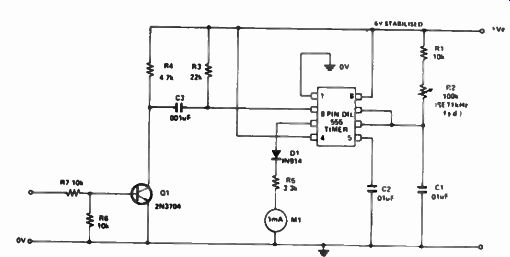
Fig. 35. Simple 1 kHz linear-scale analog frequency meter.
Normal moving coil meters are 'mean' reading instruments, and in the Fig 35 circuit a 1 mA fsd moving coil meter is wired in series with voltage multiplier resistor R5, which sets the meter sensitivity at about 3.4 V fsd, and is connected so that it reads the mean output voltage of the pulse generator. This meter thus gives a reading that is directly proportional to frequency, and the circuit thus acts as a linear-scale analog frequency meter. With the component values shown the circuit is intended to read fsd at 1 kHz. To set up the circuit initially, simply feed a 1 kHz square wave signal to its input, and then adjust R2 (which controls the pulse lengths) to give full-scale reading on the meter; all adjustments are then complete.
The full-scale frequency of the above circuit can be varied from about 100 Hz to about 100 kHz by suitable choice of C1 value. The circuit can be used to read frequencies up to tens of MHz by feeding the input signals to the monostable circuit via a single- or multi-decade digital divider, thereby reducing the input frequencies to values that can be read by the monostable circuit. The circuit can form the basis of an excellent and inexpensive multi- range linear-scale analog frequency meter.