Inherently rugged CMOS logic has many advantages over other logic families - high noise immunity and uncritical power requirements are but two. This new five-part series explains in practical down-to-earth terms just how CMOS should be used.
THE AVAILABILITY OF THE CD4000 series of chips brings CMOS to the forefront of logic technology to rival TTL in many applications. CMOS is far less critical as regards power supplies and possesses high noise immunity as well as capabilities which are not offered by other logic families.
In this series of articles we shall give various circuits which illustrate the use of CMOS. We suggest that these circuits can be 'breadboarded' on ETI Util-board (Aug 1975 issue) using DIL sockets - there is nothing like trying it to see.
Some of the circuitry, of course, is capable of realization in a number of different logic families, so that, in these cases, we will merely be introducing equivalents of familiar devices.
However, some of the applications we give show the major possibilities of CMOS.
---------------
TABLE 1
CMOS OPERATING LIMITS --- CD400A SERIES
STORAGE TEMPERATURE -65 to + 150 C
OPERATING TEMPERATURE -40 to +85 C
SUPPLY VOLTAGE LIMITS (VD D -Vss) -0.5 to + 15 V
PACKAGE DISSIPATION 200 mW max.
INPUT VOLTAGE Vss < Vin ,<V DD
RECOMMENDED SUPPLY VOLTAGE (V_DD - V_ss) +3 V to + 15
Unused inputs should be tied to a supply line. No input should be present when the supply lines are off.
--------------------
HANDLING AND USE
Firstly we shall deal with the disadvantages of CMOS and get these behind us before we look more closely at some of the virtues. The first point is that these devices are very susceptible to damage from surges of over- voltage from static electricity and unearthed test equipment. When you come to buy any CMOS ICs you should find them with their leads buried in foam. This foam is conductive and protects the device by putting all the pins together so do not remove it until the IC is to be put in circuit. If you run out of foam for storing devices then stick them into a piece of soft balsa wood. Whatever else you do, must not keep them in plastic containers or use ordinary plastic foam as this may develop a great deal of static. It is in fact a good rule to keep the devices away from all plastics as much as possible including any nylon clothing.
It is sensible to use IC sockets for the more expensive devices and also for any chip you may wish to re- use, but if you do solder them in solder the V_DD pin first, then Vss and then all the others.
The reason for this is that the common ranges of CMOS have internal protection devices which operate fully only when the supply lines are connected. While we are on the subject of soldering, check that your iron and any other instruments you may use (meters, oscilloscopes, etc) are all properly earthed.
The only other real disadvantages of CMOS compared with TTL are that it is slower ( typical gate rise time 25 nS) and that a few operating precautions are necessary.
Firstly, all unused inputs must go somewhere. The alternatives are tying unused inputs to used inputs, either to the supply line as appropriate, or to a supply line via a resistor ( 220 Id2 is usually about right). The latter solution is particularly helpful for inputs to which off- board connections are to be made. This avoids leaving the input "floating" until it is wired in. The other point is to ensure that the chips do not have signals at their inputs when the power supply is not on.
Now we shall consider a few of the advantages of CMOS. Most of these will come out more clearly later and so we shall just mention them briefly here.
The principal virtue is the ease of choice of power supply. This may be anywhere between three and fifteen volts at low current. The actual power required depends on operating frequency ( see Fig 1) being comparable with TTL at ten MHz but it is in the region of a few microwatts at sub- kilohertz speeds.
Voltage regulation is not required but operating speed and current consumption rise with increasing supply voltage. For most practical purposes CMOS will run off a nine volt battery or the simplest of mains power supplies.
Other advantages include high noise immunity and analog possibilities.
Before we proceed with some circuitry the table of operating conditions ( Table 1) should be studied. The limits shown in the table should be adhered to rigidly.
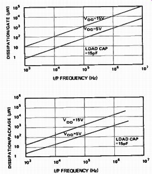
Fig 1. Power dissipation in CMOS as a function of frequency for a) a simple
gate and b) an MSJ package.
SIMPLE GATES
It is an unpleasant fact that it seems one must always start considering any subject at its least interesting parts and it is hardly surprising that the least interesting logic ICs are the simple gates.
We shall assume that the reader is familiar with truth tables and terminology and logic consequently our discussion will mainly be on the subject of monostable and astable multivibrators. For ease of future reference a list of basic CMOS gates and their pin-outs is given in Fig. 2. It is worth remembering that inverters may be realised by tying together all the inputs of a NAND or NOR gate, thus allowing a circuit requiring two NOR gates and two inverters to be constructed for a single type 4001A package.
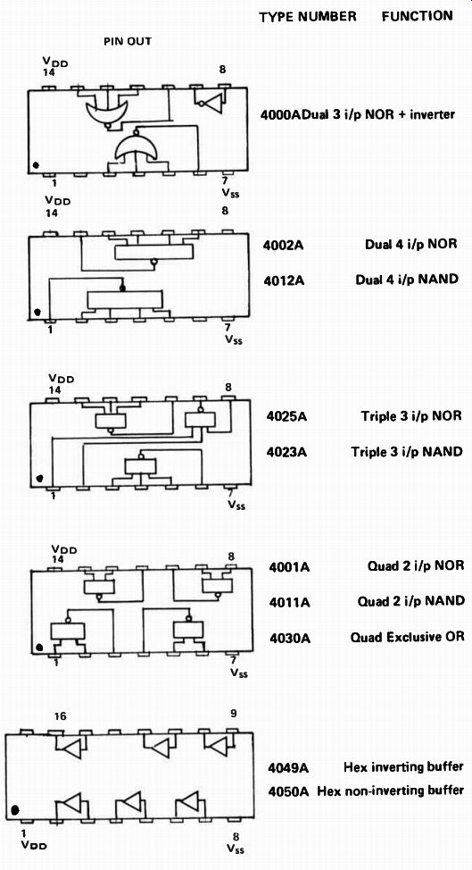
Fig. 2. Some simple CMOS gate packages.
ASTABLE MULTIVIBRATORS
The basic CMOS astable is shown in Fig. 3. This could of course be built using any of the packages in Fig 2 with the exceptions of the 4030A and 4050A, indeed, the 4049A could produce three of these circuits simultaneously. The period is approximately 1.4RC ( R in ohms, C in farads), and the waveform may have a non-unity mark-space ratio due to the voltage at which the inverters switch (called the transfer voltage - Vtr ) not being exactly half way between VDD and Vss. The frequency is also dependent on the supply voltage. In keeping with normal practice, connections of the device to the supply voltage have not been shown.
The next few circuits will rectify some of the aberrations of the simple version.
The addition in Fig. 4 of RA. which should be at least twice as large as R, makes the frequency almost independent of the supply voltage over a wide range. The frequency of any of the circuits may be made variable by making R a variable resistor.
Duty cycle adjustment may be achieved using the circuit in Fig. 5 Altering the duty cycle will affect the frequency and the diode may have to be reversed to achieve the desired result.
GATING
A gated multivibrator is shown in Fig. 6 where the oscillator only runs when the gate input is low, thus producing "bursts" of output in synchronism with the control signal. Using a NAND gate instead of the NOR would cause the circuit to run when the gate was high instead of low.
One of the huge advantages of CMOS is the very high input impedance. As a consequence timing resistors can be very large --- values in the hundred megohm region with capacitors of several microfarads can be a practical proposition.
Before we leave the astable multivibrator for a time we shall give one more circuit which corrects a tendency of all the preceding ones to "jitter" near the switching point. This requires an extra inverter and a fourth has been added as an output buffer.
There are also two inhibit inputs which stop the circuit with the output high or low, depending on which is used. The theoretical diagram is shown in Fig 7.
Another feature of this circuit, and indeed virtually all the others, is that the timing resistor may be substituted by one of the networks in Fig 8 to give a variable mark-space ratio. They work because the diodes effectively change the value of the timing resistor depending on whether the capacitor is charging or discharging, ratios as large as 5000:1 maybe used.
MONOSTABLE MULTIVIBRATORS
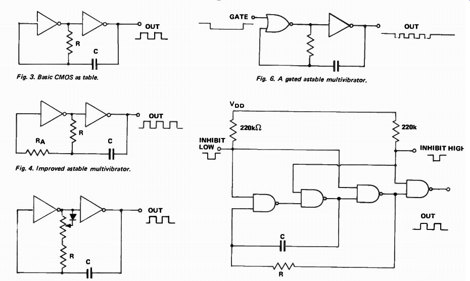
Fig. 3. Basic CMOS as table.
Fig. 4. Improved astable multivibrator.
Fig. 5. Duty cycle adjustment.
Fig. 6. A gated astable multivibrator.
Fig. 7. This jitter-free multivibrator (with inhibits) may be made from a 4011A.
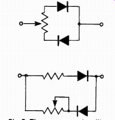
Fig. 8. These two networks will provide variable mark-space ratio for multivibrators.
The basic CMOS monostable is shown in Fig. 9. It is triggered by the input pulse's leading edge and produces a positive going output pulse. The period may vary by more than - ± 50% with different devices due to the dependence of the circuit on the transfer voltage of the inverter.
The circuit in Fig. 10 operates in an interesting way. The quiescent state is with the first and second inverter outputs at "0" and " 1" respectively. The falling edge of the triggering pulse makes the first inverter go high, C2 charges through the diode up to V_DD and the second inverter goes low thus initiating the output pulse. C1 recharges through R1 and crosses the transfer voltage of the first inverter which consequently goes low and is isolated from C2 by the now reverse- biased diode. Capacitor C2 then discharges through R2 and causes the second inverter to revert to its initial state, thus completing the output pulse. The advantage of all this is that inverters fabricated on the same chip have similar transfer voltages and if the two time constants ( R1C1 and R2C2) are made identical, errors cancel out and the period becomes well defined. It is in fact approximately equal to 1.4 R1C1 (= 1.4R2C2) and this circuit is capable of being retriggered during the output pulse.
Our last two monostables ( Figs.11/12) are non-retriggerable and the two time constants should be made the same as in the previous circuit. Figure 12 is particularly interesting because the circuit isolates the trigger input during the output pulse as the charge on C2 holds one input to the NOR gate high, thus keeping the output low independently of the state of the trigger input.
FREQUENCY DOUBLER
The frequency doubler shown in Fig. 13 works by differentiating the leading and trailing edges of the waveform and applying the resulting pulses to the two inputs of a NAND gate. This produces a complete output pulse at both the rise and fall of the input signal. The values of the discrete components will depend on the desired frequency of operation.
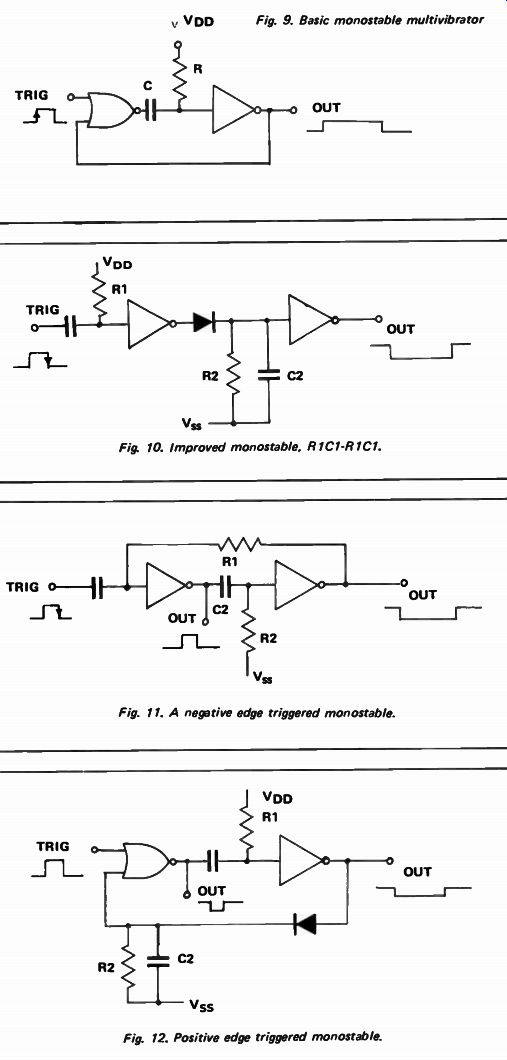
Fig. 9.-12 Basic monostable multivibrator OUT
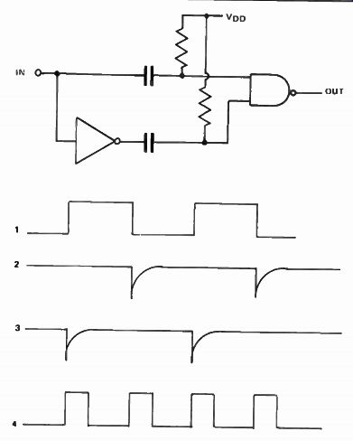
Fig. 13. Frequency doubler and associated waveforms.
THE 4007 The next device we are going to consider has no equivalent in other logic systems. It is described as a "dual complementary pair plus inverter" and its type number is 4007. It can perform several different functions and while we are discussing it we shall present a number of useful circuits and have the added advantage of learning a little about the internal operation of CMOS. In CMOS there are two different types of field-effect transistors, namely n-channel and p-channel enhancement mode devices ( see Fig. 14). What all this means is that when based in the conventional manner (drain positive in n-channel devices but negative in p-channel devices), the n-type turns on when the gate becomes sufficiently positive with respect to the source and the p-type when it is sufficiently negative. A "turned on" device may be considered to have a resistance of the order of 500 ohms - 1k between source and drain whereas the equivalent resistance when "off" is about 10^9 ohms . The resistance at the gate is always very high (> 10^12 ohm) regardless of tile state of the device.
The working of the CMOS inverter (Fig. 15) should now be fairly clear.
When the input is "high" the bottom FET is turned on and the top one off.
Thus the output voltage is held very low. When the input is low the FETs reverse roles and the output is high.
Now look at Fig. 16 which shows the internal circuitry of the 4007. You should be able to see how joining a few pins together will allow three separate inverters to be produced. Reference to Fig. 17 will reveal how several other gates may be produced and their mode of operation should be relatively easy to discern.
TRANSMISSION GATES
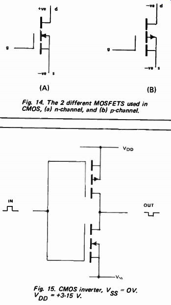
Fig. 14. The 2 different MOSFETS used in CMOS, (a) n-channel, and (b) p-channel.
Fig. 15. CMOS inverter, V ss = 0V. VDD = +3-15 V.
There is another way of connecting two FETS which produces a result unique to CMOS. This is the transmission gate ( Fig. 18). Here, due to the inverter, both FETS are either on or off simultaneously. When they are on, the path between input and output (they are interchangeable) may be regarded as a resistor of about 500 ohms - 1k-o whereas when they are off the equivalent value is about 1000 M-o. Thus the device behaves as a switch capable of passing analog signals with very little distortion provided that the load resistance is fairly high 100 k-o). We shall have more to say about these "bilateral switches" later but while we are dealing with the 4007 Fig. 19 shows how to connect one as a single pole-double throw switch which will pass analog signals in both directions.
Any of the three or less inverter circuits we have mentioned to date may be realised with a 4007, as may several more interesting designs. Figure 22 shows a linear frequency-to-voltage converter which works by charging a capacitor once for every input cycle, the charge to do so being passed by a MOSFET into a summing amplifier. The component values given are based on an approximate five volt output for the given frequency. The resistor R1 should be made a 100 k- ohm preset if it is required to set a range exactly. The capacitor C2 "smooths" the output and need not be changed from 10pF if fast response on the upper ranges is not needed. The linearity achieved on the top range will depend on the particular "741" used and if reliable operation is required higher speed op-amp should be used.
Figure 21 shows an alternative monostable multivibrator. We have already given a number of multivibrator circuits and so we shall say nothing more about this one except that it has an extremely small power consumption.
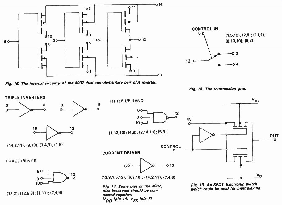
Fig. 16. The internal circuitry of the 4007 dual complementary pair plus inverter.
Fig. 17. Some uses of the 4007; pins bracketed should be connected together.
Fig. 18. The transmission gate.
Fig. 19. An SPDT Electronic switch which could be used for multiplexing.
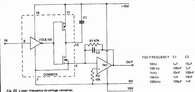
Fig. 20. Linear frequency- to-voltage converter. 15V
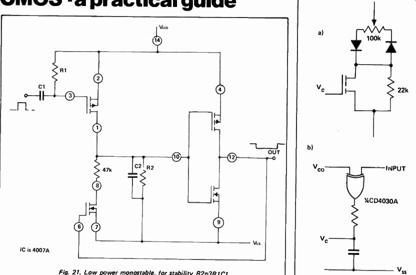
Fig. 21.
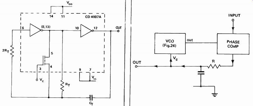
Fig. 22 A voltage controlled oscillator using the 4007 1C.

Fig. 23. Outline of PLL receiver.

Fig. 24. (al Adjustable M-S ratio narrow range controller, (b)
Exclusive- OR phase comparator.
This is due to the feedback connection (pins 12-6) which turns off the n-channel MOS-FET during the discharge of the time constant. This circuit is also an interesting demonstration of the use of components in the 4007 as discrete transistors.
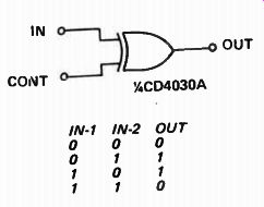
Fig. 25. Exclusive- OR gate used as a conditional inverter together with the
device's truth table.
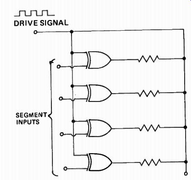
Fig. 26. Exclusive-OR gates driving liquid crystals segments, represented
by resistors.
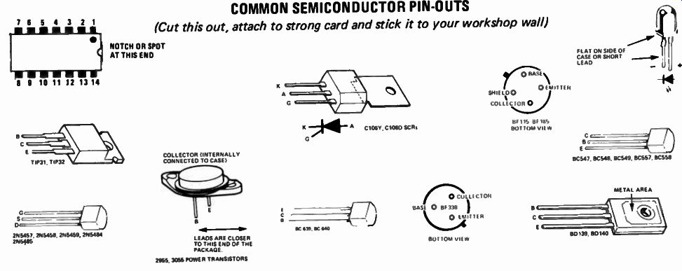
------ COMMON SEMICONDUCTOR PIN-OUTS (Cut this out, attach to strong
card and stick it to your workshop wall)
A WIDE RANGE VCO
The voltage controlled oscillator shown in Fig. 24 uses two inverters as well as a separate transistor as a voltage controlled resistor. The inverters function as an astable multivibrator in the manner of Fig. 4 but the timing resistance is the parallel combination of R T and the FET. As V, varies between Vdd and V„ so the resistance of the FET varies between about 1 k and 1000 M-o. If the upper value is limited to 10 M-o.), by making Rt that value, then the circuit will sweep over a 10000:1 range in frequency. There would seem to be scope here for experimenting with a pulse frequency modulation communications system.
One might produce an analog system although distortion would probably be high due to mismatching. The transmitter could be the circuit in Fig. 22 and the receiver a phase locked loop along similar lines ( Fig. 23) using some sort of phase comparator and a low-pass R-C filter.
EXCLUSIVE- OR GATES
Exclusive-or gates, for example the 4030 (see Fig. 2), will function as phase comparators but they require a unity mark-space ratio to be effective. Perhaps a voltage controlled oscillator might be designed with a narrower range along the lines of Fig. 24 for both transmitter and receiver, together with a phase comparator and low pass filter as shown in Fig. 24. While we are on the subject of the exclusive-or function we shall consider two more uses of these devices.
Figure 25 shows the exclusive-or truth table and its use as a conditional inverter. This configuration causes the input signal to be inverted when the control input is high but not when it is low.
Liquid crystal displays are undoubtedly the readout devices of the future but they last longer in general if ac drive is used. If then a square wave is applied to one end of a liquid crystal segment and also to the other connection via a conditional inverter (see Fig. 26) then the control input will decide whether or not there is a net voltage across the segment.
CMOS and liquid crystal make an ideal combination for ultra- low power logic and display systems and so manufacturers have produced BCD-to-seven-segment decoders and drivers specifically for this application.
Their type numbers are 4054/5/6, the variations being due to the addition of latches and other refinements. These devices have too limited an appeal to justify a full description here.