In the previous Section the basic theory of the operation of FM transmitters was discussed. Different types of modulator systems were studied as well as the theory underlying the need for frequency multiplication. The original Armstrong system was also analyzed to familiarize the reader with the first type of so-called FM transmitter that the FCC allowed to operate. These topics should have inculcated a fairly good idea of how FM transmitters operate. Section 4 will consider a number of different transmitters that are in operation today. Included in this group will be the commercial stations that operate on the broadcast band (wide-band FM) and other transmitters, such as police and ham sets, that operate on the narrow band.
This reference to wide band and narrow band is with respect to the amount of frequency deviation employed. In the transmitters to be discussed the type of modulation employed differs for different sets.
For instance, in the Armstrong transmitter indirect FM is used (initially starts with p.m.), in the Federal and RCA transmitters direct FM is used, and in some police and ham equipment indirect FM is used.
Discussion of these various different transmitters will introduce new subjects, heretofore not analyzed. To comprehend fully how the numerous different types of transmitters operate, many of these new topics will have to be studied, among them frequency division, pre emphasis, motor frequency control, audio correction (pre-distortion), and balanced modulators. Analysis of these topics will be included with the discussions of the different transmitters. For instance, the topic of audio correction or balanced modulators will be discussed in conjunction with the Armstrong system. This does not mean, however, that a particular topic is concerned only with the transmitter under discussion. Audio correction networks and balanced modulators, for example, may also be employed in other transmitters that use phase shifting to obtain the final required FM signal. This should be kept in mind throughout this Section.
Analysis of the different FM transmitters in operation today is going to be made by comparison, wherever possible, of their construction on the old FM band and on the new FM band. It should be remembered that the old FM band was between 42-50 mhz and the new band between 88-108 mhz.
1. Discussion will center about the exciter unit and frequency control systems (if any) of the main transmitter. Although the change over from the old to the new FM band is an increase in frequency of approximately two to one, the purpose was not at all to increase the frequencies of all stations by exactly twice the old frequency. Consequently, there had to be a number of changes, including the master oscillator and frequency multiplication stages.
All this will be seen as the Section progresses.
Audio Correction
Under the discussion of the Armstrong transmitter in Section 3, it was stated that in order to have the p.m. directly tantamount to FM, the amount of phase deviation had to be independent of the frequency of the audio modulating signal. To accomplish this the audio input frequency to the system had to pass through an audio correction net work, sometimes known as a pre-distorter. Essentially, the effect of this correction network was to make the ratio of output amplitude to its input amplitude inversely proportional to the audio frequency.
Since the phase deviation that would ordinarily occur, without correction, would be a function of the audio frequency, call it f, then with the correction network inserted, the output audio frequency (to the balanced modulator in this instance) is proportional to 1/f. Consequently, it is seen that the effect of the audio frequency upon the amount of phase deviation is canceled by the correction network. The amount of phase deviation of the p-m signal is not affected by the frequency of the audio signal, but by its amplitude only, which is exactly what happens in direct FM
To explain this in somewhat greater detail let us consider the simple audio correction network as illustrated in Fig. 4-1. The circuit is nothing more than a simple RC series network in which the output voltage is taken across the capacitor C. Across terminals A, B is impressed the audio frequency voltage E. Due to the impedance of the circuit, a series current I is caused to flow through R and C. If the resistance of R is made much larger than the reactance of C for all audio frequencies involved (down to 50 cycles), the current deter mining component is primarily R, and the reactance of C has negligible effect on the amount of current flow. Since this is so, it can be said...
[1. Of this new 88-108 mhz band the frequencies between 88 and 92 mhz are allocated for educational FM, those between 92 and 106 mhz are allocated for commercial FM, and those between 106 and 108 mhz for facsimile.]
that the current flowing in the series circuit is primarily dependent upon Rand we can write from Ohm's law that: E l=R
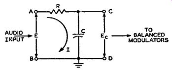
Fig. 4-1. A simple audio correction network, consisting of an RC series
network in which the output voltage is taken across the capacitor C.
Since the reactance of Chas negligible effect on I, the frequency of the audio voltage also has negligible effect on the amount of current.
It is only the reactance of an a-c circuit (if any), whether it be inductive or capacitive, not the resistance, that changes with frequency.
Therefore, the element in this circuit that changes with frequency is the capacitive reactance, but, since the magnitude of this reactance is very small as compared to R, its effect on the amount of I can be neglected. In this respect the current I is said to be independent of the frequency and primarily dependent upon Rand upon the magnitude of E, as indicated in the above relation.
Now the amplitude of the voltage Ee appearing across the capacitor C (across terminals C, D) is applied to the balanced modulators and is supposed to be inversely proportional to the frequency of the modulating signal. By the prearranged condition that R be much greater than the reactance of C, this is possible. This is simply proved by the following mathematics: The voltage E0 across the capacitor is, by Ohm's law, equal to the current flowing through the capacitor multiplied by the reactance of the capacitor. The reactance of a capacitor, designated as Xe, is inversely proportional to frequency and in exact terms is; Xe = 2 pi C in ohms where X0 is the amount of capacitive reactance in ohms f the frequency of operation in cycles per second C the capacity in farads ,r a numerical quantity equal to 3.14.
The voltage Ee is then equal to the current I multiplied by X0, or to be more concise: I Ee= 2 pi fC In this last expression the current I is the same current I as in the first equation, where I = E/R, (because it is a series circuit and in such a circuit the current throughout is always the same) and by substituting the expression for I from the first equation into the last one, we find: E/R E Ee = 2 pi fC = 2 pi f CR
Since 2 pi CR is a numerical constant (1T, C, and R have predetermined values) we can call this constant by the letter K and rewrite the foregoing as E Eo=Kf From this last equation it is readily seen that the voltage E0 across the capacitor C (that applied to the balanced modulators) is directly dependent upon the amplitude of the incoming audio voltage E and inversely proportional to the frequency f of the audio signal. Thus, the required prerequisites for the amount of p.m., being independent of the audio frequency, have been attained by making the voltage input to the modulators proportional to 1/f (that is, inversely proportional to f.) This type of circuit is also referred to as a pre-distorter network because it distorts the frequency response curve of the input to the modulators that would be present if the corrective network were not there. In the case of a true speech or music signal, which is a complex audio wave, the ratio of distortion between the harmonics and the fundamental frequency is such that the fractional reduction follows the number of the harmonic.
The output of the correction network is often fed into a linear amplifier, because there is a loss in gain when going through this correction network.
Balanced Modulators
A balanced amplitude modulator, as previously mentioned, serves the purpose of producing in its output circuit only the double side band portion of the modulated input r-f signal. Numerous different types of circuit arrangements can produce the desired double side band. This output containing the intelligence can then be shifted in phase and recombined with the carrier signal, effectively producing a new signal that is phase modulated.
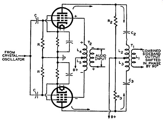
Fig. 4-2. Schematic of the balanced modulator circuit used in the original.
Armstrong FM transmitter.
As an illustration of the operation of a typical balanced modulator (tube modulator) let us consider the balanced modulator circuit as used in the original Armstrong transmitter. The schematic for this modulator circuit is shown in Fig. 4-2. Since both the old and new FM bands are in operation. Armstrong devised a dual system where the same crystal oscillator and balanced modulator is simultaneously used to operate on both bands. This will be more evident in the next section. Let us consider the balanced modulator circuit of Fig. 4-2 without any audio input signal applied to the screen grids to see how this system balances out the carrier frequency. The input control grids are effectively connected in parallel, through similar RC networks.
Some of the output from the crystal oscillator is applied to the control grids of each modulator tube. The circuit is so arranged that the same amount of oscillator voltage at the same phase is applied to each grid.
With the necessary equal supply voltages on the tubes, equal plate current will flow in each tube. With the same polarity on the individual grids, the polarity (or phase) of the signals on both plates is also in phase but shifted, of course, 180 degrees from that of the signal on the grid. The plates (that is, outputs) of the tubes are connected in push-pull through the primary of transformer T1. This means that the plate signal currents will flow in opposite directions as indicated by the arrows in Fig. 4-2. This is exactly opposite to what happens in a regular push-pull power amplifier circuit where the grids, however, are in push-pull and receive out of phase but equal voltages, making the plate polarities of opposite phase. Flowing in opposite directions in the balanced modulator circuit, the plate currents when combined induce no voltage into the secondary coil L1 of transformer T1. This is fully explained as follows: The signal plate current from the upper modulator tube flows through the L, part of the split primary of transformer T1 and sets up a varying magnetic field in accordance with the crystal oscillator frequency. The signal plate current from the lower modulator tube flows through the L8 part of the primary of the same transformer. The current flowing through L8 also sets up a varying magnetic field in accordance with the oscillator frequency. This current, however, is flowing in the opposite direction to the previous current, which means that this magnetic field is varying in an opposite manner to the other field. Since the primary of the transformer is center-tapped and since the signal plate currents are equal in magnitude and of the same phase, the effect of the two varying magnetic fields is such that they cancel each other. They induce equal voltages across the secondary of the transformer, but these voltages have opposite polarities and cancel each other whereupon no voltage appears across the output terminals of the secondary. We have just seen how the balanced modulator tubes will function with respect to just a carrier frequency signal applied to its input control grids. Under this condition of operation it is found that no signal appears in the output circuit at all, which means the unmodulated carrier frequency was suppressed.
The balanced modulator circuit is very critical. If any unbalance exists in the circuit such that the plate currents flowing from both tubes (with no audio applied) are not equal, then some of the carrier frequency will appear in the output circuit, because the varying magnetic fields do not quite cancel each other. Consequently, both modulator tubes have to be as nearly equal in tube characteristics as is possible. Also the voltages supplied to both tubes have to be exactly the same. This includes both d-c supply voltages and the input crystal oscillator signal.
From this same diagram of Fig. 4-2, but with the audio input circuit connected as shown, we can determine how the double sideband component alone is obtained and shifted in phase by 90 degrees.
We have an audio input transformer, T2, so arranged that the secondary is center tapped with the tap going to B+. The other terminals of the secondary are respectively connected to the screen grids of both modulator tubes. When an audio signal is applied across the primary of the transformer, equal voltages are applied to the screen grids due to the center-tapping of the secondary. The crystal oscillator frequency, already impressed across the control grids, causes r-f current to flow in the plate circuit, and the audio signal impressed on the screen grids amplitude modulates this plate current at the audio frequency. Thus, initially the system starts with AM The audio trans former is connected push-pull to the screen grid which means that, although the signal voltages applied to these grids are of the same value, they are of opposite polarity. This is the same type of situation that exists in a push-pull amplifier stage which uses a transformer input to obtain the necessary phase inversion. Consequently, the audio signal causes an unbalance between the two modulator tubes, and, as mentioned before, any unbalance in the system causes a voltage to appear across the secondary of the output transformer T1. If the tubes are perfectly balanced as far as everything except the audio signal is concerned, the audio signal will be the only cause of unbalance, and the output voltage across the secondary of T1 will contain a signal that is varying in polarity and amplitude in accordance with this audio signal. This is more fully explained as follows: Assume that for one-half cycle of audio the polarity on the terminals of the primary of T 2 is indicated by the plus and minus marks in Fig. 4-2. Since by transformer action the signal induced in the secondary, from the magnetic field caused by the primary, is 180 degrees out of phase with the primary signal, the polarities across the secondary will be as indicated. Thus, according to the polarity of the primary, the polarity across the secondary is such that the top of coil L4 is more positive than the bottom of L5. This means that for the half cycle of signal input under discussion, the voltages on the screen grid of the upper tube will be more positive than that voltage on the screen grid of the lower tube (indicated by the positive and negative signs respectively.) On the other half cycle of the audio signal input, the polarities between the two screen grids reverse, with the lower screen grid becoming more positive with respect to the voltage on the upper screen grid. In either half cycle the system is thrown out of balance as a result of unequal voltages on the screen grids. The audio signal then amplitude modulates the r-f plate currents and in the output of the system appears an a-m signal.
[It should be remembered that the amount of AM is very slight in order to have the a-m sidebands of the correct strength, so that the p-m signal to follow will have negligible amplitude variations.]
In the output circuit of the system of Fig, 4-2 are two series resonant circuits; capacitor C, in conjunction with inductance L, and capacitor Cs in conjunction with inductance L8. Both form series resonant circuits which are broadly tuned to the crystal oscillator frequency. The tuning of each series tuned circuit is made broad by the resistors R, and Rs that are in parallel across each series circuit. The tuned circuits are made broad enough so that they will be selective to both sideband frequencies as well as the center frequency. Since the tuned circuits are in series resonance, they will offer a minimum amount of impedance to the tuned frequency, and, consequently, most of the r-f plate current will flow in the directions indicated in Fig. 4-2 with very little through R2 and Rs, The plate currents, now being slightly amplitude modulated, consist of a center frequency component and two sidebands, an upper and a lower. The center frequency component of the a-m signal is at the frequency of the crystal oscillator, and it has been shown how, with the system in balance for the crystal oscillator frequency, this frequency is suppressed. This also happens to the center frequency component of the a-m wave, and, consequently, all that is left is the two sidebands which combine into the double sideband in T1.
These sidebands contain the audio intelligence, and, therefore, vary at a rate determined by the audio signal. Because this audio signal creates an unbalance in the modulator tubes, the double sideband component of plate current in one tube will at one-half cycle of audio form a magnetic field about its half of the primary of T1 with its north pole towards the center tap. The signal current in the other tube will produce a magnetic field with its north pole away from the center tap.
Thus, the fields are effectively in series, aiding one another, and a voltage of double sideband frequency will be induced into the secondary of T1. The strength of this voltage depends upon the strength of the two r-f plate currents, which in turn cause magnetic fields about the individual halves of the primary of T1, On the other half cycle of audio, the situation is reversed, and the magnetic fields point in the opposite direction. This causes a double sideband signal to be impressed across the secondary of T1 as before.
Thus, the balanced modulator system produces only the double sideband signal of an a-m wave. As has been stated, this double side band has to be shifted in phase by 90° and then recombined with the crystal carrier signal to obtain the necessary slightly modulated p-m wave which is equivalent to a slightly modulated FM wave as deter mined by the audio correction network. The next problem is shifting this double sideband in phase by the required 90°. This phase change takes place in the output transformer T1. (It is often referred to as the phase shifter.) Before the voltage is induced into the secondary of T1, the double sideband component that produces the magnetic field about the primary of the transformer is an exact component part of a true a-m wave with respect to phase. The use of some vector diagrams will make it easier to understand how the phase change from primary to secondary comes about. In an untuned transformer, the voltages in the primary and secondary are 180° out of phase. While in any inductor the current lags the voltage by 90°. In Fig. 4-3 (A) the primary current IP is seen to lag the primary voltage Ep by 90°. It is also known that the secondary induced voltage E, lags the primary current Ip, that causes the induced voltage, by 90° and this is likewise shown in Fig. 4-3 (A). This means that the current 18, caused by the induced voltage E., lags this voltage by 90°, because the secondary is an untuned inductance This means that the currents in the primary and secondary, as well as the voltages in the primary and secondary, are 180° out of phase with each other. All this is vectorially illustrated in Fig. 4-3 (A).
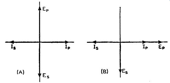
Fig. 4-3. Vector diagrams of the voltage and current relationships of
an untuned transformer (A) and output transformer (B) of balanced modulator
circuit shown in Fig. 4-2.
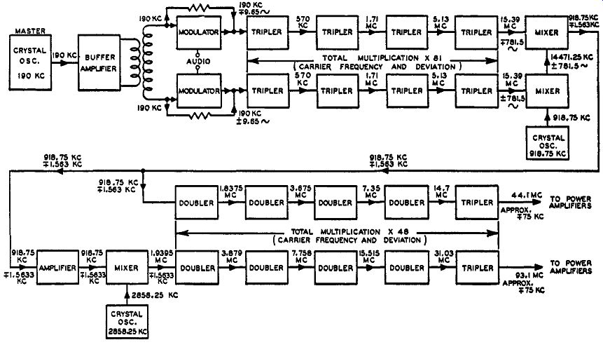
Fig. 4-4. Block diagram of Armstrong "dual channel" transmitter.
With these phase relations established, let us refer back to the output transformer of the balanced modulator circuit of Fig. 4-2. Since the primary of the transformer is series tuned ( as previously discussed) it offers a purely resistive impedance to its broad resonant frequency. This means that the current and voltage in this primary circuit are in phase with each other. This is shown vectorially in Fig. 4-3 (B) where Ip and EP are the respective primary current and voltage. As in the case of the untuned transformer, voltage E8 induced in the secondary lags the current flowing through the primary by 90°, as indicated by the respective vectors. From this vector diagram it is consequently seen that the voltage induced across the secondary is 90° out of phase with primary voltage Ep. Thus, we have established the fact that the output transformer T1 having a tuned primary as indicated in Fig. 4-2 and an untuned secondary causes a phase shift of 90° between the voltage in the primary and secondary. (The actual change is such that the secondary voltage E8 lags the primary voltage by 90°.)
Hence, since the double sideband is the only component appearing in the output circuit. it is shifted in phase by 90° because of the inherent phase relations of the output transformer circuit. This double sideband is then combined with the crystal carrier frequency, and the combination is such that the resultant signal is varying in phase and amplitude as indicated in the vector diagrams of Fig. 3-19. If the amplitude variations in the resultant signal are made to have negligible effect (accomplished by producing a slightly a-m signal to start with so that the amplitude of the phase-shifted double sideband components is very small compared with the amplitude of the carrier), the resultant signal is effectively varying only in phase. Due to the nature of the audio correction network, the relationship of the phase change is such that the resultant signal is equivalent to a frequency-modulated wave.
ARMSTRONG "DUAL CHANNEL" TRANSMITTER
The characteristics of the original Armstrong transmitter and the accompanying circuit discussions are considered necessary, because they were the original circuits upon which the basic foundation of AM to p.m. to FM was built. The Armstrong transmitter, as in use today, employs a similar technique of indirect FM transmission, but the circuit is quite different. At the time of this writing both the old and the new FM bands are in operation. To make sure that those radio receiver sets tuned to the old band receive FM signals, as well as those radios designed for the new FM band, the Armstrong transmitter at Alpine, N. J., as well as some other stations of today, works simultaneously on both bands. In this transmitter arrangement the Armstrong dual channel phase shift modulator is employed. The modulator is still energized by a crystal controlled oscillator and the modulation process is still from AM to p.m. to FM This dual modulator system, however, produces desired effects which were not avail able with the original system.
Before discussing the modulator system let us first study the complete transmitter as operating on both FM bands from a block dia gram view. Fig. 4-4 is a block diagram of the Armstrong "dual channel" transmitter as operated on both bands. The frequency of trans mission on the old band is 44.1 mhz, and on the new band 93.1 mhz. To comprehend how the system functions to produce both frequencies of transmission simultaneously, it will be best to analyze the block dia gram from the beginning of the circuit and trace the path of the signal.
The frequency of the crystal oscillator is 190 khz, and this signal is impressed across a buffer amplifier stage before it is applied to the dual modulator system. The dual modulator system, which also has an audio signal injected into it, functions in such a manner that a p-m signal appears in the output of both modulator tubes. This p-m signal has a peak phase deviation of 11.06° as compared with the peak deviation of 75- khz output from the transmitter proper (for 100 percent modulation) for a minimum audio frequency of 50 cycles. (As pointed out before, this is for a final output of less than one percent distortion.) The equivalent frequency deviation, for this amount of phase deviation, at 50 cycles of audio is equal to 9.65 cycles. This may sound like a very small figure in conjunction with the 190- khz crystal oscillator frequency, but when the small amount of allowable distortion output is taken into account, this frequency deviation is considered to be good. The necessary amount of multiplication in conjunction with a double conversion system brings the original peak deviation up to the necessary 75 khz. This will soon be evident. The upper part of the block diagram (above the horizontal center line) is used on both bands, whereas the lower part has one section devoted to the old band and one to the new.
The modulator circuit is so arranged that, although the FM outputs are the same, the deviations are out of phase with each other. This means that, if the input to the upper tripler section is such that the frequency deviation first swings in a decreasing direction, the frequency swing of the input to the lower triplers will be in an increasing direction. In other words, when the frequency swing of the FM signal to one tripler section makes the instantaneous frequency of the FM signal a minimum, the frequency .:;wing of the FM signal to the other tripler section makes its instantaneous frequency a maximum. As a result, the frequency deviations of the FM signal input to the triplers are of opposite polarity at any one instant of time. This is indicated by the polarity markings next to the peak frequency deviation values accompanying the carrier frequency component in Fig. 4-4.
What we now have at the input to the tripler sections is the same center frequency component of the FM signal, but the peak frequency swings are of opposite polarity. If we send these FM signals through a series of separate multipliers, the peak frequency deviation will be multiplied by the same amount as the center frequency component. In this transmitter there is employed a dual chain of .four tripler multiplication stages into which each individual FM signal output from the modulators is injected. The total multiplication of the four tripler multiplication stages is 3 X 3 X 3 X 3 or 81 times.
Thus, at the output of the last tripler in each chain the center frequency component of the FM signals will be 190 khz multiplied by 81, or 15.39 mhz, from both dual channels, since the frequency input to the first triplers is 190 khz. The values of the individual center frequency components of the FM signal before they enter the different triplers are indicated next to the arrow showing the direction of flow.
The frequency deviation is also multiplied 81 times, and with the original peak deviation equal to 9.65 khz, the output peak deviation from the last tripler of each multiplication chain will be 781.5 cycles.
Throughout the process of multiplication the polarity difference between the two separate frequency deviations is maintained, the separate deviations being 180° out of phase with each other. This is indicated by the polarity signs accompanying the 781.5-cycle markings on the block diagram of Fig. 4-4.
Next to be treated is one of the most important parts of this dual channel system of frequency modulation - namely the double con version system which has the purpose of doubling the frequency deviation and producing a new center frequency component. The outputs from both tripler chains are injected into separate mixer stages. To secure stability of the new center frequency, a crystal oscillator is used which operates at a frequency of 918.75 khz. The output from this crystal oscillator is injected only into the lower mixer of the system.
Conversion takes place inside this mixer stage and, due to the selectivity in the output circuit of the mixer, the output frequency is equal to the FM signal frequency less the crystal oscillator frequency.
Therefore, we have 15.39 mhz less 0.91875 mhz which is equal to 14.47125 mhz. This output FM signal, which still has the same amount of frequency deviation ( this was discussed in the preceding Section), is injected into the upper mixer stage.
Let us realize something at this moment. The lower mixer stage had an FM signal and an unmodulated carrier signal injected into it with the result that the new signal is still frequency modulated and lower in value but with the same deviation frequency as the original FM signal input. The upper mixer tube has two FM signals injected into it, one from the previous mixer and the other from the last tripler stage of the upper multiplier system of the dual channel arrangement. The task of conversion in this mixer tube is somewhat different. The selective circuit in the output is such that the difference frequency between the two FM signals is selected. The upper frequency ( center frequency components of course) is 15.39 mhz and the lower frequency 14.47125 mhz, and the difference between these two signals is equal to 918.75 khz, the exact frequency of the crystal oscillator used in the first conversion circuit. Thus, the output frequency from the double con version system does not depend upon the 190- khz master crystal oscillator frequency, but rather upon the crystal frequency of the conversion system, so that the master crystal frequency does not have to be exactly 190 khz but can vary somewhat on either side.
The really important feature of this double conversion system is the relationships of the individual frequency deviations of the two FM signal inputs to the upper mixer tube. As is known, these frequency deviations are of opposite polarity (input to the multiplier chains), but the amount of deviation in each case is the same-781.5 cycles.
Calling the FM signal input from the tripler to the top mixer f and the other FM signal input from the bottom mixer to the top mixer f1, the frequency output will be f - ft. The frequency off is equal to a 15.39 mhz center frequency component and also a 781.5-cycle peak deviation.
The frequency f1 is equal to a 14.47125-mhz center frequency component and also a 781.5-cycle peak deviation. If, at any one instant of time, the frequency deviation of f advances to a maximum positive value, the frequency deviation of f1 will advance to a maximum negative value. With this in mind, let us perform the subtraction off - f 1 to obtain the output FM signal from the mixer at the instant that the peak deviation of f is swinging in the maximum positive direction.
Therefore, we have 15.39 mhz-14.47125 mhz = 918.75 khz for the center frequency component, and for the frequency deviation we have: (781.5 cycles) - (-781.5 cycles) = 781.5 + 781.5 = 1.563 khz.
This indicates that at the instant of time indicated, the actual frequency swing of the output FM signal from the top mixer is equal to twice the original deviation.
Considering the peak deviation swing of f at the moment it is in the maximum negative direction means that the peak deviation swing of f1 is in the maximum positive direction. If we still perform the mixer function of f-f1, we find that the center frequency component does not change but that the deviation will be: (-781.5) cycles- (+781.5cycles) =-1.563 khz.
This indicates that at the other extreme end of the peak deviation of the FM signal inputs to the mixers, the peak deviation of the FM signal outputs from the conversion system is still twice the original deviations, but in a negative direction.
The final outcome of this double conversion system is to produce a new FM signal that has a different center frequency component equal in value to the crystal oscillator frequency employed in the conversion system, and also to double the frequency deviation that occurs at the output of the last tripler stages. The new signal output from the double conversion system is al' FM wave that has a center frequency component equal to 918.75 khz and a peak deviation equal to 1.563 khz.
From here, this FM signal is split up for transmission on the two separate bands.
Two individual channels are provided for this, as shown in the bottom part of the block diagram of Fig. 4-4. One produces the frequency output of 44.1 mhz on the old band and the other produces the frequency output of 93.1 mhz on the new band. Analysis of these two channels is very simple. Part of the FM signal output of 918.75 khz with a peak deviation of 1.563 khz is passed directly through a new chain of multiplier stages to produce the 44.1 -mhz output for the old band. To obtain this 44.1 -mhz output in conjunction with the necessary 75- khz peak frequency deviation it is found, if we divide 44.1 mhz by 918.75 khz, that the amount of multiplication needed will be 48. Likewise, dividing the peak deviation of 75 khz by the peak deviation of 1.563 khz it will be found that the amount of multiplication needed is also 48.
Consequently, the chain of multipliers into which part of this new FM signal is injected, has a multiplication of 48. To secure this multiplication four doubler stages, from which a multiplication of 16 is obtained (2 X 2 X 2 X 2 = 16), and a tripler stage are used, thus 16 X 3 = 48.
If we multiply 918.75 khz by 48, the frequency found will be equal to 44.1 mhz, and if we multiply 1.563 khz by 48, the peak deviation found will be equal to 75 khz. From the output of these multiplier stages the signal is applied to the necessary power amplifiers and antenna. Thus, it is easily seen how the intelligence is conveyed on the old FM band.
The other part of the 918.75- khz signal that is taken off the double conversion system is applied to the second channel, namely that one producing the 93.1-mhz signal for the new band. Since the maximum amount of peak frequency deviation must remain the same on- both bands and since the initial amount of peak deviation is still equal to 1.563 khz, the same amount of frequency multiplication of 48 has to be employed in this system to insure the final 75- khz deviation output.
Therefore, the multiplication system consists of four doublers and one tripler the same as for the old band. However, the center frequency component has to be much greater than 918.75 khz in order that a multiplication of 48 increase this frequency component to 93.1 mhz.
This is accomplished by a single conversion system.
This part of the 918.75- khz FM signal from the double conversion system is first sent through an amplifier stage to increase its strength.
Afterward it is injected into a mixer tube along with an external signal from a crystal oscillator whose frequency is equal to 2858.25 khz.
It is known, from the analysis of the double conversion system and Armstrong's original transmitter, that, when an FM signal and an unmodulated carrier are mixed together for the process of conversion, the frequency deviation of the FM signal remains unchanged. With the output circuit of the mixer tuned to the difference frequency between the two input signals to the mixer, the signal output will be equal to 2858.25 khz minus 918.75 khz, or 1.9395 mhz. Thus, the FM signal output from the mixer stage will have a center frequency component equal to 1.9395 mhz but a peak frequency deviation still equal to 1.563 khz. This signal then enters the multiplication stages in which the 1.9395 -mhz signal is multiplied 48 times to give a center frequency output of 93.1 mhz, and, as mentioned before, the 1.563- khz deviation is multiplied 48 times to give the 75- khz deviation output. After the multiplication stages, the output FM signal is applied to the necessary power amplifiers and antenna for transmission. The power amplifier stages and antenna are separate circuits for each frequency of transmission.
Dual-Channel Phase-Shift Balanced Modulator
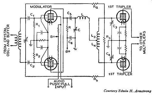
Fig. 4-5. Schematic diagram of the dual-channel phase-shift balanced
modulator used in the present Armstrong transmitter.
The heart of the Armstrong transmitter of today is the dual channel phase-shift balanced modulator. In discussing the block diagram of the Armstrong transmitter we passed lightly over the modulator system merely stating the character of the output signals without revealing how they were obtained. The reason was that this analysis is quite intricate compared with the rest of the system and therefore requires a more detailed discussion.
The schematic diagram for this modulator system is shown in Fig. 4-5. Only two tubes are used for the modulators, similar to the original Armstrong balanced modulator circuit. In the newer system, however, the analysis is quite different and entails a great deal about phase relations. Once the phase relationships within this circuit are fully understood, there will be no difficulty in understanding the function of this modulator circuit. To learn how this modulator system functions, we will divide it into two parts and discuss each part individually. We will first consider that part of the system up to and including the load resistor R and afterward analyze the rest of the system.
It was previously mentioned that there exist several forms of balanced modulator circuits which suppress the carrier and produce only a double sideband output. The first part of the circuit of Fig. 4-5 is a balanced modulator system having the same function as the circuit of Fig. 4-2, but by a different method. Let us first understand how this new modulator system works to suppress the carrier frequency, with out any audio applied, and with the system in perfect balance.
The output from the crystal oscillator and buffer stages is trans former coupled to the balanced modulator control grids, so that the voltages applied to the respective grids are in push-pull (that is, 180° out of phase). The resistance-capacitance networks at the input are phase-shifting networks which shift the phase of the push-pull signals by 90°, but the signals on the grids are still 180° out of phase with respect to each other. (More about this phase-shifting network later.) With the signals on the grids in phase opposition, the r-f voltages appearing at the plates of both tubes are also 180° out of phase with each other. If you will notice, the plates of the modulator tubes are connected in parallel, so that the plate currents from each tube flow in the same circuit. However, since the modulator tubes are balanced, the two r-f plate currents are exactly equal in magnitude but of opposite polarity, and thus their combined effect is zero because they balance each other. Thus, with the tubes operating in balance, no r-f output voltage appears across the load resistance R, even though there is a carrier signal input to the two grids of the modulator tubes. It is, consequently, seen how there is suppression of the carrier signal.
If there is any unbalance in this system, the two plate currents will differ, and an r-f voltage output will appear across the load resistance R. If the unbalance is caused by an audio push-pull input to the screen grids of the modulator tubes, the result will be the same as that in the original Armstrong modulator of Fig. 4-2. That is, the audio signal would amplitude modulate the carrier and, due to the unbalance caused by the audio, the double sideband component of the a-m signal will appear across the load resistance R during both alternations of the audio signal. The center frequency component of the AM (equal in frequency to that of the crystal oscillator) is suppressed because of the balance of the system with respect to the r-f input. Consequently, it is seen how the double sideband output of the a-m signal appears in the output of this system. It should be remembered that the percentage of AM is small, so that the amplitude of the double sideband is small in comparison with that of the crystal carrier frequency with which it is to be combined.
Understanding how this modulator works, let us now look into some of the phase· relations in this circuit. The input circuit to the balanced modulator is redrawn in Fig. 4-6 together with a vector diagram describing its action. The voltage E is that voltage of crystal frequency that appears across the secondary of the input transformer.
The polarity of this voltage is such that the top part of the coil is of opposite sign from the lower part. (This is a natural function of any coil.) If the capacitance-resistance networks did not have any effect on phase change, equal but out of phase voltages would still appear on the modulator grids. This means that half the magnitude of voltage E is applied to both grids. In Fig. 4-6 E1 and E2 are equal to each other, and each is equal to half of E (in magnitude only.) Due to the inherent phase quality of a coil, both of these voltages are 180° out of phase with each other with respect to ground. This is indicated in the accompanying vector diagram where E1 and Es Etre shown as being 180° out of phase with each other but equal in magnitude. The networks of C,.R1. and C8R1 are so arranged that the capacitors and resistors respectively are equal to each other and the value of the resistances are very much smaller (ratio of over 1 to 100) than the capacitive reactances (at the crystal frequency). Owing to this arrangement the individual capacitance-resistance networks are effectively capacitive, and the currents flowing in the individual circuits lead the voltage across them. If the current flowing through R1 is designated as I1 , this current is leading the voltage E1 by 90°, as seen in the vector diagram. The current 1, flowing through Ra is leading voltage E2 by 90°. These currents, I1 and I,, are really one individual current since the complete network is a series circuit, but due to the ground connection between the two resistors, R1. and Ra, the current when flowing through R1 is said to be flowing toward ground and that flowing through Ra is said to be flowing away from ground, so that they have individual phase relations with respect to the voltages E1 and E2. Consequently, it is said that these two currents are also 180° out of phase with each other. The voltage drop E1u across the resistance R1 caused by current I1 is in phase with this current but 90° out of phase (leading) with voltage E1. Likewise, the voltage drop ERs across the resistance R2 caused by current I1 is in phase with this current but 90° out of phase (leading) with voltage E8 This is all indicated on the vector diagram.
Referring to this vector diagram of Fig. 4-6 what has happened is that the voltages now appearing across the modulator grids E Rt and ERa are each 90° out of phase with the voltages E1 and E2 that would have appeared on the grids, had the resistance-capacitance network resulted in no phase shift. However, it will be noted that the voltages E1t1 and ER2, now appearing on the modulator grids are still 180° out of phase with each other.
The effect of this whole system is to shift the input carrier frequency to the modulators by 90°. Thus, when the audio signal amplitude modulates the carrier plate current the double sideband produced in the output of the modulator will already have been shifted in phase by 90°, so that it is now ready to form the necessary p-m signal as in the original Armstrong transmitter.
In other words this modulator system first shifted the carrier in phase by 90°. Then the carrier is amplitude modulated, and, since the resultant sideband output from the balanced modulator has been already shifted in phase, no output phase shifter is needed. This phase shifted double sideband component now appears across the load resistor R ready to be impressed across the rest of the network.
Since the reactances of the capacitors C1 and C1 are so much greater than the resistances R1 and R2 the voltage drops across these resistances are very small compared with the total voltage applied across the network. The vector diagram illustrates this voltage relation but not to true scale, because, in order to be accurate, voltages E1 + E1 would have to be more than 100 times larger than the resistance voltage drops.
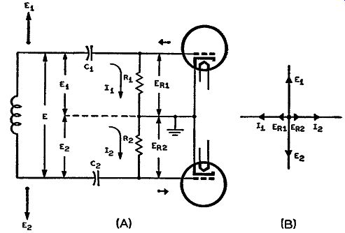
Fig. 4-6. The current and voltage distribution (A) In the input circuit
to the balanced modulator of Fig. 4-5 and the vector representation (B)
of these electrical conditions.
To clarify the relationship between the phase differences of the voltages across the secondary of the input transformer and those applied to the modulator grids, vectors are drawn close to the coil terminals and grids of the modulator tubes in Fig. 4-6 (A). We now come to the latter half of the dual-channel phase-shift balanced modulator circuit of Fig. 4-5, that part appearing after the load resistance R. Let us first analyze this circuit when no audio voltage is applied to the modulators. In this case no r-f output appears across the load resistance R. Connected to both ends of the secondary of the input transformer are two coupling resistors Ra and Rb. These resistors couple some of the r-f voltage appearing across the secondary directly to the grids of the first tripler tubes. This voltage is at the frequency of the crystal oscillator. To understand the phase relation ships between this coupled voltage and the sideband voltage as they both appear on the first tripler grids, we have to simplify the network appearing to the right of resistor R.
It is false to say that in Fig. 4-5 the capacitor C5 and the inductance Ls, or the capacitor C4 and inductance L4 constitute simple series tuned circuits. Although this may appear to be the case, the effect of the mutual inductance as caused by the coupling between L3 and L4 has to be taken into account. Inductance L5 and L4 are parts of a center tapped coil such that Ls and L 4 are wound in series aiding. This makes the mutual inductance additive to the total inductance across the complete coil. If the mutual inductance is designated as the letter M then the total inductance across the entire coil is equal to L3 + L4 + 2M.
However, if the inductance across each individual half of the coil is measured, the values found would be just L 3 and L 4 respectively.
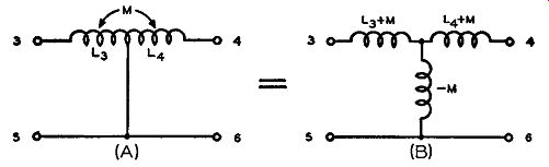
Fig. 4-7. The center-tapped coil, L3 and L,, of Fig. 4-5 is shown in
(A) with the indication that mutual inductance M exists between the two
halves of the coil. The equivalent network is shown in (B).
Due to these measurements the center tapped coil can be represented by an equivalent circuit. This circuit is shown in Fig. 4-7. In part (A) of this drawing the original coil is shown with the indication that mutual inductance exists between the individual halves and in part (B) the equivalent network is drawn. To show that they are equivalent we can measure the inductances between the respective terminals to see if they are the same. For example, across terminals 3 and 5 in Fig. 4-7 (A) we would measure L, and across the same terminals in Fig. 4-7 (B) we would measure (L8 + M) - M which is also equal to Ls because the M's cancel out. Similarly, across terminals 4 and 6 in part (A) we find L 4; across the same terminals in part (B) we have (L4 + M) - M which is also equal to L 4. Thus, it is seen that the two circuits are equivalent to each other.
With this in mind we can then simplify the other half of the net work of Fig. 4-5 not yet analyzed. This is illustrated in simplified form in Fig. 4-8. Capacitors C5 and C4 are both equal to each other, and so are the inductance values of L3 and L 4. The total inductance across points X and Y is L5 + L4 + 2M, and this total inductance is in resonance, at the crystal oscillator frequency, with the two series capacitors C8 and C4. Since at resonance a tuned circuit is purely resistive to the resonant frequency, the voltage from the secondary of the modulator transformer coupled into the tripler grid circuits through R0 and Rb does not change in phase. This means that the phase of the carrier voltage at the top of the modulator secondary is the same as that of the voltage at the upper tripler, and the phase of the carrier voltage at the bottom of the modulator secondary and at the lower tripler also are the same. These voltages at the tripler grids are smaller than those at the secondary of the modulator input transformer be cause of the voltage drop in coupling resistors Ra and Rb. Since Ra and Rb are equal to each other, the carrier voltages on the tripler grids are equal in magnitude. It should be remembered that, since the voltages at the secondary of the modulator transformer are in phase opposition (that is, 180° out of phase), so are the voltages at the tripler grids.
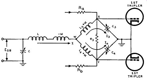
Fig. 4-8. Circuit equivalent to that coupling the double sideband output
of the balanced modulator to the grids of the tripler tubes of Fig. 4-5.
With audio applied to the modulator there appears a double side band output signal across the load resistance R of Fig. 4-5. Due to the 90° phase shift of the carrier input to the modulator, the double side band output is already 90° out of phase with the carrier signal across the secondary of the modulator transformer. This double sideband output appearing across the load resistor is designated as E8B in Fig. 4-8. The circuit that couples this sideband voltage to the tripler grids is shown in equivalent form in Fig. 4-8. Examining this equivalent circuit and the circuit of Fig. 4-5, it will be noted that capacitors C5 and C6 are omitted. The reason for this is that C5 is just a d-c blocking capacitor to prevent d.c. from getting on the tripler grids and C6 is just a bypass capacitor in the plate load circuit of the modulator tubes.
Both of these capacitors are high enough so that they have negligibly small reactances at the high frequency of operation and can be considered as r-f short circuits. The resistors and capacitors in the cathode circuits of the triplers are also omitted because, at the frequency of operation, the capacitors are likewise equivalent to a short circuit. So the cathodes are shown grounded as far as the r.f. is concerned.
We can also consider the resonant elements as the combination of two series resonant circuits. At resonance, the reactance of the series combination of C3 and C4 is equal to the reactance of the series combi nation of L5+ M and L 4
+ M. Since C3 equals C4 and L5+ M equals L4
+ M, the reactance of Cs alone equals the reactance of L3
+ M and the reactance of C4 equals the reactance of L4
+ M, both at the frequency of the crystal oscillator.
This means that Ls +M and Cs are in series resonance as well as L4 + M and C4
The resonance in each case occurs at the frequency where the reactances of the inductances and capacitances are equal, namely, the frequency of the crystal oscillator.
The resistance R3 is inserted to make the resonant circuits broad enough to have a selectivity that will admit the double sideband frequencies which, at peak proportions, may have a frequency 15 khz greater or less than the crystal oscillator frequency. This is so because the audio frequency is capable of going as high as 15 khz.
At resonance in a series tuned circuit the impedance is purely resistive and is at a minimum. This means that the L in Fig. 4-8 is in series with the mutual inductance -M ( effectively a negative inductance) and also in series with the low effective resistance offered by the two series resonant circuits to ground. Since capacitor C is connected between one side of the coil Land ground, it is in parallel with this series inductive and resistive arrangement. The value of L is so chosen that it is sufficiently greater than the "negative" inductance of -M to produce an effective inductance in parallel resonance with C at the crystal frequency. Therefore, the double sideband voltage E8n is delivered to a completely resistive load and undergoes no phase changes. Since the circuit is a parallel circuit, the same voltage E8n exists across each branch of the circuit. The reactance of the effective inductance ( of L and -M) is so much greater than the low resistance offered by the two series tuned circuits that that branch of the parallel circuit can be considered as almost a pure inductive circuit. As the voltage across an inductance leads the current through it by 90°, the current I flowing through the inductive branch of the parallel circuit is lagging the voltage E8n across it. This is shown by the two vectors Esn and I in Fig. 4-9 being 90° out of phase with each other, with voltage vector E8n leading. At the center tap of the coil, point Win Fig. 4-8, the current I divides equally into two parts, namely 18 and 14. The two circuits in which 13 and 14 appear, are at series resonance and purely resistive, and no phase change occurs in the two currents with respect to the original current I. This is shown vectorially in Fig. 4-9 where the two current vectors 13 and 14 are equal in magnitude and phase and coincide with each other; both of these currents in turn are equal to half of vector I and in phase with it. Since the currents 18 and 14 are equal and also since capacitors Cs and C4 are equal, the individual voltage drops across these capacitors are also equal. These voltage drops are designated as E08 and E04, respectively. Voltage across a capacitor lags the current flowing through it by 90°, and so voltage E03 lags current Is by 90° and voltage E04 lags current 14 by 90°. This is illustrated in Fig. 4-9. ...
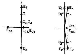
Fig. 4-9, left, 4-10 right. Vector diagram (left) of the electrical
quantities indicated in Fig. 4-8, where E1 and E2 arP. equal but opposite
phase crystal frequency voltages across C8 and C4 respectively. Fig.
4-10 is the vector diagram of the voltages appearing at the grids of
the triplers.
... where the two voltage vectors E08 and E04 are equal and in phase with each other, and where both are lagging the respective currents 18 and 14 by 90°. It should be remembered that voltages E08 and E04 are at the side band frequencies but of course reduced in amplitude. These voltages are considered the parts of the double sideband which are applied to the upper and lower tripler grids respectively. If the vector diagram of Fig. 4-9 is examined once more, it will be found that the two double sideband vectors E03 and E04 are 180° out of phase with the original double sideband signal E1 m appearing across the load resistance R.
The center frequency components of voltage coupled through resistors Ra and Rb from the secondary of the modulator input transformer are not changed in phase by the resistive effect of the resonant circuit, but are only reduced somewhat in amplitude. By having a ground between the two equal capacitors C3 and C4 and by having resistors Ra and Rb equal, equal but opposite phase crystal frequency voltages are applied across the individual capacitors. These voltages are designated as E1 (across C3 ) and E2 (across C4) similar to those crystal frequency voltages across the secondary of the modulator input transformer. These voltages, although 180° out of phase with each other, are each goo out of phase with the double sideband output voltage, EsB, from the modulator tubes. This is so because of the goo phase shift originally given the input crystal voltage to the modulator by the C1R1 and C2R2 phase shifting network. Since E1 and E2 are both 90° out of phase with EsB, their vectors are drawn as seen in Fig, 4-9. The vector diagram shows that voltages E1 and E03 which are across capacitor C3 and hence across the input to the upper first tripler tube, are 90° out of phase with each other. The same applies to vectors E, and E04 and capacitor C4 with respect to the lower tripler tube. Drawing another vector diagram with just the voltage vectors appearing across the input grid of the triplers and adding the respective voltages on each of these grids will give us a more vivid picture of the final voltage input to these tubes.
This is illustrated in Fig. 4-10, in which vectors Ex and Ey are the resultant voltages that occur after the double sideband voltage is combined with the crystal carrier signal. They are applied to the upper and lower tripler grids respectively. These two resultant signals are practically 180° out of phase with each other due to the small amount of sideband voltages as compared with carrier voltages. The modulator is operated so that, for less than one percent output distortion for 100 percent modulation (75- khz peak deviation), the peak phase deviation in either case (both being symmetrical) is 11.06 degrees for a 50-cycle audio input, which is equivalent to a 9.65-cycle peak frequency deviation.
Because of the symmetry of the complete system, the phase deviations of both resultant signal inputs to the tripler grids are equal.
Therefore, phase angles theta_1 and theta_2 in Fig. 4-10 are equal, but it is seen that Ex lags its center frequency component E1 by theta_1 degrees and Ey leads its center frequency component E2 by 02 degrees. Since vectors E1 and E, are 180° out of phase, the two resultant signals are approximately 180° out of phase, but when the frequency deviation of one is increasing (that is, phase leading), the frequency deviation of the other is decreasing (that is, phase lagging). When the audio signal progresses through 180° from the condition shown here, the vectors shown in Fig. 4-10 change their relative positions. Ecs and E04 shift 180°, with the result that Ex then leads Ei, and Ey lags E,. We thus see that the FM signal inputs to the two tripler grids are such that their center frequency components are equal to each other.
However, when the frequency deviation of one causes the resultant or instantaneous frequency to increase to a maximum, the frequency deviation of the other causes its resultant or instantaneous frequency to decrease to a minimum. This is the reason for the opposite polarity signs next to the deviation frequency in Fig. 4-4.
THE WESTERN ELECTRIC DIRECT FM TRANSMITTER
In contrast to the indirect FM system employed in Armstrong's transmitter, the transmitters of the Western Electric Company use direct FM by means of reactance tubes.
Besides the power stages there are two main sections of the direct FM transmitter. One section produces the actual FM signal, and the other section is the automatic frequency or stabilization control system. The production of an FM signal in the Western Electric transmitters is, as stated, one of direct FM, using balanced reactance modulators and a push-pull oscillator circuit. The important part of these transmitters is the method of stabilizing the center frequency of the push-pull master oscillator. This method of stabilization, or automatic frequency control, is quite different from that afc circuit discussed in Section 3. This system is a mechanical-electrical arrangement which uses a motor for correcting the center frequency of the oscillator. In conjunction with this type of frequency control a frequency dividing system is used which employs balanced ring modulators utilizing re generative feedback.
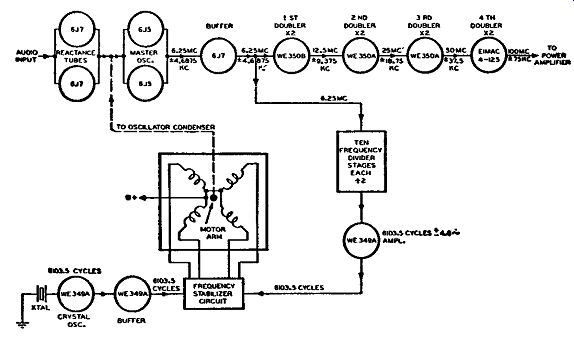
Fig. 4-11. Block diagram of the Western Electric FM transmitter without
the final power stages.
Before going into a separate discussion of these individual circuits lets us first study the block diagram of the Western Electric transmitters as operated today. In Fig. 4-11 we see such a block diagram, in which the power amplifier stages are omitted from the drawing.
This block diagram is representative of the transmitters that are operating on the new 88-to-108 -mhz band. The primary difference, so far as tube functions are concerned, between the new band circuit and the old band (42 to 50 mhz) transmitter arrangement, is that, in place of the last doubler tube shown in Fig. 4-11 an amplifier formerly was used. Thus, if Fig. 4-11 is examined it will be seen that four separate doubler stages are employed, and, hence, the total amount of frequency multiplication is equal to 16. For a peak frequency deviation of 75 khz (for 100 percent modulation) the peak frequency deviation at the output of the modulated oscillator or buffer stage is equal to 75/16 or 4.6875 khz. This contrasts with the transmitter operated on the old band, which employed only three doubler stages and, therefore, had a frequency multiplication of only 8. In this respect the peak frequency deviation at the output of the buffer (for 75- khz final output peak deviation) would have to be 75/8 or 9.375 khz - twice that employed in the new band transmitters.
In Fig. 4-11 the two separate sections, FM signal production and frequency stabilization, are readily noticed. If we assume that the transmitted center carrier frequency component is 100 mhz, the frequency of the master oscillator would be the division of 100 mhz by the amount of multiplication -which is 100/16 or 6.25 mhz. The value of the center frequency component of the FM signal, together with its peak frequency deviation, is indicated next to the input to the multi plier stages, denoting the frequency values of the FM wave as they enter the doublers.
The analysis of the direct FM system is straightforward, but that of the frequency control· system is quite different from any encountered as yet. This frequency stabilization system is briefly described as follows: Some of the output from the buffer stage is tapped off and applied to the input of a frequency divider system. This frequency divider system consists of ten frequency division stages with each stage having a frequency division equal to 1/2. That is, the input signal to one divider stage appears in the output of that stage at half its original frequency. Taking into account all the dividing stages, we have a total frequency division system wherein a division factor of 1/1024 exists.
This value of 1/1024 is obtained by multiplying 1/2 by itself 10 times.
The frequency input to the dividing system, as tapped off the output of the buffer stages, is equal to 6.25 mhz at a peak deviation frequency of 4.6875 khz. After passing through the complete system of frequency division, the output frequency will be the input frequency divided by 1024. Therefore, 6.25 mhz/1024 equals 6103.5 cycles and 4.6875 khz/1024 equals approximately 4.6 cycles.
From this analysis we find that the output signal from the dividing system is an FM signal that has a center carrier frequency component equal to 6103.5 cycles at a peak deviation of about 4.6 cycles. This amount of peak deviation for 100 percent modulation, may occur at the lowest audio frequency input, namely 30 cycles; and, at this deviation and audio frequency, the modulation index is about 0.15, which means that only two effective sidebands (one sideband pair) appear at the output of the dividing system. (See note at end of Table 1 in Section 2.) If the audio frequency is increased from 30 cycles, the modulation index will decrease, and the sidebands will never increase beyond one pair. However, as the audio frequency is increased and thus the modulation index decreased, the amplitude of the sideband pair decreases while that of the center frequency component increases.
As the number of dividing stages is increased, the frequency deviation decreases, which again means that the modulation index, for any one audio frequency, decreases. In turn this decreases the number of effective sideband pairs and also their amplitudes and increases the center carrier frequency component. In effect then, what a frequency dividing system does to an FM signal is to concentrate the energy of the FM signal into its center carrier frequency component. From what has just been discussed, it can be seen that the frequency deviation at the output of the dividing system, though it can never be greater than approximately 4.6 cycles, can be less. The lower the amount of this frequency deviation the better will be the operation of the stabilizing motor.
The output of the last dividing stage is injected into an amplifier using a WE349A pentode tube. The output from this amplifier is injected into a frequency stabilizing circuit. Also injected into this frequency stabilizing circuit is the output from a crystal buffer tube. The frequency of the crystal oscillator which is connected to the buffer tube is 6103.5 cycles, the same frequency obtained from the divider stages. The output of the frequency stabilizing circuit is injected into a four winding synchronous motor. When the output frequency of the master oscillator is exactly in tune, the frequency output from the divider stage is exactly the same as that of the crystal oscillator. In this respect the stabilizing circuit functions so that there is no phase difference in the magnetic fields set up between the different poles of the motor, and the shaft of the motor remains stationary. If the master oscillator becomes off tune due to some instability, the frequency output from the divider system will likewise change. This means that the input frequencies to the stabilizer from the divider system and crystal oscillator system are no longer the same. The frequency stabilizer system then produces a shift in the magnetic fields within the motor, and the magnetic fields rotate according to the difference in the two frequencies. The armature of the motor, being in the magnetic field, rotates according to this same difference in frequency. The armature shaft, being connected to the variable shaft of the master oscillator tuning capacitor, will change the capacitance of these capacitors so that the frequency output from the master oscillator will be stable again.
Balanced Modulator and Oscillator Circuit
Fig. 4-12. The modulator-oscillator stages of the Western Electric transmitter.
In the Western Electric transmitters the effect of direct FM by reactance injection is obtained in a somewhat different fashion from that discussed in the previous Sections. The circuit for the modulator oscillator stage is shown in Fig. 4-12. It essentially consists of a push pull oscillator circuit and a reactance tube modulator circuit employing two tubes wherein the plates are connected in push-pull and the grids in parallel so far as r.f. is concerned. The oscillator tank circuit consists of capacitors C1, C2, C3, C4, in parallel with inductance L1 and the injected reactance from the modulator tubes. Coil L2 is coupled to coil L1 and, by transformer action, some energy of oscillator frequency is induced into coil L2. This energy is passed through a goo phase-shifting network, shown in the dotted part of Fig. 4-12, and the output from this network is applied to the parallel grids of the modulator tubes. The modulator plates are connected across the oscillator tank circuit which in turn is connected to the oscillator plates. Since the input r-f voltage (of oscillator frequency) to the modulators is 90° out of phase with that voltage existing on the high side of L1, it is likewise 90° out of phase with the voltage existing on the high side of L1. The r-f plate currents of the modulator tubes are in phase with the voltages existing on the grids of the same tubes. The r-f plate currents of the modulators are therefore goo out of phase with the oscillator tank voltage.
To simplify all this, a simple vector diagram is drawn in Fig. 4-13.
In this diagram the voltage at the top of L1 is designated as E1. Then by transformer action the voltage Es at the high side of L5 is 180° out of phase with E1. This voltage E11 being subjected to a 90° phase shift is designated as voltage E11 as it appears on the modulator grids. (This phase shift causes a lagging 90° change.) It is the nature of amplifying vacuum tubes that the plate current is in phase with the voltage on the grid. The plate current of the modulators is designated as I in the vector diagram, and it is seen to be in phase with E11 , the phase shifted voltage on the grids of the modulators. Comparing the phase relationships of the vector diagram readily discloses that the r-f plate current I of the modulators is 90° leading the r-f oscillator voltage E1, at the top of L1. Although not shown in the vector diagram, I lags the voltage at the bottom of L1 by 90°, since L1 is connected in push pull.
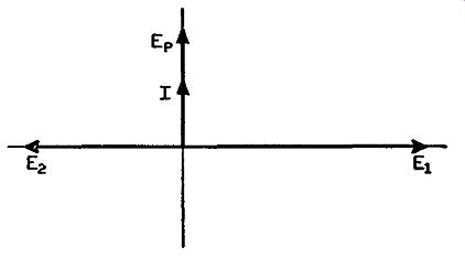
Fig. 4-13. Vector diagram of the voltages and current appearing in the
modulator circuit of Fig. 4-12.
Because the plate currents of the modulators are in quadrature with the voltages existing across L1 in their output circuit, the modulators effectively act as reactance tubes. This was brought out in Section 3, where reactance tube modulators were discussed, and also in Fig. 3-7.
In Fig. 4-13, the plate current I is leading the voltage E1 by 90°, so the injected reactance from the upper modulator tube would be capacitive. The modulator plate current, I, in the lower modulator tube lags the voltage across the lower half of L1 , and therefore, this modulator tube injects an inductive reactance. Without any audio voltage applied to the modulators constant values of injected reactance exist across the oscillator tuned circuit, which is part of the initial determining factor of the oscillator frequency. If an audio signal is applied to the modulators, the plate currents of both modulators change in accordance with the varying audio which is superimposed upon the bias to the modulator t1 .1bes, which is equivalent to changing the Ym of the tubes. Since the plate currents are quadrature currents, they are referred to as being reactive currents.
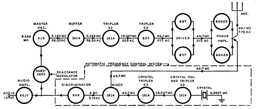
Fig. 4-14. Block diagram of the Columbia Broadcasting System FM transmitter
for the old FM band. The center frequency was 46.7 mhz.
The audio signal is applied to the modulator tubes in push-pull, so that the audio voltages on their grids are always of opposite polarity.
When on one-half of the audio signal the bias on the upper tube is decreased by a certain amount, the bias on the lower tube is increased by the same amount. Or, the Ym of the upper tube is increased while that in the lower tube decreases. The capacitance injected by the upper tube will increase, because it is directly proportional to g.,. of the upper tube. The inductance injected by the lower tube will also increase because it is inversely proportional to the gm of the lower tube, and the gm is decreasing. Consequently, an increasing capacitance and inductance is injected across the oscillator tank circuit at the same time. Both reactive components cause the frequency of the oscillator to decrease.
When the audio signal is such that the bias on the upper tube de creases, the bias on the lower tube increases. Consequently, the g,,. of the upper tube decreases, while in the lower tube it increases. Due to this action the injected capacitance from the upper tube and the injected inductance from the lower tube both decrease, causing an increase in the frequency of the oscillator. Under the same conditions of audio input, the frequency swing that the oscillator is subjected to is greater than if only one reactance tube were used, for the reason that both tubes inject reactances which cause the oscillator to shift in frequency in the same direction. The amplitude of the audio signal determines the amount of oscillator frequency swing (that is, deviation), and the frequency of the audio signal determines the rate of change of the frequency deviation, and thus an FM signal output is obtained.
From the high side of L2 some FM voltage is injected into the grid of the buffer stage which in turn is connected to the frequency multiplication and division systems. The capacitors of the tank circuit are so arranged that C8 and C4 are ganged and are varied together by manual means. Capacitors C1 and C2 are also ganged, but the shaft of this ganged control is attached to the shaft of the synchronous control motor and thus capacitors C1 and C2 are automatically variable to correct for frequency drift of the master oscillator.
THE CBS DIRECT FM TRANSMITTER
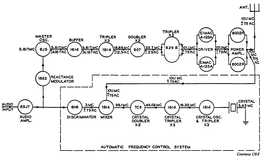
Fig. 4-15. Block diagram of the CBS FM transmitter for the new FM band.
The new center frequency is 101.1 mhz.
The new FCC frequency allocations giving the 88-to-108 -mhz band to frequency modulation were released in the fall of 1945. This was just after World War II ended, and many companies had war con tracts to terminate, which prevented the immediate production of new FM transmitters. The Columbia Broadcasting System (CBS), in order to remain on the air on the new band, decided to convert the old-band FM transmitter to the new band as soon as possible. The conversion idea was adopted because of limitations in time and material at that time. A block diagram of the circuit for the old band is shown in Fig. 4-14 and for the new band in Fig. 4-15. Both employ reactance tubes for direct FM and also automatic frequency control systems of the electronic kind described in Section 3. The center frequency of trans mission on the old band was 46.7 mhz and on the new bandit is 101.1 mhz.
Referring to Fig. 4-14, the transmitter setup as operated on the old FM band, a frequency multiplication of 9 is provided by the use of two triplers. Thus the master oscillator center frequency is equal to 46.7 mhz/9 or 5.189 mhz. At the output of the last tripler, an 807 tube, the FM output is at its required frequency and is impressed across a push-pull driver stage consisting of two 807's. This push-pull stage is the driver for the final power amplifier stage which is also a push-pull stage and consists of two 8002R's. The peak frequency deviation is shown, with plus and minus signs, as well as the center frequency component of the FM signal, at the respective input sections to the different stages of the set.
For the automatic frequency control system employed, the output intermediate frequency from the mixer is 3 mhz. Some of the 46.7-mhz FM output signal from the final power amplifier stage is injected in this mixer. Also injected into the mixer is a 43.7 -mhz unmodulated signal from a crystal oscillator system. This crystal oscillator system consists of a 4.8557 -mhz crystal oscillator and two triplers, so that the final output from this system is 4.8557 X 9 or 43. 7 mhz. The function of first tripler and crystal oscillator is accomplished by the same 1614 tube. From the two inputs to the mixer it is readily seen that the difference frequency between 46. 7 mhz and 43.7 mhz is 3 mhz. The rest of the afc circuit is of conventional design, where the output of the discriminator is applied to the grid of the reactance tube, thereby opposing any shift of the center frequency of the master oscillator.
In Fig. 4-15 the new FM circuit is drawn in block diagram form.
An extra multiplication stage, an 807 doubler, and an extra crystal multiplier, a 7C5 doubler, are the primary changes in the circuit design. Since the frequency of transmission is changed, the master oscillator and crystal oscillator frequency are likewise changed. The multiplication stages employed are a tripler, doubler, and tripler in the order named. Thus, the total amount of multiplication is 3 X 2 X 3, or 18. With the frequency of transmission 101.1 mhz, the master oscillator frequency will have to be 101.1 mhz/18 or 5.617 mhz. Similarly, for a 75- khz peak deviation output for 100 percent modulation the initial peak deviation of the FM signal from the modulated oscillator is 75/18 or 4.167 khz. Thus, we obtain an FM signal of a center frequency of 5.617 mhz with an initial peak frequency deviation of 4.167 khz that is impressed across the first frequency multiplier stage, namely a tripler. The last multiplication stage, also a tripler, is a push-pull stage using an 829-B duo-beam power tube. This 829-B multiplier, besides being used as a tripler, is also a driver for the push-pull power driver which utilizes two Eimac 4-125A's.
Only two changes were made in the automatic frequency control system used on the old band. The crystal was changed from 4.8557 mhz to 5.45 mhz and a doubler tube was inserted between the last tripler and mixer stage. This arrangement made it possible for a higher un modulated crystal controlled frequency to be injected into the mixer tube. The crystal multiplication setup has the same amount of multiplication as the FM section. That is 3 X 3 X 2 (tripler, tripler, and doubler) gives a total multiplication of 18. This means that the crystal controlled frequency input to the mixer tube is equal to 5.45 mhz X 18, or 98.1 mhz. This unmodulated 98.1 -mhz signal plus the FM 101.1 -mhz signal taken from the output of the final power amplifiers are both injected into the mixer. The output circuit of the mixer is tuned to the difference frequency between these two signals, so that an i-f signal of 3 mhz is injected into the discriminator stage. The rest of the action of the control circuit is familiar enough not to warrant any further discussion.
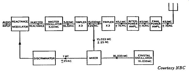
Fig. 4-16. Block diagram of the old band NBC direct FM transmitter operating
on a center frequency of 45.1 mhz.
Fig. 4-17. Block diagram of the NBC FM transmitter operating at 97.1
mhz. This differs from the transmitter of Fig. 4-16 primarily by the
addition of an extra multiplication stage and a change in the stabilization
circuit.
THE NBC DIRECT FM TRANSMITTER
Before the FM band of 88 to 108 mhz was allocated, the FM transmitter of the National Broadcasting Company in New York City was transmitting an FM signal of 45.1 mhz. The block diagram for this transmitter is illustrated in Fig. 4-16. It will be noticed that the type of frequency control is an automatic frequency control system (afc) similar to that discussed in Section 3. The type of modulation is direct FM, wherein the modulators inject some reactance into the tuned oscillator circuit. For the center frequency output of 45.1 mhz, the master oscillator frequency is tuned to 5.011 mhz, due to the use of two tripler multipliers. What we have is 5.011 mhz multiplied three times, and the output of the first tripler is equal to 5.011 X 3 or 15.033 mhz.
This is injected into another tripler which changes the frequency to 15.033 X 3 or 45.1 mhz. The 45.1 -mhz output is then passed through the proper power amplifiers for transmission. The initial amount of peak frequency deviation of the FM signal, as it enters the first tripler, must be equal to 8.33 khz in order that its output, when multiplied 9 times by the two triplers, be equal to 75 khz for 100 percent modulation.
From the output of the first tripler some of the FM signal of 15.033 -mhz center frequency component is injected into a mixer stage.
Also, into this mixer stage is injected a crystal controlled oscillator frequency of 16.033 mhz. In the output circuit of the mixer is a tuned circuit that selects the 1 -mhz difference frequency between the two input signals. This 1-mhz signal is applied to a discriminator tube, and the output from this discriminator is impressed across the grids of the modulator tubes. If the oscillator becomes unstable, this afc circuit functions so that the injected reactance across the oscillator circuit changes in the direction necessary to put the oscillator back on frequency.
For the FM band of 88 to 108 mhz, station WNBC received the frequency allocation of 97.1 mhz. Today station WNBC operates only on this new frequency assignment, having discarded the old transmitter setup. Instead of revamping the old circuit they incorporated a new transmitter, the block diagram of which is illustrated in Fig. 4-17. In this transmitter two primary changes have been made, one being the addition of an extra multiplication stage and the other the changing of the frequency control or stabilization circuit.
This is noticed in Fig. 4-17. In analyzing this diagram let us first start with the FM section. The type of modulation is direct FM, similar to that used on the old band. That is, reactance tubes frequency modulate the oscillator, and the output is a direct FM signal which is injected into the multiplication system. Two frequency triplers and one doubler are employed to give a total frequency multiplication of 18 (that is, 3 X 3 X 2). Therefore, since the output frequency is 97.1 mhz, the frequency of the master oscillator must be 97.1 mhz/18 or 5.394 mhz. Likewise, for a 75- khz peak deviation output for 100 percent modulation, the peak deviation of FM signal as taken from the oscillator-modulator stage is equal to 75 khz/18 or 4.167 khz. This FM signal of 5.394-mhz center frequency component in conjunction with a peak deviation frequency of 4.167 khz is injected into two tripler stages.
The respective frequency multiplication is indicated by the values of the center frequency component and peak deviation frequency on the diagram. The output of the second tripler being at 48.55 mhz is impressed across a driver amplifier, and the output of this amplifier, still at 48.55 mhz, is impressed across another multiplication stage, namely a doubler. This doubler brings the FM signal to its required value of 97.1 mhz and the signal is then injected into the power stages of the transmitter.
Frequency Stabilization System (RCA)
The frequency stabilization system of this transmitter is motor controlled similar to the system employed by Western Electric. The frequency stabilization system is a design of the Radio Corporation of America (RCA) and is incorporated in the type BTF FM broadcast transmitters as manufactured by RCA. This frequency control system is shown in block diagram form below the FM section of NBC's transmitter of Fig. 4-17. It consists chiefly of three sections: One called the frequency division section, another called the crystal oscillator section, and the third called the motor control section.
Part of the output FM signal from the master oscillator section is fed through a series of frequency divider stages. The division of each stage is plainly marked inside the block diagram for each stage, and the total amount of division is therefore 3 X 4 X 4 X 5 or 240. This means that the input FM signal from the modulated oscillator to the first divider being 5.394 mhz (and 4.167- khz peak deviation) undergoes a division of 240. Therefore, the output frequency from the last divider stage is 5.394 mhz/240 or 22.476 khz and 4.167 khz/240 or 17.363 cycles is the peak deviation. The output from the crystal oscillator of 112.38 khz is put through a divider stage of 5, so that the output from the divider stage is equal to 112.38/5 or 22.476 khz, the same frequency as that from the FM divider stages. If the master oscillator is stable, its frequency will be 5.394 mhz and the output from the FM dividers 22.476 khz. The output from the crystal divider is split up and is sent through two separate 45° phase-shifting networks so that the phase relationship between the output signals of the two phase shifters is 90°. Both of these signal outputs are fed into separate balanced modulator circuits.
Also fed into these balanced modulator circuits is the output signal from the FM frequency divider system.
The outputs of both these balanced modulators are fed into a four winding 2-phase motor. If the frequency outputs of both divider systems are the same, the magnetic fields of the motor are steady. however, if the master oscillator becomes unstable and the output frequency shifts from its center component of 5.394 mhz, the output from the FM divider stage changes from its 22.476- khz signal, and a different frequency is impressed across the balanced modulators. These balanced modulators function so that a difference of frequency between their two input signals causes the outputs of the modulators to change the magnetic fields of the motor and the armature of the motor rotates.
The shaft of the armature is connected to the rotor shaft of a split stator capacitor in the master oscillator tank circuit. The armature rotates, due to un-stability of the master oscillator, turning the oscillator capacitor to the extent that it changes the frequency of the master oscillator back to its stable position. In other words, if the master oscillator shifts in frequency by an increase of 50 khz, the frequency output of the divider system will be:
5394 + 50 = 5444 _ 22 685 k 240 240 - . C
This means a difference in frequency between the two inputs to the balanced modulators of 22.685 less 22.476, or 207 cycles. The outputs of the balanced modulators will change the magnetic field of the motor in accordance with the 207-cycle difference and the armature will rotate. The rotation of the armature, according to this 207-cycle difference of the inputs to the balanced modulators, is such that the split stator capacitor is varied just enough to change the frequency of the master oscillator by 50 khz back to its desired value.
THE GENERAL ELECTRIC TRANSMITTER
The original FM transmitters manufactured by the General Electric Company were the direct FM type employing the regular electronic automatic frequency control system similar to that discussed in connection with the CBS transmitter. The FM multiplication system in these original transmitters employed two triplers for a total frequency multiplication of 9. In the new FM transmitters the General Electric Company employs a completely different system. The new system is one of indirect FM where p.m. is the initial type of modulation. By using the proper audio frequency correction network the p-m signal is made equivalent to an FM signal. The method of obtaining the initial amount of phase deviation is new. In these transmitters the famous Phasitron tube is employed as the modulator and the operation of the transmitter is based upon this tube. Before we analyze the complete exciter and modulator system, let us first study the Phasitron tube and see how it works.
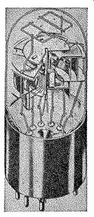
Fig. 4-18, right. Cutaway view of the Phasitron tube, which is used
as the modulator and upon which the operation of the GE FM transmitter
is based.
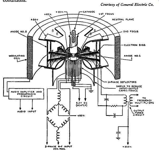
Fig. 4-19, below. Sketch of the functioning elements of the Phasitron
tube and a simplified schematic diagram of the circuits to which they
are connected. Above and below the electron disk is the deflection system.
The deflector grids consist of 36 wires every third one being connected,
making three grids each having 12 wires.
The voltages indicated in this and the next figure are typical of slightly different operating conditions.
The GE Phasitron Tube
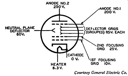
Fig. 4-20. Schematic symbol of the Phasitron tube with typical operating
voltages indicated at the various elements.
The Phasitron tube enables us to obtain wide phase deviations, equivalent to a peak frequency deviation of about 175 cycles, from a crystal controlled source of about 200 khz. The tube itself is quite a complicated structure so far as regular electron tubes are concerned.
It more nearly belongs to the class of the cathode-ray tube than to any other type, although its size is comparatively small. A cutaway pictorial view of the Phasitron tube is shown in Fig. 4-18, while Fig. 4-19 provides a more technical cutaway view of the functioning elements together with a simplified diagram of the circuit elements to which it is wired. In Fig. 4-19 all the parts shown are definite physical parts, except the so-called electron disk which is formed by a constant stream of electrons emanating from the cathode and focused on anode No. 1. A schematic diagram of the Phasitron tube is shown in Fig 4-20 with typical operating voltages shown alongside each electrode.
The heater voltage is at 6.3 volts. When typical operating voltages (such as those indicated in Figs. 4-19 or 4-20) are applied to the tube, electrons begin to flow away from the cathode toward the two anodes. Without any external r-f voltage applied to the tube, the focusing electrodes regulate the electrons flowing away from the cathode so that they flow in a radial fashion and are concentrated into a thin electron disk, the shape of a flat plate. Above and below this disk is a deflection system. Above the electron disk is the so called neutral plane of the deflector system, and below the disk are the deflector grids. There are 36 deflector wires, so arranged that every third wire is connected together, making 3 grids with 12 connected wires in each. All the deflector grids and the neutral grid have d-c potentials applied. The deflector grids are, however, excited by an additional r-f voltage while the neutral grid is not. Therefore the neutral deflector (referred to as the neutral plane} remains as a source of reference potential for the other deflector grids. The r-f voltage is a 3-phase voltage obtained from a crystal controlled source.
This crystal voltage passes through a phase-splitting network making the r-f voltages applied to each deflector grid group 120° out of phase with each other. For correct operating procedure, the amount of r-f voltage should be approximately 35 volts rms as measured between each deflector grid and the neutral plane deflector. These 3-phase voltages as applied to the deflector grids deflect the electron disk so that the outer edge of the disk takes on a sinusoidal shape as seen in Fig. 4-21. In other words, there now exists an electrostatic field between the neutral deflector plane and the deflector grids, due to the application of these 3-phase voltages. This electrostatic field, due to the deflecting action of the deflector grids, distorts the flat electron disk into the shape shown in Fig. 4-21. The electrostatic field also produces an effect as though the sinusoidal electron disk were rotating at a rate determined by the frequency of the applied 3-phase voltage and the number of deflector wires.
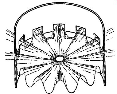
Fig. 4-21, left. A portion of the Phasitron perforated No. 1 anode through
which the sinusoidally distorted electron disk flows; under this condition
No. 2 anode receives a maximum current.
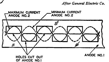
Fig. 4-22, right. The solid sine wave indicates the condition shown
in Fig. 4-21. The dotted wave shows the electron disk one-half an r-f
cycle later when a minimum current flows in the No. 2 anode.
The elements of the Phasitron tube are so arranged that this sinusoidally edged electron disk falls upon the specially constructed anodes of the tube. Both anodes are cylindrical, but anode No. 1 is of special construction. This anode has 24 holes punched into it, so arranged that 12 of these holes appear above and 12 below a certain dividing line. The dividing line is at the level of the electron disk before it is sinusoidally distorted by the application of the 3-phase r-f voltages.
Part of this anode appears in Fig. 4-21 in conjunction with the sinusoidally distorted electron disk. A flattened portion of this first anode is also shown in Fig. 4-22. The punched holes are arranged to be in line with the sinusoidal rim of the electron disk. Anode No. 1 is nearer the cathode and anode No. 2, which is a cylindrical electrode without any holes punched in it, lies directly behind anode No. 1, as illustrated in Fig. 4-19.
When r-f 3-phase voltages are applied to the deflector grids, the electron disk will become distorted, and the edge of the disk will take on a sinusoidal shape. Let us now refer to Fig. 4-22. This diagram shows by the solid line sine wave a picture of part of anode No. 1 at the instant when the rotating disk is aligned to anode No. 1 so that the upper halves of the sine wave part of the disk are passing through the top 12 holes of the anode, and the lower halves of the sine wave pass through the bottom l2 holes of the anode. Under this circum stance these electrons forming the electron disk are practically all passing through the holes of the first anode and, therefore, hitting the second anode directly in back of it. Consequently, at such an instant there is maximum current flow to anode No. 2 and a minimum current flow to anode No. 1. If the electron disk is rotated by just one-half cycle of the sine wave, the situation will be completely reversed. This is also shown in Fig. 4-22, where the dotted sine wave represents the edge of the electron disk one-half cycle of r.f. later. It is readily seen that the electrons forming the disk no longer pass through the holes in anode No. 1 but that most of them impinge upon anode No. 1 and a very few reach anode No. 2. Under this circumstance, the current flowing to anode No. 1 is a maximum and that flowing to anode No. 2 is a minimum.
Fig. 4-23. Pictorial representation of the Phasitron electron disk while
being phase shifted by the magnetic field set up by the modulating coil.
For the time between these two instances the current in one anode is decreasing while that in the other is increasing, and after they have reached their maximum decrease and increase, the situation reverses itself. The current that was decreasing in one anode now starts to increase and that which was increasing now starts to decrease.
Connected to the anodes of the Phasitron is a push-pull tuned circuit as shown in Fig. 4-19. The circuit is tuned to the crystal frequency and, since each end of the circuit is connected to an anode, this circuit is excited by the periodic collection of electrons by both anodes. Thus it is seen that the output push-pull circuit connected to the anodes is driven at the crystal frequency but, due to the currents in the anodes, the excitation is in a special time and phase relationship. Inductively coupled to this push-pull circuit is a single tuned circuit which serves as the input circuit for the first multiplier tube, and hence the multi pliers get their excitation from this coupling arrangement.
Now we come to the important part wherein the phase modulation is produced by an audio signal. Wrapped around the outside of the glass envelope of the Phasitron is the modulator coil which is solenoid wound. Part of this coil is seen in cutaway view (without the glass envelope of the Phasitron tube shown) in Fig. 4-19. This modulator coil, by means of electromagnetic deflection, phase modulates the electron disk. With the proper input audio signal applied to the modulator coil, a magnetic field is set up by this coil, and the coil is so arranged that the magnetic field is perpendicular to the plane of the electron disk. Due to this magnetic field, the electrons encounter a force such that the sinusoidal ripples of the disk experience a phase shift in direct accordance with the audio modulating signal. In other words, the modulating signal, since it varies at an audio rate, shifts the phase of the sine wave edge of the electron disk in an increasing and decreasing motion according to positive and negative portions of the audio signal. The magnetic field created by the coil is concentrated, because of the magnetic material of which the second focusing electrode is made, to a narrow portion of the tube at the rim of the deflector grids; proper phase shift action upon the electron disk is then produced within the punched hole regions of the first anode, as seen in Fig. 4-23. Thus, this second focusing electrode serves two purposes -- electrostatic focusing of the electron disk and electromagnetic focusing of the audio magnetic field.
Since the electron disk is now being changed in phase, according to the audio magnetic field, the output signal of oscillator frequency from the Phasitron, which is coupled to the multipliers, is also changed in phase according to the audio signal. Thus, we have a system of directly phase modulating a high frequency signal. In order to have the output signal from the Phasitron effectively frequency modulated, the impedance of the modulating coil is practically a pure reactance over the complete range of audio frequencies of 50 to 15,000 cycles.
As the audio frequency increases, the reactance also increases, in which case the. current flowing through the coil decreases. Therefore, as the audio frequency increases, the magnetic field decreases, due to the decrease in current, thus giving the desired inverse frequency effect. This is similar to the effect of the audio frequency correction network in the Armstrong transmitter, wherein an inverse audio frequency network was needed effectively to produce FM from p.m.
Consequently, with all of these provisions, the modulation of the Phasitron tube by the audio signal has the effect of speeding up and slowing down the rotation of the electron disk along its edge ( as shown in Fig. 4-23) which results in an FM output signal. The importance of this Phasitron tube is that it can produce wide phase shifts in the crystal frequency and, with the proper modulation arrangement, these phase shifts are equivalent to an FM signal that has peak deviations as high as 175 hz. Due to this wide deviation only a small amount of multiplication is needed as compared with other in direct FM systems. The amount of phase shift required for this 175 hz peak frequency deviation does not go beyond the allowable amount of harmonic distortion. The audio frequency harmonic distortion for all frequencies from 50 to 15,000 cycles is less than 1.5 percent rms.
Exciter and Multiplier Units
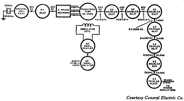
Fig. 4-24. Block diagram of the General Electric FM transmitter; the
power amplifiers are omitted.
A block diagram of the exciter unit of the GE transmitter is shown in Fig. 4-24. This part of the system comprises the a-f, r-f, and modulator units. It essentially consists of a crystal oscillator and an r-f amplifier feeding into the 3-phase network input to the Phasitron tube. Also the audio input is passed through two a-f amplifiers before it is impressed across the modulator coil. The output of the Phasitron tube, being an FM signal, is fed to a series of seven multipliers having a total multiplication equal to 432. The first three multipliers are doublers using 6SJ7 receiving type tubes, and hence a multiplication of 2 X 2 X 2 or 8 is obtained. The next two multipliers are triplers, also employing 6SJ7 tubes, and their multiplication is 3 X 3 or 9; from the input to the first 6SJ7 doubler to the output of the last 6SJ7 tripler the total multiplication is 8 X 9 or 72. The last two multipliers are a doubler and a tripler, respectively, making a multiplication of 2 X 3 or 6 and a total over-all multiplication of 72 X 6 or 432. The last multiplier (a tripler) employs a GL815 tube which, besides being a multiplier, is also the driver for the power amplifier stage succeeding it. The next to the last multiplier, a doubler, uses a 6V6 tube to supply the small amount of power needed to drive the GL815 tripler tube.
For 100 percent modulation, the output FM signal must have a peak deviation of 75 khz. This means the necessary amount of FM that occurs within the Phasitron tube has to be exactly equal to the maximum allowable peak frequency deviation divided by the total amount of multiplication. Thus 75 khz/432 equals 173.6 cycles, which means that the output peak frequency deviation from the Phasitron tube is equal to 173.6 cycles. The individual multiplication of this frequency deviation is illustrated in plus and minus signs next to the particular stages.
If an output FM signal of 97.2-mhz carrier frequency is desired to be transmitted, the frequency of the crystal oscillator would have to be equal to 97.2 mhz/432 or exactly 225 khz. This is indicated in Fig. 4-24 along with the respective increase in frequency as the signal is passed through the different multiplication stages. Since the new FM band is between 88 and 108 mhz, the crystal frequency has to be between 88 mhz/432, or 203.7 khz, and 108 mhz/432, or 250 khz.
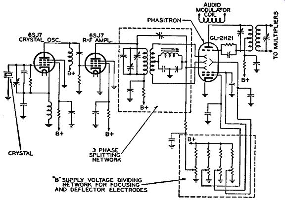
Fig. 4-25. Crystal oscillator and Phasitron circuits of the General
Electric FM transmitter.
A schematic diagram of the crystal oscillator and Phasitron circuit is shown in Fig. 4-25. The crystal oscillator is of the Colpitts electron coupled type wherein the cathode, control grid, and screen grid act as the crystal oscillator section of the 6SJ7 tube. In this instance, the screen grid serves as the oscillator anode, and the electron coupling occurs between this anode and the plate of the 6SJ7 tube. The output of the second 6SJ7, an r-f amplifier, is tuned-transformer coupled to a 3-phase-splitting network shown enclosed in the dotted box. The output from this phase-splitting network is applied to the three deflector grids of the Phasitron tube. The deflector grids, neutral plane deflector, and focusing electrodes all receive their B supply through a special voltage divider network consisting of four fixed resistors and four potentiometers. These potentiometers are preset so that the correct amount of B supply voltage is applied. to these Phasitron electrodes for the proper operation of the tube.
THE FEDERAL DIRECT FM TRANSMITTER
The Federal Telephone and Radio Corporation employs direct FM by means of injecting reactance into the oscillator tuned circuit. The interesting thing here is that the method of reactance injection is different from what we have studied thus far. Another interesting thing about these transmitters is the crystal automatic frequency control system which is used to stabilize the center frequency of the master oscillator. The modulator-oscillator unit in conjunction with the frequency control system is trade-marked by Federal as their Frequematic FM modulator system. In the analysis to follow we will discuss three phases of these transmitters. First, the oscillator-modulator unit will be studied, second the frequency multiplier system is discussed, and finally the frequency control system is analyzed.
The Oscillator-Modulator Unit
A simplified schematic diagram of the oscillator and modulator is shown in Fig. 4-26. The oscillator circuit is a conventional Hartley oscillator where the high side of the tuned circuit is connected to the grid of the tube and the cathode is tapped to the inductance of the coil. The modulator tube is a pentode having a tuned circuit in the plate load. Through the use of the "Miller effect" this modulator tube is made to inject a capacitance across the oscillator tank circuit.
An amplifier tube possesses a certain effective grid input impedance which is measured between grid and ground. The value of this grid input impedance changes in accordance with the plate load of the tube.
This type of effect is commonly known as the Miller effect. If the plate load impedance of the tube has both a resistive and reactive component at a specific frequency, the grid input impedance also contains both a reactive and a resistive component. However, if the plate load impedance is purely resistive, the grid input impedance is purely capacitive.
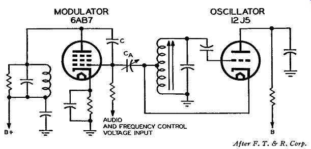
Fig. 4-26. Simplified schematic of the modulator and oscillator circuits
of the Federal FM transmitter.
In the modulator in Fig. 4-26 the plate load is a tuned circuit, so that at its resonant frequency it will offer a pure resistive load. As a result the grid input impedance of the 6AB7 tube will be purely capacitive, and a pure capacitance is injected across part of the oscillator tank circuit, thereby changing its resonant frequency. The whole crux of the situation is knowing what determines the value of the grid input impedance; and in this circuit with the resistive plate load, we know that the impedance is capacitive. Though it is beyond the scope of this guide to delve into the derivation of the following equation, it can be shown that the grid input capacitance for an amplifying vacuum tube that has a resistive load is as follows:
C1= Cgk + (1 + A) Cgp
…. where Cgk = the interelectrode grid to cathode capacitance, Cgp = the interelectrode grid to plate capacitance, A = the gain of the tube, and C1 = the grid input capacitance.
If the tube is a pentode, the gain A can be shown to be equal to the product gmRr, where gm is the transconductance of the tube and RL the effective plate load resistance. Consequently, we can replace A by g.,,RL in the above formula and the result will be:
Ci= Cg1,; + (1 + gmRL) Cgp
In Fig. 4-26 an extra capacitance C is inserted between the grid and plate of the tube, so that it will effectively add to the grid to plate interelectrode capacitance C{IP· The grid input capacitance C1 then becomes: Ci= Cgk + (1 + g.,.RL) (Cgp + C)
The value of the Cgp for the 6AB7 tube is equal to 0.015 µ.µ.f, and the value of C used in this transmitter is much higher than Cgp (being 5 µ.µ.f). Consequently, in the foregoing equation the value of c_gp,, can be neglected for computation purposes, because its effect will be negligible. Besides the actual value of the grid-to-cathode interelectrode capacitance C11k, stray wiring capacitance also must be taken into account, so that we may consider the over-all effective grid-to cathode capacitance of the 6AB7 tube to be equal to about 15 µ.µ.f. This takes into account the 8 µ.µ.f "input capacitance" of the 6AB7 tube itself. Under these circumstances, the final equation for the input capacitance is the following:
C, = 15 + (1 + gmRL)5 (neglecting C11,,) C, = 15 + 5 + 5 gmRL C, = 20 + 5 g,,.RL or 20 + 5A
This last equation tells us that the value of the input grid capacitance is equal to a constant, namely 20 µ.µ.f plus a variable component which depends upon the Ym of the tube. This variable component is equal to the capacitor C (5 µ.µ.f) multiplied by the load resistance and gm of the tube. If the value of RL is kept constant along with C, Ym is the only variable, and the value of c, can be made to change in accordance with the g,,. of the tube.
If no audio signal is applied to the modulator grid, a fixed value of Ym exists, and thus a fixed value of C, exists. The Ym of the tube, under these static conditions, depends upon the supply voltages and the bias on the tube, which consists of the fixed cathode bias plus the control circuit voltage impressed onto the grid. For there to be a resistive load in the modulator plate circuit, the tuned circuit must be resonant to the frequency of the master oscillator. If this plate circuit is detuned in any manner whatsoever by drift, or by changing of the oscillator frequency due to the modulation effect, there will be a resistive component in addition to the capacitive component in the grid input impedance of the tube. This is undesirable, because the resistive component in the grid input impedance will also be reflected across the oscillator tank circuit thereby introducing a-m effects. In order that no appreciable detuning occur, the tuned plate circuit of the modulator tube is made very broad (that is, the plate tank circuit is given a low Q) by paralleling a resistor across it. This is evident in Fig. 4-26.
Under these circumstances of a low Q tank circuit in the plate of the modulator tube and no audio applied to the modulator tube, a specific fixed value of grid input capacitance is injected across the oscillator tank circuit between the tap on the oscillator tank coil and ground. Therefore, the frequency of operation of the oscillator with no signal applied is dependent upon the inductance and capacitance of the oscillator tank circuit plus the value of the injected capacitance between the tap on the oscillator tank coil and ground.
With an audio signal applied, the g,,. of the tube changes (as discussed under the topic of reactance tubes in Section 3), and the last equation encountered reveals that the value of the grid input capacitance also changes, thereby varying the resonant frequency of the oscillator tuned circuit. Because the gm changes with change in audio amplitude, the frequency of the oscillator likewise changes in accordance with the changing audio amplitude. The result is that the oscillator signal becomes frequency modulated with a peak frequency deviation proportional to the amplitude of the audio modulating signal and a rate of change equal to the frequency of the audio modulating signal.
A series of measurements were taken on this modulator stage with various values of bias between the grid and ground of the modulator tube, and the gain of the stage was computed. The method was very simple. An r-f vacuum tube voltmeter was placed between grid and ground and another between the plate and ground of the tube, and the ratio of these two vacuum tube voltmeter readings, as a function of the grid voltage Ee, was determined to be the gain A. In Table 3 for different values of Ee, the gain A and the computed values of c, are tabulated.
TABLE 3

Adjustable coupling capacitor CA in the circuit of Fig. 4-26 is inserted to couple the modulator grid circuit to the oscillator tank. This capacitor is made adjustable, so that for a certain change in grid voltage, a fixed frequency swing (that is, frequency deviation) is obtain able at any particular oscillator frequency. If this capacitance CA were connected to the high side of the oscillator tank coil, a great deal of r-f signal from the oscillator would appear on the modulator grid. This is not wanted, so the capacitance CA is tapped to the oscillator coil, reducing this value of injected r-f signal, and, hence, the injected grid input capacitance appears across only part of the oscillator tank coil.
The actual capacitance that is injected across the cathode tap of the 12J5 oscillator tank coil is determined by the input capacitance C, of the modulator tube in series with the variable capacitor CA. Since these two capacitances are in series their total capacitance, call it CR, is as follows:
C _ CA X C, R- cA+c.
As used in this experimental run, the value of CA was measured on a Q meter and found to be equal to 55 µ.µ.f. Consequently, from the different values of Ci in conjunction with CA, a series of values of C.4. X c., C,1 + C,, and hence C1i were computed as shown in Table 3.
The value of CR is not the actual capacitance injected across the complete oscillator tank circuit but only across the tapped cathode part of the tank. To determine the effective value of injected capacitance across the entire oscillator tank a so-called transfer ratio between the tapped portion and the whole coil was found. The transfer ratio is equal to some constant value, designated as the letter K, and from this known value of K the final total effective capacitance, CT, across the entire oscillator tank is equal to:
CT= KC R
.... where CR is as explained before. From experiment K was found to equal 0.23, and therefore CT was equal to 0.23 C_R.
Next to the column of CR in Table 3 are the computed values of CT, using K equal to 0.23.
The next column gives the change in effective injected capacitance, CD, from the reference value of CT when Ee is zero. When E0 is zero, C7, is 6.75; therefore, CD=CT-6.75 For example, for 5 volts Ee the change in capacitance CD is found to equal 1.55 µ.µ.f . This was found by subtracting the 6. 75 µ.µ.f capacitance of CT for 0 volt Ee from the 8.30 µ.µ.f capacitance of CT for 5 volts Ee.
For 4 volts Ee, 8.10 µ.µ.f exists for CT and from this, 6.75 µ.µ.f of CT for 0 volt E0 is subtracted from the 8.10 µ.µ.f to give CD equal to 1.35 µ.µ.f and so on.
From experiment it was further found that the amount of change in frequency (that is, frequency deviation) is equal to -8.5 times the change in capacitance CT. In other words: fD=-B.5CD where fl) equals the change in frequency and CD equals the change in capacitance CT.
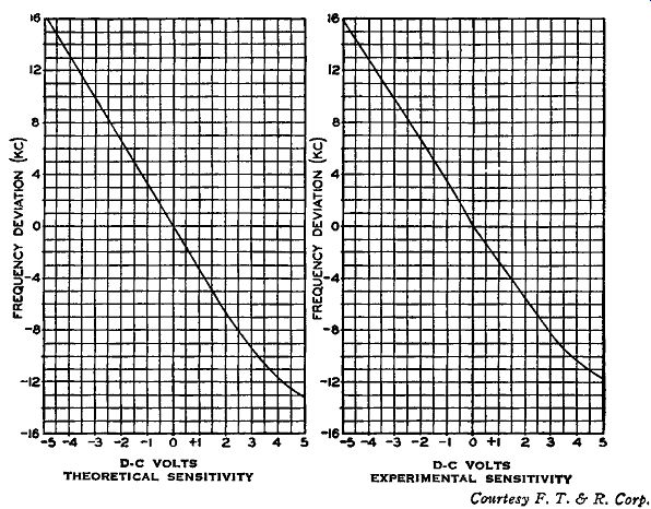
Fig. 4-27. Grid voltage, Ee, plotted against computed frequency deviation
(A) and grid voltage vs. experimental frequency deviation (B). The difference
between the calculated and experimental deviation was 8 percent.
A curve of grid voltage Ee versus computed frequency deviation is shown in Fig. 4-27 (A). This curve is a theoretical sensitivity curve in which the frequency deviation between +2 and -2 volts is approximately 13 khz, indicating the sensitivity to be 13/4 or 3.25 khz per volt. For comparison purposes an experimental sensitivity curve was also run and appears in Fig. 4-27 (B). From this curve the frequency deviation between +2 end -2 volts Ee is approximately 12 khz, showing the sensitivity to be 12/4 or 3.0 khz per volt. The percentage variation between the theoretical sensitivity of 3.25 khz per volt and experimental sensitivity of 3.0 khz per volt is found to be only 8 percent, which indicates that the theoretical curve is a good approximation.
Frequency Multiplier System
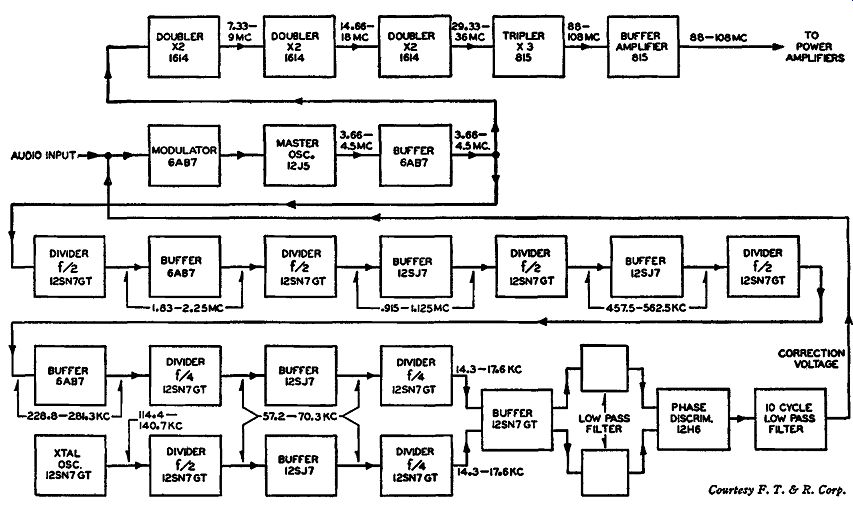
Fig. 4-28. Block diagram of the Federal FM transmitter with the power
amplifier section omitted.
In Fig. 4-28 a block diagram of the Federal FM transmitters is illustrated. It consists primarily of three sections, namely the oscillator-modulator section, the frequency multiplier section, and the master oscillator control system. The master oscillator and modulator sections have already been discussed. Let us now examine the frequency multiplier system. FM output from the oscillator-modulator circuit is passed through a 6AB7 buffer amplifier, and the FM output from this buffer is injected into a system of frequency multiplier tubes consisting of three doublers and one tripler making the total frequency multiplication equal to 2 X 2 X 2 X 3 or 24 times. Therefore, for the center frequency of transmission of 88 to 108 mhz the master oscillator frequency must lie between 88 mhz/24 or 3.66 mhz and 108 mhz/24 or 4.5 mhz. The variable inductance in the oscillator tank circuit as seen in Fig. 4-26 can be preset, so that the master oscillator can be at any frequency within the range of 3.66 to 4.5 mhz. For 100 percent modulation or 75- khz peak deviation output from the power amplifier, the peak deviation of the FM oscillator should be 75 khz/24 or 3125 cycles, no matter what the center frequency of the oscillator may be.
The last multiplication stage is an 815 tube which is used to drive the next 815 buffer which in turn is the driver for the following power amplifier stage.