We will discuss now the first local oscillator (LO) which usually is a variable frequency oscillator working directly into the first mixer of a communication receiver. Figure 1 shows a 5 MHz Vfo operating as an integral part of the 9 MHz i-f receiver we have previously chosen for our example. This Vfo can provide 500 kHz of coverage (5.0-5. MHz) allowing our receiver to tune the 14 MHz amateur band, if the first mixer operates in a subtracting mode (14- 5=9). If the first mixer operates in the adding mode (4+5=9), the 3.5 MHz amateur band can also be covered with the same Vfo (dial tuning would be reversed). Switching between the two bands would be accomplished by changing the preselector from one band to the other.
Although this technique has been used for many years, the drawback remains the inconvenience of the reversed tuning for one of the bands if a mechanical dial is used. In the case of a digital dial, this problem is greatly diminished due to the instantaneous frequency readout.
If the same direction in tuning was desired, and several other bands were required for our receiver, the Vfo would have to switch ranges as shown in Fig. 1 in order to tune all bands of interest. This technique has been widely used by many manufacturers, however, switched tuned circuits in Vfos proved to be a poor choice of design in some receivers due to dirty contacts in switches resulting in frequency instability especially at higher frequencies. Improved performance is obtained if the Vfo is mixed with fixed crystal oscillators which inherently have good stability.
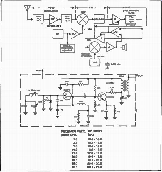
FIG. 1. Implementing a switched Vfo in a 9 MHz i-f communications
receiver
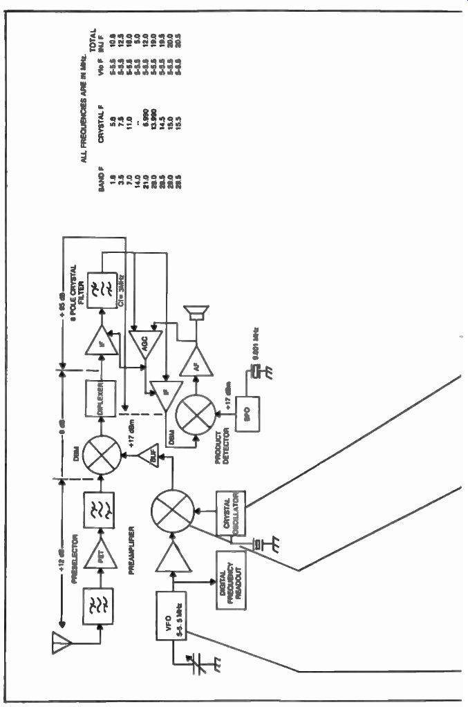
FIG. 2. Requirements for a mixed Vfo in a 9 MHz i-f communications
receiver.
MIXING VFO'S WITH CRYSTAL OSCILLATORS
In most receivers, a mixing scheme such as the one in FIG. 2, is used to provide injection to the first mixer. The Vfo operating at 5.0 to 5.5 MHz is mixed with several crystal oscillators as shown in our example. The mixing products are carefully filtered out at the output of the mixer which in our case is an active MC1596. The corresponding capacitors are automatically introduced in the transformer/filter circuit T1 by the band switch wafers SC and SD as shown. This scheme provides good results over the switched Vfo by basing most of its stability on the crystal oscillators. If a different frequency scheme is contemplated, even a lower frequency Vfo could be considered, putting most of the stability burden on the crystal oscillators. (A Vfo should be kept as low as possible in frequency, because stability can be achieved easier there). The mixing scheme should be chosen with extreme care since this additional mixing process generates a multitude of products which could interfere with the receiver's performance. A full system analysis should be performed prior to the circuit design by using the method previously discussed. It can be seen from this discussion that the plain Vfo would be preferred from a spurious response point of view, however stability problems introduced by switching, yield mixing schemes which in turn intro duce unwanted spurious products which could carry through the entire receiver. The real solution for solving the stability problem is the frequency synthesizer, but the design becomes much more complex, contrary to popular belief.
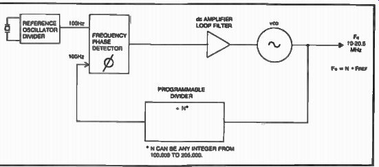
FIG. 3. A typical phase-locked loop synthesizer. Resolution is 100
Hz.
INTRODUCING THE FREQUENCY SYNTHESIZER AS A VFO
Although there are many types of frequency synthesizers, the phase lock type is probably the most widely used approach in communication receivers. It is very simple to understand in its basic form. Figure 3 shows a block diagram for such a synthesizer. This scheme could be used to generate the entire range of frequencies of 10.8 to 21 MHz necessary for the local oscillator injection in our 9 MHz i-f communication receiver example.
In this synthesizer, a reference frequency is derived from a crystal oscillator (100 Hz) and fed to one side of a phase comparator/detector. In order to make the vco operate at the required frequency, the entire loop searches until the second line to the phase detector becomes equal in phase and frequency to the reference frequency (100 Hz). It is at this point that the dc output of the phase detector (which is the control line to the voltage controlled oscillator) assures that the desired frequency is developed at its output.
The loop tracks continuously so that the stability of the output is always based on the stability of the reference frequency. If a change in frequency is desired, all that has to be done is to change the division number N and the synthesizer will search for whatever vco frequency divided by N will give a 100 Hz signal at the second input to the phase detector, (in Phase with the reference) as shown. This relationship can be expressed by Equation 1.
Eq. 1.
F = N x F ref out
Where: F oul is the desired output frequency N is the division number F ref is the reference frequency
It can be seen from this equation that the phase-locked loop approach can provide injection frequencies to the first mixer of a communication receiver in fractional steps, unlike the Vfo which provides continuous coverage within the specified frequency range.
To approach this continuous resolution, the synthesizer bases itself on the reference frequency, and can not tune continuously. The reference frequency determines the switching step, in our case 100 Hz. Every time the division number is switched digitally, a 100 Hz step is obtained which will sound just like stepping through a musical staircase generator when tuning an outside signal with the receiver (if the bfo is on). In reality, this synthesizer is not practical.
The 100 Hz reference which is needed to create the tuning resolution, would make the switching extremely slow, so that it may take approximately half a second to achieve locking, which would be a long time to retune from an operator standpoint. Secondly, the 100 Hz reference would introduce sidebands to the local oscillator which would intermix with the incoming signal and create intermodulation distortion. Thirdly, such a system would be affected by hum since the reference frequency is kept low as in our case.
PRACTICAL PHASE-LOCKED SYNTHESIZERS
The solution for fast switching is increased reference frequency. This would also put the sidebands further away from the signal, making filtering more possible. However, increasing the reference frequency would change the resolution step. In order to achieve 100 Hz resolution with higher reference frequencies, the synthesizer becomes much more complex as we will see.
MULTI-LOOP SYNTHESIZERS, A REALITY
By using two loops, or two synthesizers with slightly different reference frequencies, and by stepping them in a specific mathematical relation ship, and finally subtracting them in a mixer, fast switching and proper resolution can be achieved at the same time. By using this approach, a radio receiver can be made to scan over the entire range of interest. The cost is medium digital complexity. Figure 4 shows a block diagram approach for a dual synthesizer as applied to the 9 MHz i-f communication receiver. The two loops use separate reference frequencies which differ from each other by the resolution (derived from same source) frequency (10.000 Hz - 9.900 Hz = 100 Hz). Also shown in FIG. 4 is a small part of the tedious algebraic manipulation of the two numbers (N1 and N2) necessary to tune the receiver over a 30 kHz range from 1.000 to 1.030 MHz. Note that there are 300 individual combinations of N1 and N2 alone to cover this range. A specially designed interface would have to be used to accommodate all possible combinations of N1 and N2. The long term stability of this type of Vfo is determined entirely by the reference oscillator stability, and it can be as good as few Hz when using an oven-controlled crystal oscillator.
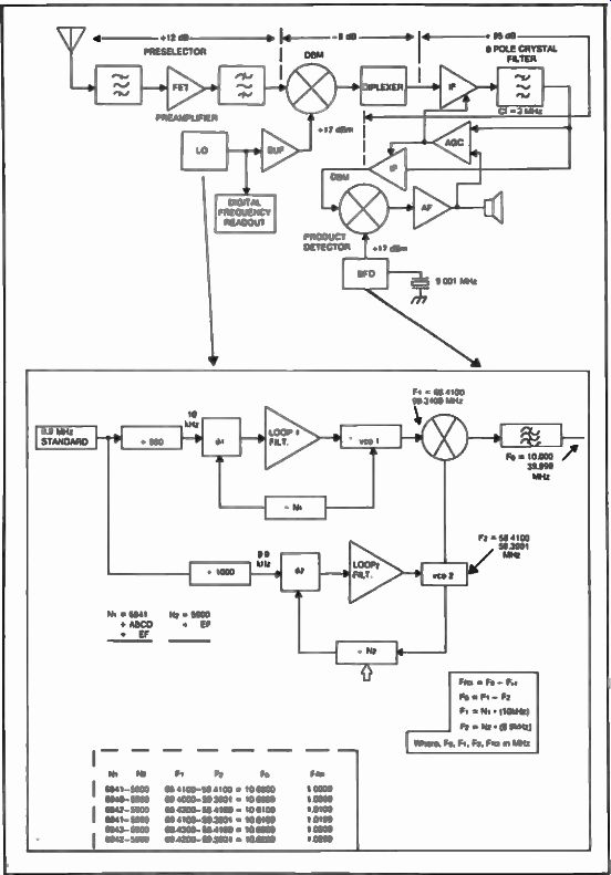
FIG. 4. Using the dual loop synthesizer in the 9 MHz i-f communications
receiver provides fast switching and high resolution.
In order for this stability to be maintained throughout the entire receiver, a similar dual synthesizer would have to be used in the place of the bfo. In this synthesizer, N1 and N2 would have such values that a 9 Mhz signal would be generated at the output. Offsetting the bfo would also be possible by changing these numbers. It is entirely possible by using this method to slave the entire receiver to the reference frequency, and this receiver would become an ideal candidate for remote controlling.
Figure 5 shows a block diagram of the reference generator which is a combination of two forms of synthesizers in itself, a brute force and a fixed phase-locked approach. By using a reference frequency of its own, the 9.9 kHz and the 10 kHz reference frequencies necessary for all loops can be derived from a typical 4 MHz, oven controlled crystal oscillator.
Figure 6 shows the schematic diagram for the digital portion of a dual synthesizer. To simplify the circuit design, the Hughes HCTR-0320 LS1 chip was used for both loops. This large-scale integration (LSI) CMOS device is equipped with a programmable divide-by-N counter, a phase/ frequency detector and an adder/decoder which provides proper interface with the digital inputs. Figure 7 shows the internal configuration of this versatile integrated circuit.
Multi-loop synthesizers are a fact of life in today's technology. As many as four or five loops are sometimes used in multi-conversion receivers. Complicated steering mechanisms provide fast switching with minimum noise problems over wide frequency ranges, while lock-up times have been reduced to milliseconds and sometimes to microseconds. See FIG. 8.
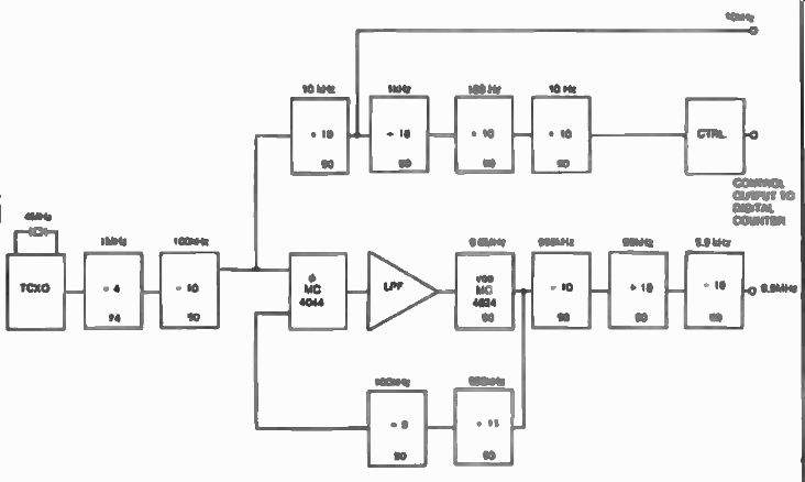
FIG. 5. Deriving the 9.9 kHz and the 10 kHz references from a 4 MHz
oven-controlled crystal oscillator. This synthesizer uses a brute-force
approach combined with a fixed phase-locked approach.
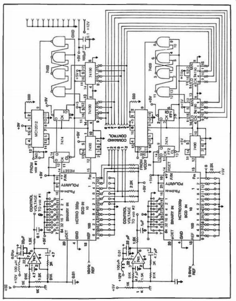
FIG. 6
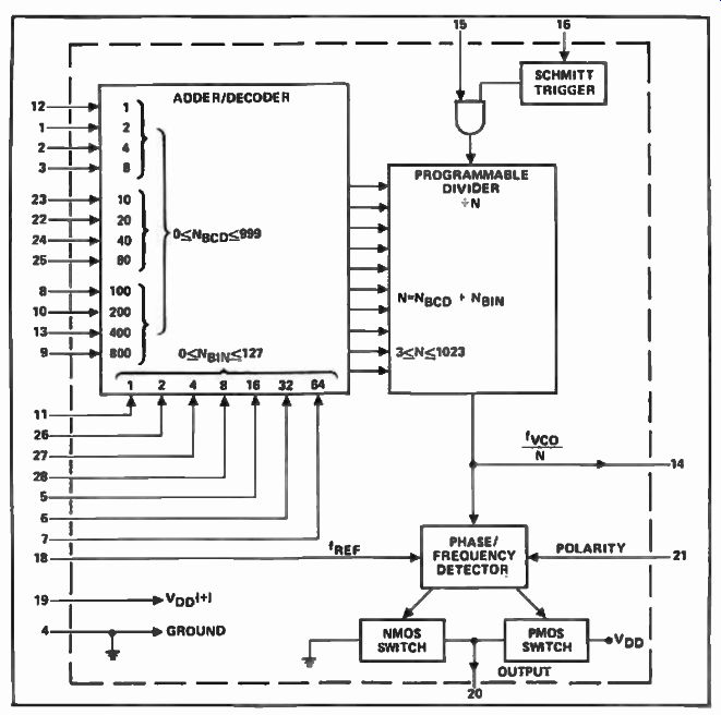
Fig. 7. Internal configuration of the Hughest HCTR-0320 LSI synthesizer
chip.
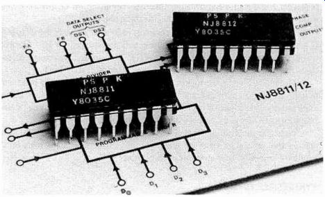
FIG. 8. Special ICs are being manufactured to provide all functions
necessary in a phase-locked loop synthesizer. The Plessey NJ 8811/12
contain a reference divider, a programmable divider and a phase/frequency
detector (courtesy of Plessey Semiconductors).
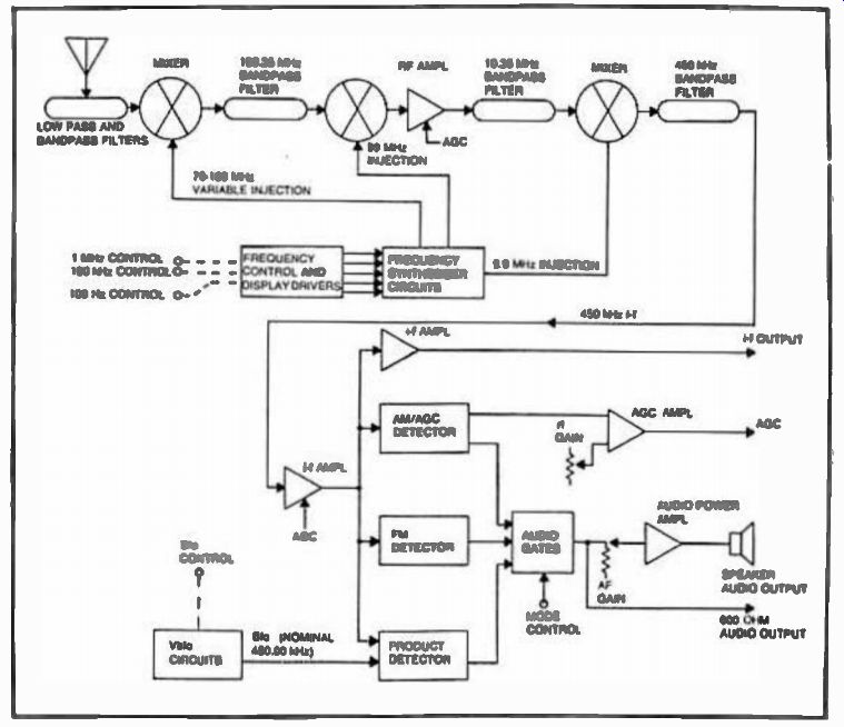
FIG. 9. Block diagram of the Rockwell-Collins 651S communications
receiver Frequency synthesizer provides all injections necessary in this
triple conversion receiver.
Figure 9 shows the block diagram of the Rockwell-Collins 651S receiver. This triple-conversion approach uses a frequency synthesizer which provides injection signals for all mixers involved. The block diagram of the synthesizer used in this receiver is shown in FIG. 10.
In this approach, all loops are slaved to a single reference frequency (9.9 MHz). The Rockwell-Collins 851S-1 shown in FIG. 11 is an even more advanced form of a multi-conversion synthesized communication receiver. Figure 12 shows the internal configuration of this receiver with the synthesizer and the digital interface shown.
The frequency stability of this receiver is 5 x 10^-7 Hz over the 0° to 50° C temperature range, and the drift rate will not exceed 3 x 10^-8 Hz per week. The lock-up time is on the order of 2 milliseconds. Typical specifications for the Rockwell-Collins 851S-1 are listed in Table 1.
The multi-loop phase-locked approach just described is only one form of implementation of frequency synthesis, but many other forms are being used today either alone or in combination with the above, depending on the requirements of the system design for a particular receiver.
To better understand what can be done in receiver design we will now discuss the several forms of synthesizers that can be used to provide local oscillator injection in communication receivers.
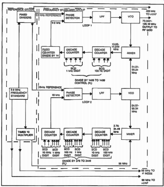
FIG. 10. Block diagram for the frequency synthesizer of the Rockwell-Collins
651S-1 communications receiver. Two loops are involved in this approach
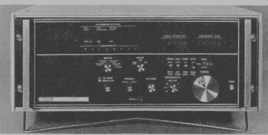
FIG. 11. The Rockwell-Collins 851S-1 communications receiver uses
an advanced synthesizer to provide fast switching for tuning (courtesy
of Rockwell International).

Table 1. Specifications of the Rockwell-Collins 851S-1 Communications
Receiver.
FIG. 12. Internal configuration of the Rockwell-Collins 851S-1 receiver
showing the synthesizer portion at right (courtesy of Rockwell International).
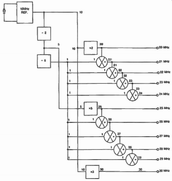
FIG. 13. An example of a direct synthesizer using dividers, multipliers
and mixers.
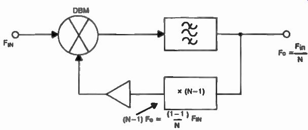
FIG. 14. Wideband analog divider using a mixer.
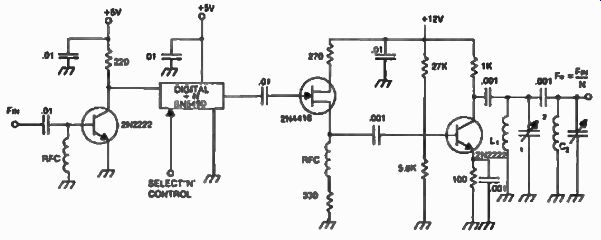
FIG. 15. Wideband digital divider using an SN 5490 integrated circuit.
( F IN MAX •< 20 MHz).
SYNTHESIZER FORMS
While a brute-force or a harmonic approach can be used for rough tuning, a phase-locked or a frequency-lock combination can be used to fine tune the receiver. The cost/performance trade-offs are usually the determining factors in choosing the right combination. Proper understanding of the advantages and disadvantages offered by the different types will help the designer to make the right decisions before implementing a system, and not after.
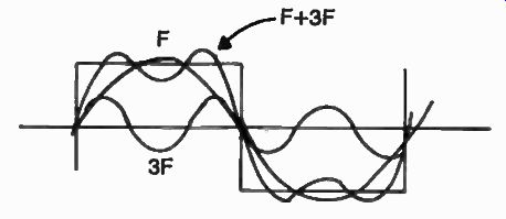
FIG. 16. The output of the wide-band digital divider contains many
odd harmonics which have to be carefully filtered out.
FIG. 17. Frequency division using the SN 5490 (7490). Any division
between 2-10 can be obtained without any additional parts.
DIRECT (BRUTE FORCE) SYNTHESIZER
The direct synthesizer uses multiplication, division, and mixing to produce desired frequencies from a reference frequency source. This type of synthesizer was first discovered in the 1940s and it usually applies to cases that require the generation of a relatively small number (up to ten) of frequencies such as in a limited coverage dual-conversion receiver in which the first local oscillator selects the rough bands to be fine tuned later in the second local oscillator. Figure 13 shows an example of a direct synthesizer that generates the frequency range of 20 to 30 MHz in 1 MHz steps. For reasons of simplicity, the extensive filtering required in this type of synthesizer is not shown in this example, however the system should be designed following the rules presented earlier because of the many pro ducts that can be generated by the multipliers, dividers, and mixers used in this approach.
Digital and/or analog techniques can be used to accomplish the functions necessary for this synthesizer. Figures 14 and 15 show typical implementation of a N circuit using analog and digital techniques. Extreme care in filtering the output of the digital approach should be observed because of the many products contained in the resulting square wave, as shown in FIG. 16.
FIG. 18. Narrow band multipliers using tuned circuits in the output
of a typical amplifier configuration. Several stages can be cascaded
to maintain signal level or provide amplification.
FIG. 19. This narrow-band frequency doubler has built-in rejection
to un wanted products.

FIG. 20. Wide-band analog doubler using a doubly-balanced mixer.
FIG. 21. Some unwanted products generated by a direct synthesizer.
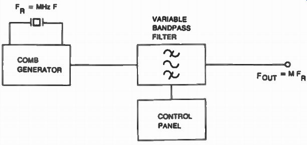
FIG. 22. Typical harmonic synthesizer uses a comb generator and a
variable band-pass filter to generate multiples of F R.
Figure 17 shows the pin configuration for implementing any division number between 2 to 10 for the SN5490 (7490) in the above circuit.
Although faster digital devices could be used, the limitation of the input frequency for this device is approximately 20 MHz. Other devices such as flip-flops (SN-5474-7474) can also be adapted to this circuit in order to perform simple divisions. Frequency multipliers are also used in brute force synthesizers. Figure 18 shows circuit implementation for a x2, x3, and x4. narrow-band multiplier using analog techniques.
Another narrow-band multiplier can be obtained with digital techniques as shown in FIG. 19. This example acts as a doubler of the input frequency, by properly selecting the time constants for the dual one-shot configuration. The same analog interface can be used here, although filtering is not as important as previously, because of the inherent harmonic rejection caused by the one-shot timing elements (approx. - 35 dB). A wide-band doubler is shown in FIG. 20. The bandwidth of this approach is limited by the frequency response of the power divider and mixer used.
In conclusion the brute-force synthesizer presents several advantages. It is relatively simple to implement if the system application is correct, and it presents fast switching which is unparalleled by any other method. The problems associated with this type of synthesizer are usually the unwanted products generated in the mixing, multiplying, and dividing process, as well as the relatively large phase noise generated by this process as shown in FIG. 21. This type of synthesizer is relatively expensive to build because of the extensive shielding and filtering required.
In spite of this, it is widely used in many receivers, from CB sets to guidance systems.
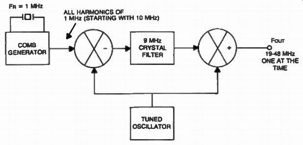
FIG. 23. Harmonic synthesizer uses tuned oscillator and crystal filter
to select harmonic frequencies.
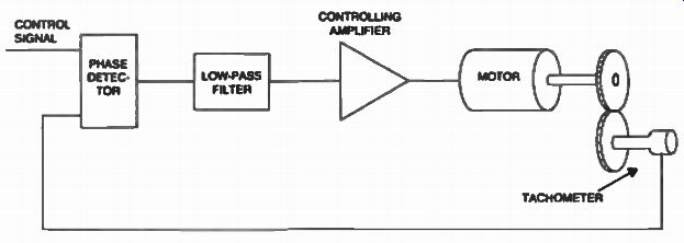
FIG. 24. Phase-lock analog with a closed-loop motor control system.
THE HARMONIC SYNTHESIZER
The harmonic approach is used whenever channel spacing between adjacent frequencies is the same, such as in a communication receiver. This approach uses the harmonic content of a reference frequency which equals the step required (usually 1 MHz). This oscillator is referred to as a comb generator because of the resemblance with a comb when the output signal is viewed on a spectrum analyzer. Each individual output can be selected with the help of a variable bandpass filter as shown in FIG. 22.
Another approach is presented in FIG. 23. In this example, there is no variable bandpass filter, as selectivity is provided by the 9 MHz crystal filter. Selection of the proper harmonic is obtained through the process of double mixing provided by the tuned oscillator.
This system can offer superior spurious performance over the previous one because of the i-f type processing offered by the crystal filter however, an image problem develops because of the heterodyne approach.
The methods presented here can be used in communication receivers either alone or in combination, depending on system requirements. A brute-force approach combined with a phase-locked approach was previously shown in FIG. 5. This combination provided two reference frequencies that were derived from one source for the dual-loop synthesizer discussed earlier. Many other combinations are also possible by using the harmonic approach.
THE PHASE-LOCKED LOOP (PLL) AND ITS ANATOMY
The phase-lock principle was discussed earlier. This approach is nothing more than a modern implementation of a closed loop motor control system as shown in FIG. 24.
A control signal of a certain frequency which is proportional to the desired speed of the electric motor is fed to one side of the phase comparator and since the phase difference between this signal and that produced by the tachometer is at the same value, the motor will be forced into syncronism at the point of coincidence between the two phases.
However simple this may seem, the application of this principle to a fast-switching phase-locked synthesizer used in a communication receiver presents a rather complex mathematical case, which is usually analyzed by Laplace transformation methods. These methods allow the designer to analyze the transient and steady state conditions, providing for evaluation of all the operating cases in a phase-locked system.
Although such detailed mathematical discussion is a must in under standing how such a system works, it is nevertheless beyond the scope of this guide. The reader is directed to special publications which will provide ample information in this direction. The bibliography at the end of this guide lists some of the works recommended for this purpose.
The basic PLL synthesizer shown in FIG. 3 contains five functional blocks.
• Reference oscillator/divider
• Frequency/phase detector
• Dc amplifier/loop filter
• Voltage controlled oscillator (vco)
• Programmable divider
We will now analyze each of the five blocks.
REFERENCE OSCILLATOR/DIVIDER AND REQUIREMENTS FOR CAUBRATORS
The reference oscillator can be called the heart of the PLL because it establishes the stability performance characteristic of the synthesizer's output. It is sometimes not more than a simple crystal oscillator. It can take the form of a highly stable, temperature controlled, frequency source which in turn could be locked to atomic standards or time stations such as WWV or WWVB. It can provide frequency accuracies as good as 1x10 12 Hz/sec.* Several forms of reference oscillators are shown in FIG. 25. Commercially available reference oscillators usually operate in the frequency range of 1 to 10 MHz. The 4 and 5 MHz models are probably the most widely used today. If stability is not of extreme importance, the designer can build his own. Figure 26 show some digital approaches to implementing this function. For higher frequencies, and sinewave outputs, Fig. 27 show how a reference oscillator can be built.
In practice, the reference oscillator frequency is further divided by digital means in order to obtain the reference frequency needed for the phase-locked loop. Figure 28 shows how a 100 kHz reference frequency can be derived from a 4 MHz commercially available temperature compensated crystal oscillator (TCXO).
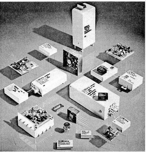
FIG. 25. Several types of crystal oscillators (courtesy of McCoy
Electronics).
['Typical short term stability specification. over the temperature range of - 55°C to +129. c. Long-term stability - 10 of ±5n 10 Hs/day have been achieved for the same temperature range with proportional ovens.]
In a communication receiver, a reference oscillator can also serve another function if the receiver is not synthesized. It can be used as a time base for a digital counter used for measuring the tuning frequency, or with some slight modifications it can serve as a frequency calibrator for a receiver with an analog dial.
The calibrator is usually equipped with a 100 kHz crystal oscillator.
The output of this oscillator is coupled with the receiver's antenna and the harmonics generated by the oscillator appear every 100 kHz within the receiver's tuning range at different points of the dial, allowing for calibration. Figure 29 shows a simple implementation of a frequency calibrator using the Motorola MC4024. This chip contains two independent vco's. Our design uses the spare one to provide pulsed 100 kHz bursts which can be easier identified than a continuous carrier at the output of the receiver.
Figure 30 shows a more elaborate calibrator which can be pulsed or continuous and it can also provide 10, 20, and 50 kHz calibration signals as well as the 100 kHz signal. Selection of these frequencies can be obtained with the use of the S 1 A, B, C switch. This design offers considerable flexibility as only one IC is used to accomplish the different frequency divisions.
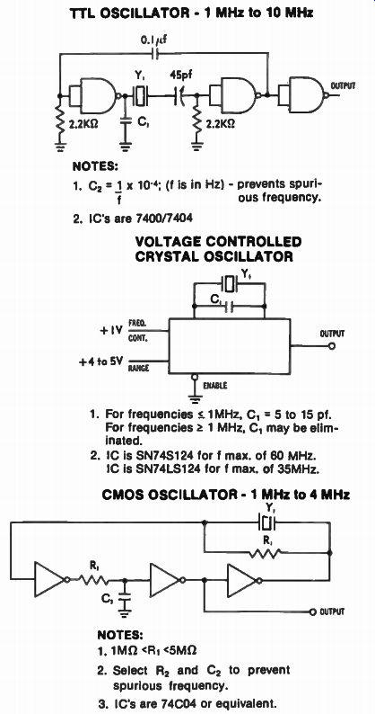
FIG. 26. Digital implementation of reference oscillators.
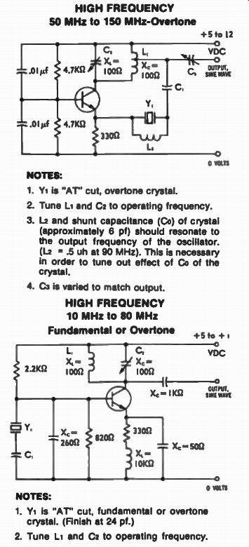
FIG. 27. Analog implementation of reference oscillators for the frequency
range of 10 to 150 MHz.
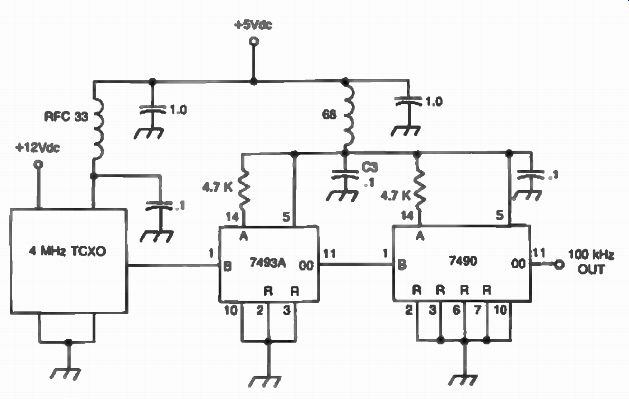
FIG. 28. Obtaining 100 kHz reference frequency from a 4 MHz TCXO.
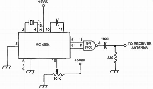
FIG. 29. Pulsed 100 kHz signals can be used to calibrate a communications
receiver.
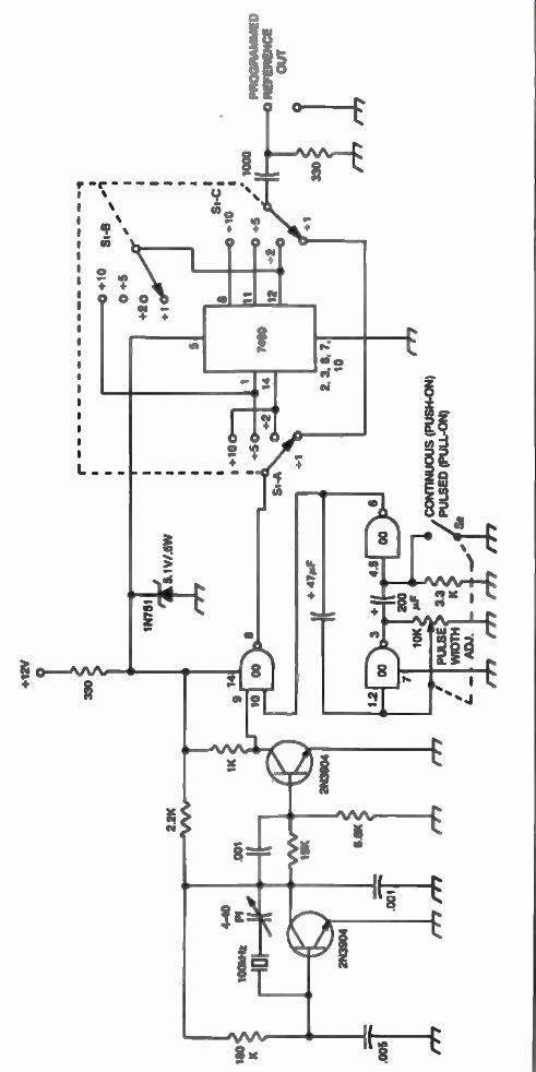
FIG. 30
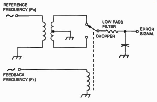
FIG. 31. Phase detector mechanical analogy.
PHASE DETECTOR
An element necessary in the design of a phase-locked loop is the phase detector. It is considered the brain of the system because it senses errors and outputs proper commands to the vco in order to lock to the reference frequency. The phase detector, or as it is sometimes called, the frequency/phase comparator uses the reference frequency to compare against the signal from the vco, as modified by the programmable dividers, and outputs a dc signal to the vco proportional with the correction necessary to bring it to the required frequency. To better understand how the phase detector works, consider the electromechanical analogy illustrated in FIG. 31.
As the chopper switches between the two sides of the transformer at the feedback frequency rate, the reference signal appears at the armature alternately at 0° or 180° phase points. If the reference signal ( F R) and the feedback signal ( F E ) are not equal in frequency, the armature will actually see the sum and the difference of the two signals (FR+FF) and ( F R- F F ) making the circuit act much like a mixer. The lowpass filter will reject the sum (Fm+FF ) allowing only the difference ( F R- F F) to pass through with increasing amplitude as the reference frequency is approached by the feedback frequency. When the two are exactly the same, a positive dc voltage is generated as the error signal. The level of the signal is directly proportional to the phase difference (0) between the two signals. This value is usually expressed in electrical degrees as shown in Equation 1.
t 2 - t = x 360° Eq. 1
Where: each is the phase difference in electrical degrees, t 1 is the event time in seconds from the start of one cycle on the reference frequency, t 2 is the corresponding event time expressed in seconds in the feedback signal, and T is the total time required for one cycle (360°) of the reference frequency.
Looking at FIG. 32, the reference frequency ( F R ) has a cycle time (T) equal to 1.8 seconds. The event point (t,) was chosen to be on the rising edge of FR and is equal to 0 seconds. The corresponding edge of the feedback frequency t 2 is delayed by 0.3 seconds, as shown.
Then: ,à 43 - 0.3 x (36e) - (13 x( 360 `1= 60° 1.8 1.8
It can then be said that the reference frequency in this example leads the feedback frequency by 60°, or that the feedback frequency lags the reference frequency by the same amount. In a practical phase-locked loop, the error voltage generated by the phase detector is dependent on this value, as shown by Equation 2.
V0 = Kçb x .10) --- Eq. 2
Where: V. is the average output voltage of the phase detector in volts, KO is the phase detector conversion gain in volts/radian, and tie is the phase difference expressed in radians. (1 radian=180°/r= 57.295)
Practical phase detectors may be implemented using digital technology. Shown in FIG. 33 is an Exclusive-OR approach using the 5486 (7486) integrated circuit. This type of phase detector is usually used for input wave forms with a 50% symmetrical duty cycle. Flip-flop functions are also common to phase detectors as shown in Figs. 34 and 35. The 5474 (7474) dual flip-flop is used in these examples.
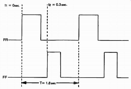
FIG. 32. Calculating the phase difference (0) between two signals
FR and F F.
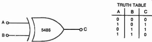
FIG. 33. Exclusive OR phase detector using the 5486.
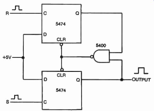
FIG. 34. U sing flip-flops in a phase detector.
These methods are sensitive to harmonic multiples of the feedback frequency, and also if the duty cycle changes on either input, erroneous locking can result. To avoid these inconveniences, special phase detectors in IC form have been designed by various manufacturers. Figure 36 shows the diagram of the Motorola MC4344 (4044), which consists of two digital phase detectors, a charge pump, and an amplifier. Phase detector 1 is intended for systems using negative edge triggered circuitry, where zero frequency and phase difference are required at lock. The total transfer characteristic curve of phase detector 1 (with the charge pump connected) is a sawtooth with a wide linear range of 4 radians as shown in FIG. 37.
Typical conversion gain (K phi) for this detector is 0.12 volts/radian.
Phase detector 2 is connected in parallel with phase detector 1, and can be used if quadrature lock is desired. Its outputs can also be used to drive a lock indicator for phase detector 1. Figure 38 shows the circuit diagram for both detectors with corresponding timing diagrams.
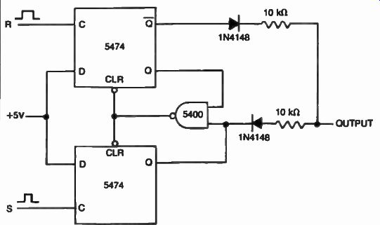
FIG. 35. Another approach to flip-flop phase detectors.
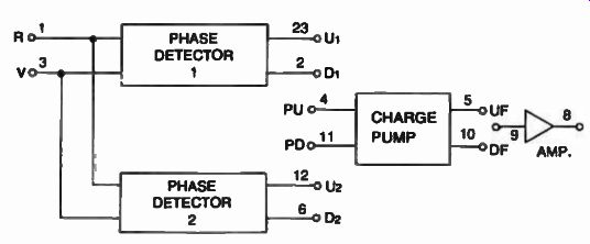
FIG. 36. Block diagram of the MC 4344 phase detector.