AMPLIFIER/LOOP FILTER TRADEOFFS
If phase detector 1 was used, as is usually the case, loop lockup occurs when both outputs U1 and DI are high. Otherwise, a pulsed waveform will appear on either one of the outputs depending on the phase-frequency relationship of R and V.* These outputs are usually fed to the self-contained charge pump which is an integral part of the MC4344, as discussed earlier.
The pulsed waveform present on either PU or PD (pump up or pump down) will make the charge pump generate the right voltage in the proper direction for phase differences between R and V inputs of -± 2 pi radians as previously shown in FIG. 37.
[(Because of the sequential logic characteristic of phase detector 1. many logic states can be observed at U , and D1. For a better understanding of this phenomenon, the reader is directed to the Motorola Phase-Locked Loop System Data Rook which gives a complete flow table.) ]
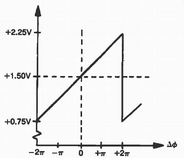
FIG. 37. Transfer characteristic for phase detector # 1 of the Motorola
MC 4344.
This figure shows that a "no pump" condition is achieved with a phase difference (à0) of zero pi radians corresponding to an output voltage at UF and DF of 1.5 volts, which is the lock-up condition. It is this output that is used to further steer the vco in the right direction. Ideally, this signal should be a fast "sliding", pure dc voltage, in order for an inherently good vco to remain clean from a phase-noise point of view.
In reality, this signal is made of a multitude of ac signals and a dc component. The high frequency components are generated in the digital part of the phase detector. The charge pump can also add noise components to the output. In order for the phase-locked loop to perform properly, a loop filter is introduced between the output of the phase detector and the vco's input. This low-pass arrangement, has the role of suppressing ac components from the output of the phase detector while still maintaining the response requirement for the entire phase-locked loop. This contradictory requirement, usually, calls for a design having a loop response at about 1% of the reference frequency.
For example, if a 10 kHz reference was considered because of fast switching requirements, the 3 dB cutoff point would be 100 Hz, meaning that the noise performance of the vco can be improved only between 0 to approximately 100 Hz, leaving all other ac components to pass through and appear as sideband noise in the output of the vco. One of the worst problems encountered in such a system is the feed-through of the reference frequency and its harmonics which appear as angle modulation sidebands on both sides of the vco's output as shown in FIG. 39. These sidebands, if not filtered, are about 40 dB down from the fundamental vco output and are located on either side by the amount of the reference frequency and its harmonics. They can contribute to the total intermodulation distortion and greatly hamper the performance of a communication receiver.
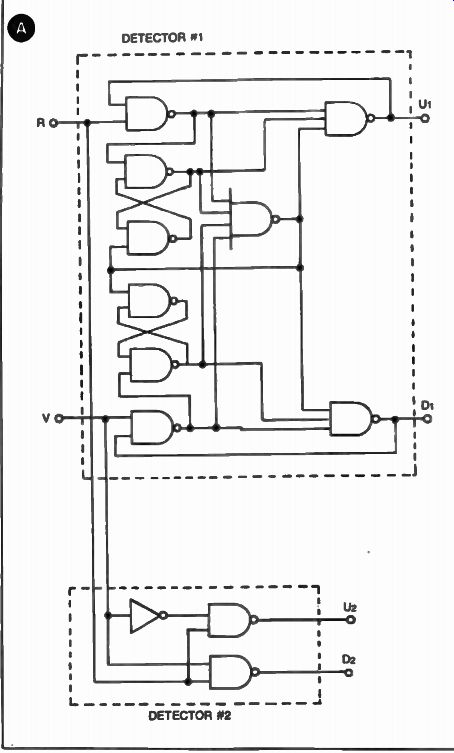
FIG. 38. Circuit and timing diagrams for detector #1 and #2 of the
Motorola MC-4344 (4044). Detector 1 and 2 (A). R signal leads V signal
(B). R signal lags V signal (C). Output at detector 2 under lock condition
(R signal in phase with V signal), and out of lock condition (R signal
leads V signal) (D).
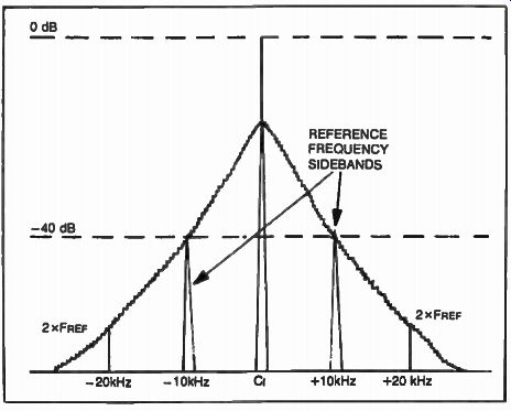
FIG. 39. Spectrum analyzer representation of a PLL's output with
reference frequency feed-through at 40 dB below fundamental.
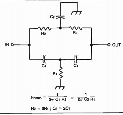
FIG. 40. The "r notch network can be introduced in the loop
of a PLL to reduce reference feed-through at the output of the vco by
40 dB.
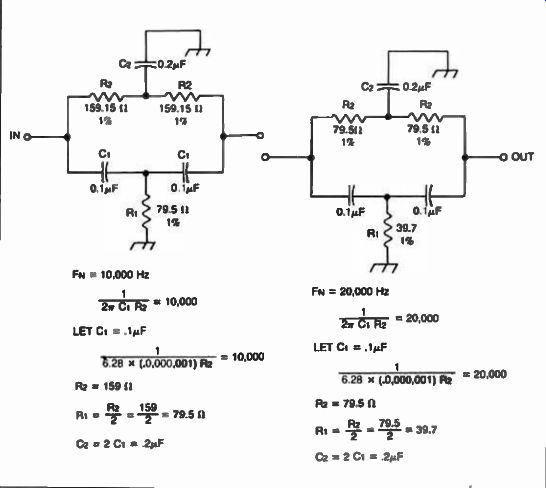
FIG. 41. Twin "T" networks used with a 10 kHz and 20 kHz
reference frequency. 40 dB of attenuation is obtained with this arrangement.
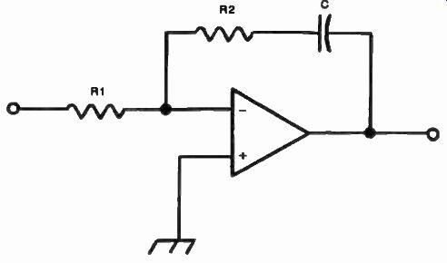
FIG. 42. A typical inverting low-pass filter using an operational
amplifier is used for the loop filter in a PLL.
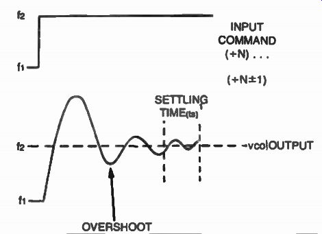
FIG. 43. Transient response of a phase-locked loop.
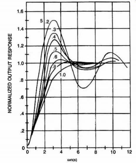
FIG. 44. Normalized transient response for a second-order system.
The twin-T notch network, shown in FIG. 40 will provide an additional 40 dB attenuation for the reference frequency or its harmonics, if introduced in the output of the phase detector. This filter is usually customary in order to reject both the reference frequency and its second harmonic.
Figure 41 shows two twin-T networks tuned to the 10 khz reference frequency and its second harmonic at 20 kHz.
The loop filter, is also responsible for the phase-locked loop's characteristics, such as capture range, bandwidth, lock-up time and transient response. This filter is usually of the low-pass active design as shown in FIG. 42. Its cutoff frequency is expressed by Equation 2.
1 coLPF(RAD/s) = R C
--- Eq. 2
Where: coLPF is the cutoff frequency for a lowpass filter.
The loop natural frequency and the damping factor can be found from Equation 3 and 15 .
n (RAD/ s = (KO Ko LPr (- RC e= cen
--- Eq. 3
--- Eq. 4
Where: con is the loop natural frequency,
KO is the phase detector conversion gain in volt/rad.,
K is the vco conversion gain in rad/sec/volt
4* is the damping factor.
The total transient response of the phase-locked loop is controlled by this filter. Upon a change in command (÷ N) the loop will search until the vco travels from one frequency F1 to the other frequency F 2. This shifting is not encountered suddenly, but when frequency F2 is reached the output of the vco will oscillate around its value until finally settling down as shown in FIG. 43.
The time that has passed between the given command and the output of the vco to settle within some certain limits (e.g. within 10% of F 2) determines the switching speed of the phase-locked loop and is usually referred to as the lock-up time.
The amount of damping determines how fast this process is completed. In designing a fast-switching synthesizer for a communication receiver, Fig. 44 should be used for determining the value wn for a given damping factor in order to apply it in the low-pass equations presented earlier. A rule of thumb in using this graph would be to design for a certain amount of overshoot within a given settling time.
Another factor controlled by the loop filter is lock-in range (wc). With the filter shown in FIG. 42, Equation 5 can be used to find this value:
= co1 ( R2 n 1 (11C --- Eq. 5
Where: wc is the lock-in range in radians/sec, and w1 is the hold-in range in radians/sec* From a practical standpoint, many designers prefer not to use the charge pump contained within the MC4344 because of its noise contribution to the 'co's output. While still using phase detector 1, they build their own.
Figure 45 shows how this can be implemented.
[** Defined as to how far the input frequency to the phase-detector can deviate from a given veo frequency. wo. This number is numerically one half the lock range.
** Modern design of Frequency Synthesizers, Ulrich L. Rohde. Ham Radio. July 1976. ]
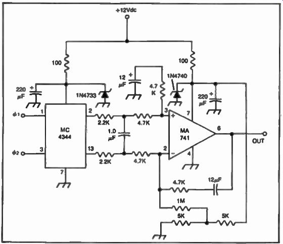
FIG. 45. The Motorola MC-4344 is used in this example without the
charge pump in order to keep output free of transients.
Other designers ** prefer the RCA CD4046. This CMOS device operates as a positive-edge-triggered digital memory network with a field-effect-transistor (FET) output stage. The phase noise contribution from this phase detector is claimed to be somewhat superior to that of the MC4344 equipped with the charge pump. Because of its low-current characteristics the CD4046 is an attractive choice for certain commercial applications. In most military applications, the MC4344 remains the work horse of phase comparators.
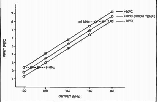
FIG. 46. Linearity of a well-designed you over the temperature range
of -50°C to +50°C.

FIG. 47. Block diagram of a basic voltage controlled oscillator.
THE VOLTAGE CONTROLLED OSCILLATOR (VCO)
The next circuit required in a phase-locked loop is the voltage con trolled oscillator (vco). This circuit takes the voltage commands from the loop filter and outputs the required sinewave frequency necessary for the receiver's conversion. This signal is also used to feed the programmable counters which in turn, close the loop at the second input to the phase detector as we previously discussed.
Ideally, the voltage controlled oscillator supplies an output frequency directly proportional to its input dc voltage control over the required temperature range. Figure 46 shows test results of the linearity over the temperature range of -50° C to +50° C for a well-designed vco. This performance was measured with a free-running vco whose input voltage was supplied by a programmable power supply that can generate precise dc voltages. It can be seen from this discussion that the vco can be referred to as a voltage-to-frequency converter (FIG. 47).
Its transfer function characteristics can then be expressed by Equation 6.
ca = K. V f o
Where: co is the vco output in rad/sec.
o V r is the vco control voltage provided by the loop filter K is the vco conversion gain in rad/sec/volt. o
--- Eq. 6
The output frequency expressed in Hz is given by Equation 7.
(t) f = ° 2 pi
Where: f o is vco frequency in Hz co is vco frequency in rad/sec 0 77» = 3.14
From a practical standpoint, the vco much resembles Vfo technologies, with the tuning being achieved through the use of voltage-variable capacitors (varactors) in the oscillator tank circuit. Low-noise vco's can be designed today by using field-effect transistors, if frequencies do not exceed 500 MHz. For higher frequencies, bipolar transistors and GaAs FETs are being used.
Often, the frequency range requirement over which a vco has to perform is extremely wide, with the result that it would take a long time for the loop to lock. This search would also be accompanied by extensive phase noise even after the loop has settled. This noise would be transferred into the receiver's circuits, accounting for serious intermodulation distortion problems and creating the so-called blocking phenomenon.
Some designers use several limited-range vco's which are automatically switched in by complex digital circuitry. A block diagram example of this approach is shown in FIG. 48. A better method of achieving low noise operation over a wide frequency range is shown in FIG. 49.
In this example, the correct vco is selected in rough steps of 1 Wiz by using a digital-to-analog converter, which brings the loop into the required frequency excursion, speeding the final lock-up process, and improving the noise performance of the system. This method has been used extensively by manufacturers and offers good results from a noise standpoint.
A less expensive method of achieving coarse steering and low-phase noise performance in a vco is shown in FIG. 50. In this example, limited frequency ranges are switched into the tank circuit of the vco by placing the selected capacitance across it. The switching is accomplished under micro-computer control with the use of PIN diodes used as current controlled switches. The Hewlett/Packard HP 3081 diode is used in this example.
Similar results can be obtained by switching inductors instead of capacitors. Either technique can be implemented by building a printed circuit board which will contain a bank of tuned circuits together with their switching mechanisms which could include the digital decoder. Because of the low Q requirements for the inductors, they could be etched directly on the board providing an economical means of production. Figure 51 shows the principles behind creating a film inductor bank in a phase-locked loop.
--- Eq. 7
Equations 8, 9, 10, and 11 show how to approximate the inductance in such an approach.*
[*Designing Inductors for Thin-Film Application, H.G. Dill, Electronic Design, Vol. 12, No. 4, pp., 52-59; 1964. ]
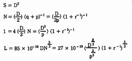
--- Eq. 8 --- Eq. 9 --- Eq. 10 --- Eq. 11
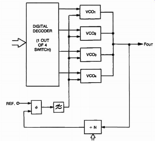
FIG. 48. This method of switching vco's in a I'LL allows superior
noise performance, but is expensive.
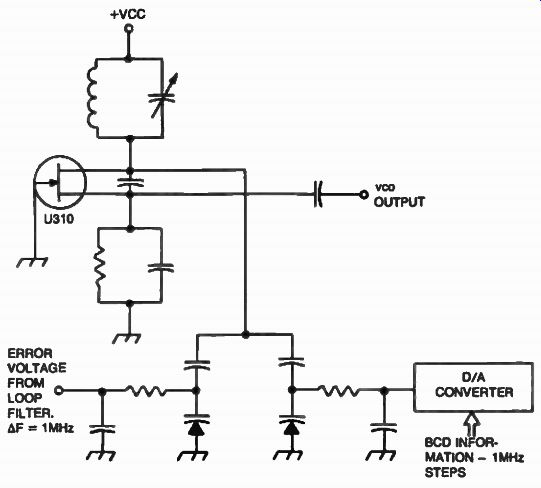
FIG. 49. Method of steering a vco by using a D/A converter.
Where: D is dimension in cm, Sis surface area of coil (D,=0), N is number of turns, L is inductance in henries, 1 is length d spiral in cm., p is spiral width in cm., and q is distance between the outer edges of two adjacent spirals.
P _ - r
Shown in FIG. 52 is the schematic diagram for a vco using film inductors in order to accomplish coarse steering. Such a design exhibits a typical power spectral density of 120 dBm/Hz at 1 kHz from the main carrier. This noise can vary however, and is highly dependent on the layout of the circuit. This is one of the reasons why the actual implementation of such a vco is usually considered a proprietary matter by the manufacturers.
Creating film capacitors on a printed circuit board has been also implemented with similar techniques, although not as often as the film inductor.
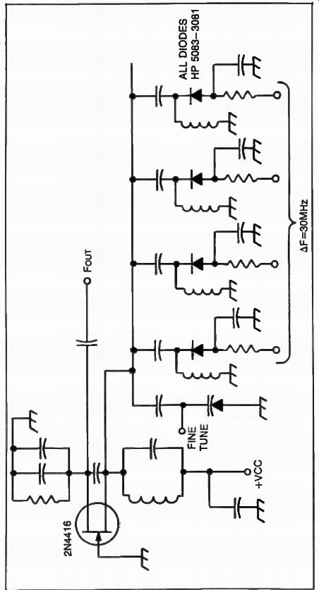
FIG. 50. A very low-noise oscillator, over a wide range can be obtained
with automatic switching of capacitors across the tank circuit of a vco.
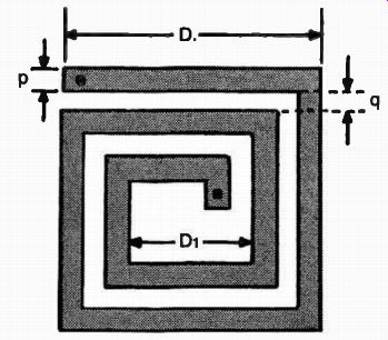
FIG. 51. Creating a film inductor for the steering mechanism.
Practical vco's take many forms. Figure 53 shows a basic FET approach using two 2N4416 transistors followed by a 2N5179 buffer amplifier. This vco will tune the frequency range of 110 to 165 MHz. The layout of the tank circuit can greatly influence this range. The harmonic content of this vco is shown in FIG. 54. No output filtering was used to obtain this information. A simple lowpass filter can reduce these harmonics by at least 20 dB making the vco's output extremely clean from a harmonic standpoint. See Figs. 55 and 56.
Integrated circuits intended for use as vco's are available from manufacturers. Figure 57 shows a circuit implementation for the Motorola MC1648. In this example, a very wide-range (3:1) varactor is used to achieve a total coverage of 30 MHz. A buffer amplifier is also shown. This amplifier is required to condition the ECL level of the MC1648 to the TTL level necessary to feed the programmable dividers which close the loop in a PLL. Although the simplicity of such a vco is quite obvious, IC vco's are seldom used in communication receivers.
THE PROGRAMMABLE DIVIDER AND THE DUAL MODULUS APPROACH
The remaining circuit function requirement for a phase-locked loop synthesizer is the programmable divider. Its function is to provide the right count to the phase detector so that the output of the vco will be the correct frequency according to the PLL equation ( 1) presented earlier. It can be seen from this equation that the step resolution of the PLL depends on the division number N. In a phase-locked loop synthesizer, this arithmetic function is performed with the help of digitally programmable dividers.
These devices accept the vco's output (once it is transformed to a square wave) and divide it by a predetermined value (N) which can be controlled by the operator at the programming inputs. Figure 58 shows the schematic diagram of the 54192 (74192) used in this function.

FIG. 51. Creating a film inductor for the steering mechanism.
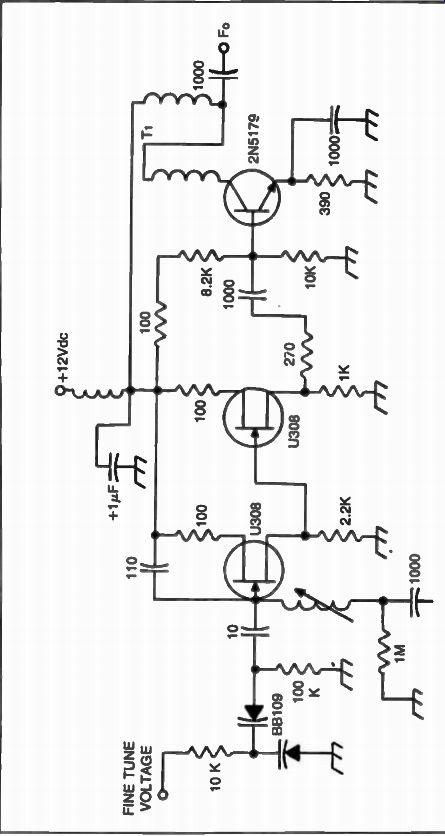
FIG. 52
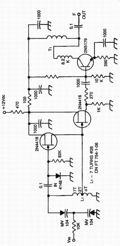
FIG. 53. Schematic diagram of a vco using two FET's and a transistor.
Frequency range is 110 to 165 MHz
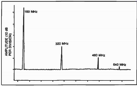
FIG. 54. Spectral purity of the vco shown at A, indicate that the
second harmonic is 38 dB below the fundamental, the third harmonic is
48 dB below, and the fourth harmonic is more than 50 dB below the fundamental.
No filtering was used at the output of the vco in making the test measurements.
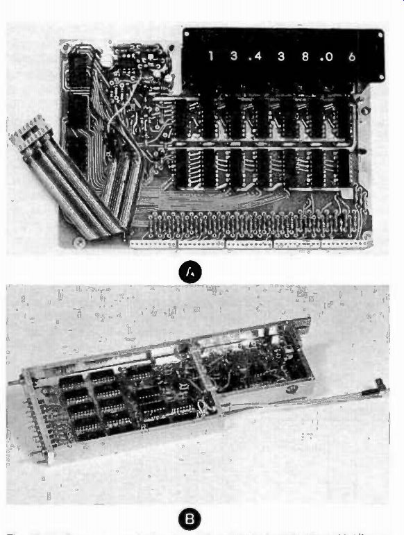
FIG. 55. Frequency control module (A) and typical synthesizer (B)
(shown with cover removed) of the Cubic HF-1030 communications receiver
(courtesy of Cubic Communications).
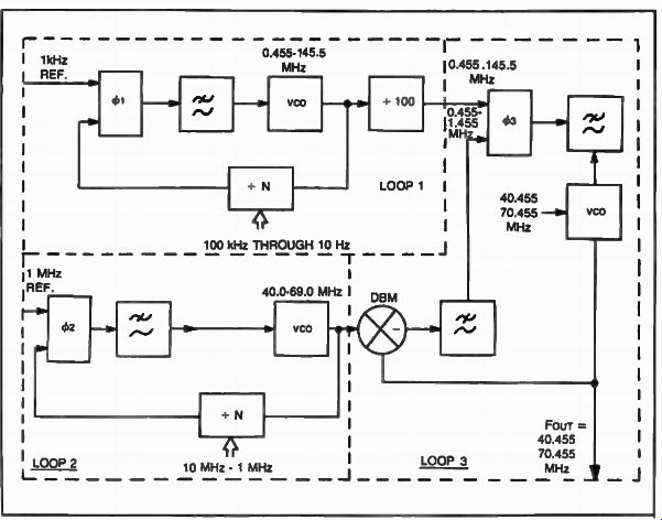
FIG. 56
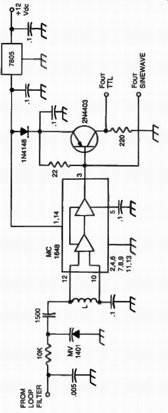
FIG. 57.
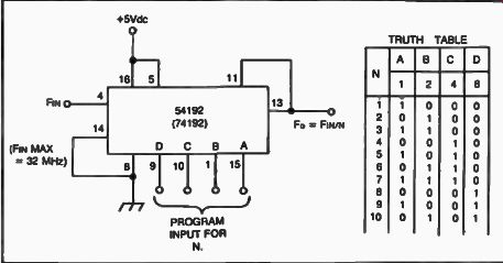
FIG. 58. Any division between 1 and 10 can be achieved with the programmable
divider.
The modulus N is implemented by making true (positive logic level equals 1) the binary weighted inputs A, B, C, and D as shown by the truth table. For numbers larger than 10, more devices can be cascaded as shown in FIG. 59. This arrangement shows three 54192's cascaded and programmed to divide by N=239. The programming is accomplished by a thumb-wheel switch which is a mechanical memory device that can directly output a binary number on four lines for each decimal number selected by the operator (N. = 999). Figure 60 shows such a switch as used in a communications receiver.
Other dividers can also be used to create divide-by-N functions. The Motorola MC4016 is such an example. This IC was expressly created for phase-locked loop circuit applications. Figure 61 shows the implementation of a programmable divider with this IC. Although somewhat simpler to use than the 54192, the MC4016 will accept a maximum frequency of only 8 MHz at its input, lithe vco's frequency exceeds the input frequency of the divider chain, a prescaler has to be used. The prescaler would also have to be a programmable counter which will accept the vco's output, sometimes in uhf frequencies. Because of technological drawbacks, programmable devices have not yet been fabricated for uhf operation. The solution to this problem is to combine the properties of a high-speed fixed counter with the functional properties of the slower programmable counter. This device is referred to as the dual-modulus prescaler and the technique used in implementing it was named the pulse swallowing technique*. A PLL Synthesizer using this approach will therefore be referred to as a dual-modulus prescaler-PLL synthesizer. To understand this technique, refer to Fig. 62 and the following explanation.
Assume that an output frequency (F„ ) of 150.020 MHz is expected with a reference frequency of 5 kHz.
From the phase-locked loop equation
( 1): F = FR X N, F 150.020 x 10⁶ Hz N - ° F R 5 x 10³ Hz - 30,004
Assume the dual modulus values P and P+1 are the numbers 20 and 20 + 1 = 21' if N is divided by the P modulus, the resulting quotient is the n program value and the A program value is the remainder.
N 30,004 = 1500 and a remainder of 4 20 n = 1500 and A = 4
The key to the operation of this synthesizer is the P + 1 function of the dual-modulus prescaler. If the above values for n and A are programmed into the synthesizer as shown in FIG. 62 the loop will perform in the following manner.
[This choice is arbitrary and depends 011 the type of device available.]
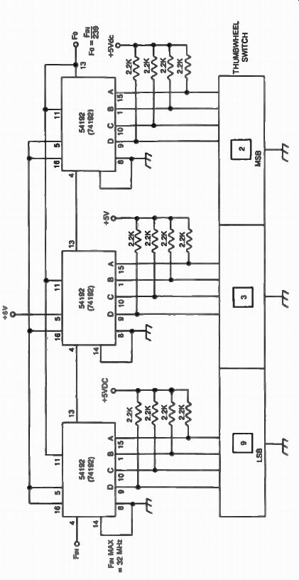
FIG. 59. Implementing a divide-by-N r -i 239 with the 54192 IC.
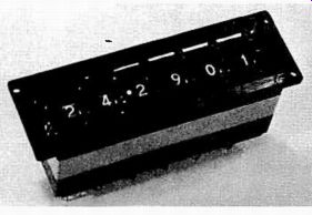
FIG. 60. A thumbwheel switch can be used to program the programmable
divider in a phase-locked loop.
The P/P + 1 divider is initially set up to divide by 21 and will output a pulse to the divide-by-n counter as well as to the divide-by-A counter for every 21 pulses it receives. Since divider A is programmed to divide by 4, this cycle will continue for another three times (each cycle equals 21 vco pulses at the P/P + 1 counter), at which time divider A outputs a command (count of four) to the control logic which instructs divider P/P + 1 to change the divisor to P = 20. Upon execution of this change, the control logic outputs an inhibit signal back to the divider A, preventing it from any further count until the total cycle is repeated. Meanwhile, divider n which has already counted to four, continues to receive pulses from divider P/P + 1 at a ratio of 20 : 1. After the remaining 1496 pulses have been received (1500-4), divider n finally outputs a pulse to the phase comparator as well as to the control logic which resets all counters and the process repeats.
It can be seen from this explanation how the "swallow" terminology has been chosen to describe this technique. To verify the mathematics involved in this example, we'll use the following equation:
N = (P + 1)A + (n - A)P N = 30,004 as found previously
. . 30,004 = (21 x 4) + (20 x 1496)
--- Eq. 9
This method allows direct programmability over the entire range of a vco operating at frequencies beyond the capabilities of conventional non prescaled counters. Devices are available today which allow other dual modulus (P/P + 1) divisions as shown in Table 2.
Figure 63 shows the circuit implementation for a 650 MHz, fully programmable dual-modulus prescaler that could be used between a vco with such frequency characteristics and a phase detector. This circuit uses the Fairchild 11C90 integrated circuit which is a + 10/11 prescaler. The up-counter should be of the ECL type in order to allow for ultra-high frequency operation.
Figure 64 shows a similar prescaler which uses the Fairchild 951190, a similar + 10/11 dual-modulus prescaler which allows operation to 250 MHz. Schottky TTL Logic (93S10) was used following the device in order to reduce the delay at the PE input. Other similar prescalers are also available from manufacturers such as Motorola and Plessey.
OTHER CONCEPTS IN SYNTHESIZERS
There are several other concepts of frequency synthesis used today.
Some are derived from the phase-lock approach, while others are frequency-lock techniques, as well as digital techniques.
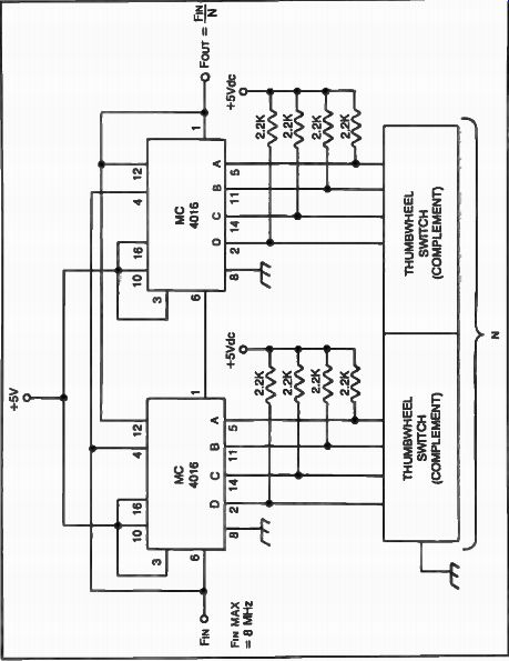
FIG. 61
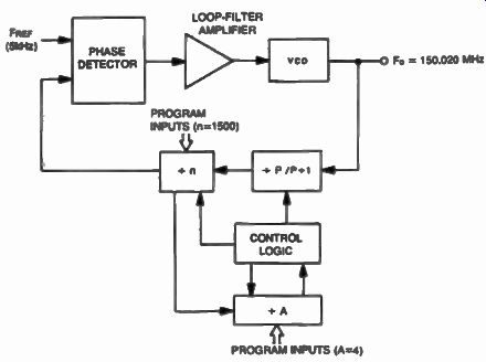
FIG. 62. The dual-modulus prescaler approach
THE MIXER PLL SYNTHESIZER
Table 2. Other Dual-Modulus (P/P+1)
Values Can Be Obtained in IC Form from Semiconductor Manufacturers.
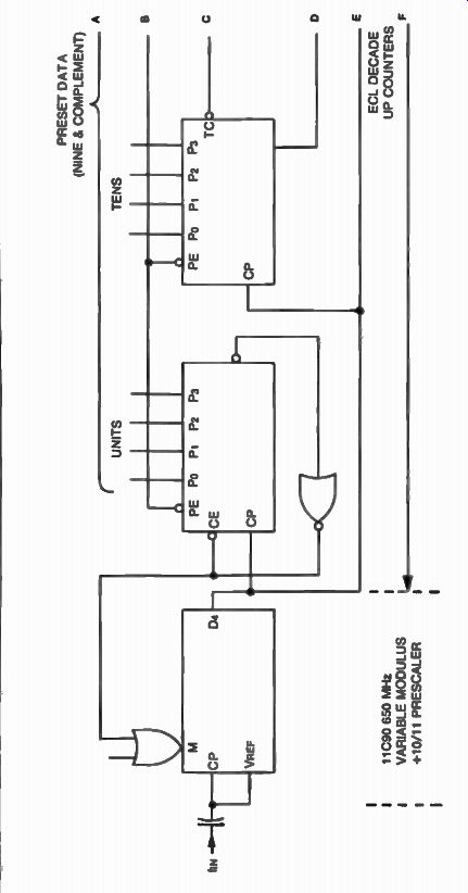
FIG. 63. Circuit diagram for a 650 MHz dual-modulus prescaler using
the 11 C 90 dual-modulus pres
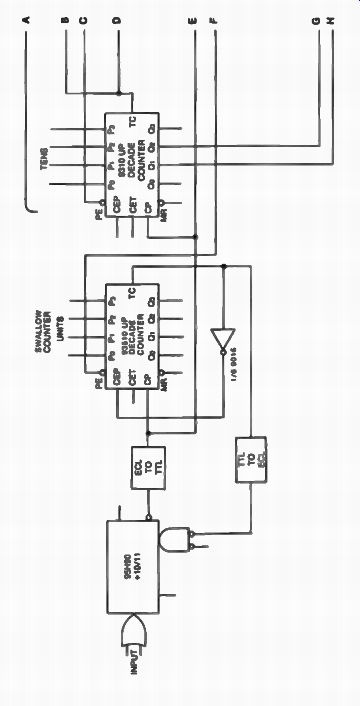
FIG. 64. A 250 MHz implementation using the 95H90, 10/11 presc
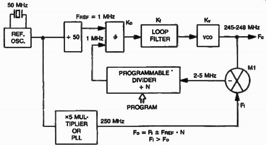
FIG. 65. Mixer PLL synthesizer block diagram.
When the dual-modulus prescaler approach is not economically practical, or the frequency of the vco is so high that there is no digital component available to perform this function, as in the case of microwave synthesizers, the mixer phase-lock technique is usually used, as shown in FIG. 65.
This approach allows the operation of the 'co at frequencies, several order of magnitude higher than the speed capability of the programmable divider, providing for inexpensive parts to be used in this part of the system. In a communications receiver, this advantage is two-fold due to the inherently quiet nature of the CMOS counters that can be used in this type of synthesizer.
Referring to FIG. 65, the vco's output operating at vhf or uhf frequencies is mixed in M1 with the fixed frequency F i which is usually greater than the maximum frequency of the vco. This injection frequency can be derived by means of frequency multiplication of the crystal controlled reference oscillator. Another way to obtaining this frequency would be to use a fixed I'LL which is locked to the same reference. The output of the mixer which operates in a subtracting mode is fed to the programmable divider, and the loop is finally closed at the phase detector.
It can be seen from this discussion that the N is reversed by the mixing process so that it changes (increases) in the same direction as Ky, greatly improving the loop dynamics (reducing con variations over the loop range). The disadvantage of this concept is the necessity of providing another signal, and also the common intermodulation problems associated with the mixing process, which can be transferred to the vco's output.
THE DIGIPHASE SYNTHESIZER AND THE FRACTIONAL N APPROACH
The problem of achieving high resolution with relatively high reference frequencies in a PLL has been discussed in the previous paragraphs.
Because the reference frequency dictates the frequency interval in such a system, relatively low frequencies would have to be used. However, such an approach proved to be impractical, and complex multi-loop PLL synthesizers resulted. It is possible to build a synthesizer capable of resolution much finer than its reference frequency.
If we consider the system in FIG. 66, an accumulator increases its number ( NA) by the number presented at its control lines (Ne) every cycle of the reference frequency ( F REE ). The output number is the desired number of phase cycles for the synthesizer as seen at some point in the reference cycle. It is this digital number that is compared with the number produced by a digital frequency counter which is continuously monitoring the vco's output (Nd). The comparison is performed by a digital comparator function which switches a current I into the loop filter whenever the accumulator number ( NA) is greater than the counter number (Nd). This relatively simple method is the basis for the Digiphase`3 technique which allows high resolution which is independent of the refer- ence frequency. Figure 67 shows the block diagram for a Digiphase synthesizer. In this approach, the accumulator register is intentionally built longer than the digital counter or the digital comparator registers. The control number Nc is comprised of a main number n 1 and a fractional number n 2 which represents the resolution. Although the total number (Ne ) is not compared with the content of the digital comparator because of the lack of resolution in it, the overflowing of n 2 in the accumulator results in a current I, which is summed together with I allowing for small current increments Pi to be presented to the loop filter, and providing fine resolution for the vco.
(The accumulator and the counter have to recycle.) A resolution of 1 Hz can be achieved with a reference frequency of 100 kHz by using this method. Such a synthesizer has been reported* and exhibits relatively clean phase noise performance with the near-in spurious sidebands of less than - 70 dBc (decibels from carrier).
[* Frequency synthesis by Phase-Lock. Egan. Willey, ]
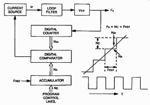
FIG. 66. Digital synthesizer using comparator and counter.
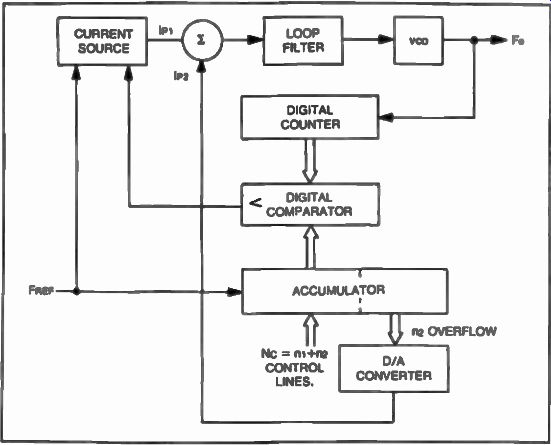
FIG. 67. The Digiphase approach.
A further improvement of the Digiphase method has been reported and is called the fractional-N synthesis. Although, this method resembles the Digiphase approach, it looks like a phase-locked synthesizer as shown in FIG. 68. Further improvements to the Digiphase method of synthesis has been introduced by Racal (patents pending). This consists of a further reduction of the low-frequency components at the output of the phase detector by using digital techniques. The output of the accumulator in FIG. 68 is further integrated in a similar size accumulator. When an overflow occurs from the second accumulator, a pulse is removed from NI . By adding this pulse to the next count, a greater phase is obtained for one reference period, balancing out the continuously decreasing phase due to (F. / NI ) > F REF . The Digiphase and the fractional N synthesizer are finding increased use in communication receivers today.
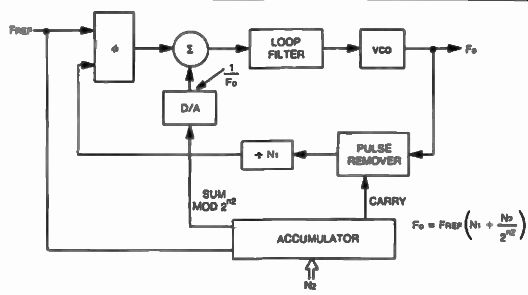
FIG. 68. Fractional N synthesizer block diagram.
SYNTHESIZER PITFALLS IN COMMUNICATIONS RECEIVERS
Because of the vast meaning of the word synthesizer, there are many misunderstandings about what a synthesized radio receiver should be. It is clear from the previous paragraphs that a synthesizer derives its stability from the reference oscillator whose stability has further impact on the receiver's performance circuitry. Unless all other frequency sources used in the receiver are also slaved to the same reference frequency, the receiver is considered as not fully synthesized. There are many receivers claiming frequency synthesis on the market today. While a phase-locked loop is usually used in the first conversion to provide large steps in resolution (usually 1 MHz), a variable-frequency-oscillator (Vfo) or some other form of free-running oscillator (permability tuned oscillator-PTO) is used to fine tune each range. The Vfo has a relatively unstable characteristic over the temperature range and tends to spoil the total frequency stability of the receiver.
Some receivers use vco's in the second or third conversions. Fine increments of dc voltage are provided through a D/A converter and a network of precision resistors to the vco's varactor. Although this method accepts digital commands which can be fed from the same thumb-wheel control switch that feeds the rough tuning synthesizer, the stability of the entire receiver depends on the temperature characteristic of the resistors used in the D/A converter. This method is not superior in frequency stability to a Vfo approach, because of its open loop nature. The design and development cost of a fully synthesized receiver, far exceeds that of a quasi-synthesized approach. One may ask why does anyone need a few Hz stability after all? In specialized radio communications, a radio receiver can be asked to do a variety of tasks, such as tune several ranges of frequencies in a particular manner selecting different bandwidths. It can also be programmed to be active at certain frequencies and/or time. Upon receiving a wanted signal, a second receiver can be activated to analyze that frequency, while the first receiver continues its predetermined task. The importance of being on the right frequency is vital, especially if narrow frequency shift-keying (FSK) is the mode to be received. If the receiver wasn't fully synthesized and inherently very stable, errors would result at the output of the FSK demodulator decreasing the probability of intercept in a system which is already affected by fading and noise phenomena.
*This frequency was chasten 35% higher than the highest frequency to be received of 500 MHz (a down converter is used for higher frequency coverage).
THE SR-2090 SYNTHESIZED COMMUNICATIONS RECEIVER
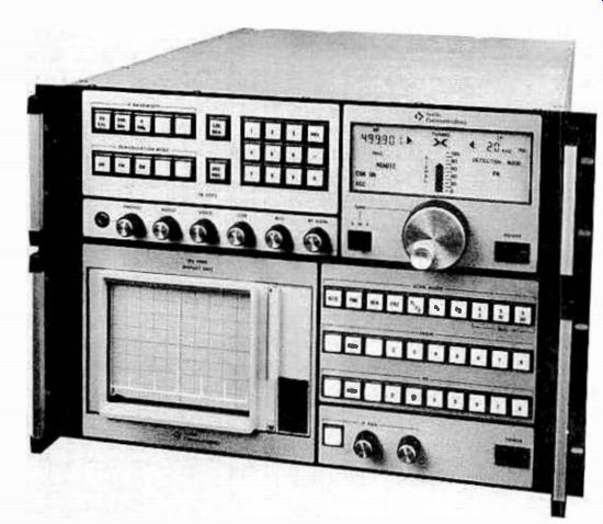
FIG. 69. The SR-2093 synthesized communications receiver shown with
the DM-2090 display unit (courtesy of Norlin Communications).
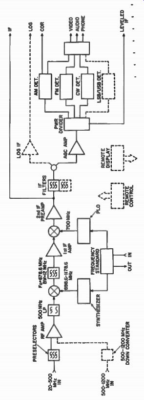
FIG. 70.
Table 3. Specifications of the SR-2090 Receiver.
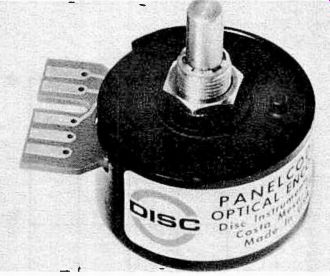
FIG. 71. An opto- encoder (courtesy of Disc Instruments).
Figure 69 shows the basic SR-2090, synthesized communications receiver, which is one of several configurations achieved with the SR-2000 series, manufactured by Norlin Communications. These receivers can provide full coverage from 0.5 MHz to 1200 MHz by using a synthesizer with a resolution of 10 Hz (standard resolution is 1 kHz). The basic system yields a double-conversion approach with the first i-f at 678.6 MHz*, and the second i-f at 21.4 MHz. Rf inputs from the antenna are filtered by one of several microprocessor-controlled, sub-octave pre selectors, which are designed in order to reject any second-order inter modulation products, followed by a broadband, low-noise amplifier with a very high IMD intercept point which in turn is inputted to the first mixer.
The mixer is of the high-LO-level doubly-balanced type in order to keep intermodulation distortion to a minimum.
The synthesizer operating between 698.6 MHz to 1178.6 MHz is fed to the LO port of the mixer, and the resultant i-f at 678.6 MHz is further filtered by a 12 MHz wide filter, and amplified in the first i-f amplifier which has just enough gain to overcome mixer loss while keeping the intermodulation distortion low.
This signal is further mixed with the 700 MHz phase-locked loop frequency which provides the fine resolution necessary for tuning. A converted 21.4 MHz signal at the second i-f is produced as a result, and filtered in the microprocessor-controlled filter bank, which provides receiver final selectivity. The microprocessor also controls the audio/video amplifiers, as well as the agc signal for the previous stages.
Since the receiver is entirely synthesized, it can be remotely con trolled by an external computer, or other digital commands, with the addition of an interface module. Several receivers can be remote control led, providing full master/slave capabilities, not only for the frequency control part, but for all functions involved including several memories for recalling preprogrammed, or microprocessor-calculated stations, for all functions involved including several memories for recalling preprogrammed, or microprocessor-calculated stations.
One human operator can control "hands-off" several slave receivers preprogrammed to do a variety of tasks at a variety of times, with computer precision, in an environment which might not allow for individual hand tuning of each receiver. This receiver is modular in packaging, allowing for full system flexibility in frequency coverage, with a minimum of electrical changes. Figure 70 shows the block diagram of the SR-2090 receiver and Table 3 lists the characteristics of this receiver.
THE OPTO-ENCODER AND ITS APPLICATION
In order to duplicate the tuning feel of the Vfo, the synthesized receiver uses a digital optical encoder. It has been seen that a synthesizer responds to computer-like encoded information to step from one frequency to another. To input this information, it is easiest to use a detented thumb-wheel encoder as we previously discussed. While such a method is fully adequate for some fixed applications, or for rough tuning, fine tuning a receiver with this method is rather impractical from an operator standpoint.
A knob-like dial which will provide a feel similar to the familiar old Vfo is desired. This function is achieved with the help of the opto-encoder. Figure 71 shows an opto-encoder manufactured by Disc Instruments.
The opto-encoder is usually a film or metal disc with holes in certain locations. An infrared beam shines through the holes. Two photocells detect when the light is interrupted, as well as the direction of rotation.
Information in the form of pulses is presented to a chain of up/down counters which are commanded to count in the direction of movement of the disc. This information is finally presented in a parallel format to the synthesizer's dividers, and an imitation Vfo feel is realized by the operator.
This process is illustrated in FIG. 72.
DESIGNING GOOD VFO'S
Let's return now briefly to the Vfo. Whether buying or designing a receiver, Vfo stability can be as important as dynamic range. Several years ago, many receivers had to be turned on at least one-half hour before operating to obtain adequate stability. Component warm-up especially in vacuum tubes, made excessive drift a fact of life even though these Vfo's were temperature-compensated with the use of NPO and NTC capacitors.
However, finding the right values and temperature coefficients for compensation was a long and tedious task. Today we need not worry about drift when using synthesizers. Modern Vfo's use FETs instead of tubes for better frequency stability. Polystyrene capacitors have proven to have extremely good stability characteristics, replacing the NPO and NTC capacitors.
Whenever designing a Vfo, such as the one shown in FIG. 1, remember one rule of thumb: several small polystyrene capacitors in parallel will provide much better stability than one large capacitor. Another rule is to buffer the Vfo and to use a good filter in the output in order to eliminate harmonics.
Bipolars should be avoided in Vfo's. Because of their typical low impedance levels, they demand a high L to C ratio, resulting in variable capacitors as high as 500 pF for inductances as little as 1 ,s2k1 in a 5 MHz Vfo, for example. A change of a fraction of a p.11 can cause severe drift in such a case, and this is entirely possible with inductors which rely on slug-tuned powdered iron or ferrite as core material. Perhaps one of the worst cores that can be used in this application is a toroid, because of the large area being exposed to temperature changes. Experience has shown that a ceramic form without any core is the best for winding Vfo coils on. increased stability is obtained by covering the finalized coil with paraffin or wax.
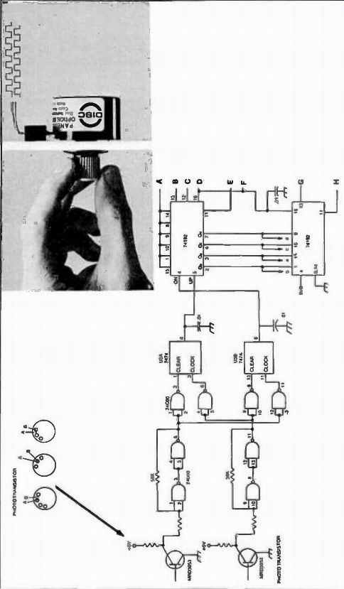
FIG. 72. An optical encoder is used in this example to provide fine
tuning for a communications receiver (courtesy of Disc Instruments).
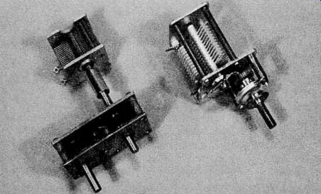
FIG. 73. Typical Vfo capacitors showing mechanical gears.
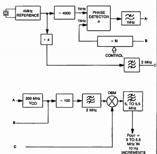
FIG. 74. Block diagram of a synthesized Vfo. Output is 5 to 5.5 MHz
in 10 Hz steps.
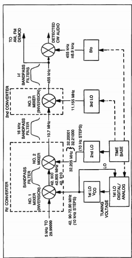
FIG. 75

Table 4. Specifications of the W1-8718 Receiver.
Table 5. Specifications of the R 4245 Receiver.
There is no substitute for a quality variable capacitor (FIG. 73). The use of capacitors with aluminum plates should be avoided. They can be noisy and microphonic. It has been found that the smoothness of the plates in a variable capacitor had a significant effect on the Q and the noise floor of a Vfo. A mirror-like surface would be preferred. Finally, the mechanics should not be ignored. Springy couplers if they are used can introduce backlash. Noise in Vfo's and phase noise in synthesizers can account for a lot of intermodulation products which will participate in the receiver's dynamic range, making it sound "mushy" and lowering the effective intercept point. Much has been written on Vfo's but the one shown in FIG. 1 is a good example of a clean and stable modern design.
It is possible to build a digital Vfo by using the phase-locked loop techniques described earlier. Figurel5 -74 shows the block diagram for a 5 to 5.5 MHz system. The vco operates at 200 MHz in order to allow for a relatively high reference frequency of 1 kHz, which in turn provides fast switching for a final resolution of 10 Hz at the output of the synthesizer.
This approach could be used with any of the presently manufactured transceivers requiring a 5 to 5.5 MHz Vfo, however, this modification will not transform the rig into a truly synthesized apparatus because of the requirement for additional mixing with crystal oscillators which are internal to the transceivers. Unless these sources are also slaved to the same reference frequency as the Vfo synthesizer, the system is said to be a quasi-synthesizer approach.
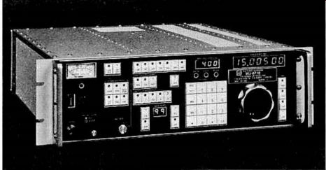
FIG. 76. The Watkins-Johnson WJ-8718 is a highly versatile, fully
synthesized (including the bfo) hf receiver which covers the frequency
range of 5 kHz to 30 MHz in one band, with a resolution of 10 Hz and
a typical lock-up time of 3 ms (courtesy of Watkins-Johnson Company).
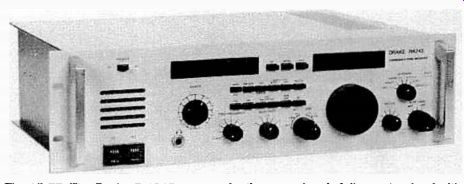
FIG. 77. The Drake R 4245 communications receiver is fully synthesized
with a shaft encoder replacing the variable tuning oscillator and allowing
for variable rate tuning (2 kHz per revolution if turned slow, and 20
kHz per revolution if the speed of tuning Is Increased). The receiver
has a spurious free dynamic range (SFDR) of 99 dB (Two tone test spaced
100 kHz apart). (courtesy of R.L. Drake Co.).
In conclusion, we discussed several ways of implementing local oscillators in communications receivers, with the accent on several forms of synthesizers which can allow for all local oscillators in a radio receiver to be coherent with a highly stable reference frequency. Figure 75 shows the block diagram of the WJ-8718 high frequency communications receiver, manufactured by Watkins-Johnson. It can be seen from this example that all local oscillators in this triple-conversion approach are slaved to the time base generator. Also, see Figs. 76, 77 and Tables 4 and 5.
Although several books alone can be written on the subject of synthesized local oscillators, this Section was intended as a triggering mechanism for those interested in furthering the cause of technical excellence.