CIRCUIT NO. 1--POWER SUPPLIES
Of the four power supplies shown, two provide fixed voltages and two continuously variable voltages within their rated values. In the fixed-voltage supplies, Circuits No. 1 (a) and No. 1 (b), the output voltage can be adjusted to a set value by replacement of certain circuit components with other components of different value. The universal series power supply, Circuit No.1 (a), is designed for use with electrical circuits requiring at least 6 volts but less than 35 volts. The universal shunt power supply, Circuit No. 1 (b), is most suitable for applications requiring 6 volts or less.
The exact dc output voltage of a fixed supply is dependent on the regulator circuit, on the transformer used in the transformer-rectifier stage, and on the configuration of that stage. Fig. 51 shows the two transformer-rectifier output voltages and the regulator circuit (series or shunt) and transformer rectifier stage to be used to produce each output voltage.
-----------------------
Parts List
C1 = capacitor, electrolytic, see Table IV for value
CR1 CR 2 CR3 CR4 = silicon rectifier, RCA SK3030
F1 = fuse, 1 ampere
S1 = switch, 125 volts, single-pole, single-throw
T1 = transformer, primary 120 volts, secondary current rating 1 ampere, see Table IV for voltage.
If the secondary voltage in Table IV is 6.3 use Stancor No. P-8190 or equivalent; if voltage is 12.6 use Stancor No. P-8130 or equivalent: For all other voltages use Stancor No. TP-4 or equivalent.
--------
--------
Fig. 51 - Transformer-rectifier stages used with the fixed power supplies.
---------
Fig. 52(a)- Fixed power supply.
-----------
Table IV. Fixed Power Supply Design Chart Transformer-Rectifier Stage Regulator
Circuit
---------------
... stages; Table IV shows the possible dc
In Fig. 5 1(a), transformer T1 isolates and steps down the line voltage, which is then full-wave rectified by diodes CR1 and CR2 and filtered by capacitor C1 . When the circuit shown in Fig. 5 1(b) is used, the series or shunt circuit receives full-wave rectified ac from a bridge rectifier rather than from a two-diode center-tapped trans former secondary. The bridge rectifier arrangement provides the regulator with a high input voltage. Fig 52 (a) shows a fixed supply.
In the variable-voltage supplies, the output voltage can be varied during operation by means of a potentiometer control. The limited-range variable supply, Circuit No.1 (c), delivers from about 4.5 to 12 volts.
The full-range
The universal series power supply is a fixed voltage supply that performs best with circuits requiring at least 6 volts and any intermediate value up to a maximum of 35 volts.
The schematic diagram and parts list for the universal series power sup ply are shown in Fig. 53. The full-wave rectified voltage received from the transformer-rectifier combination of Fig. 51 is applied across the regulator circuit consisting of transistors Q1 and Q2 and zener diode CR1. The purpose of the regulator circuit is to maintain a constant voltage across the load; with out this circuit an increased load would variable supply, Circuit No.1 (d), delivers any voltage between zero and 12 volts. Fig. 52 (b) is a photograph of a variable supply.
The power supplies are suitable for use with the circuits in this Manual and for many other applications. The specific supply used is determined by the power requirements of the intended application. The maximum output current of any of these supplies is 1 ampere.
Fig. 52( b)- Variable power supply.
Circuit No. 1 (a) - Universal Series Power Supply
------------
b. Parts List
C1 = 100 microfarads, electrolytic, see text
C2 = 0.1 microfarad, 50 volts or greater
CR 1 = zener diode, 1 watt, see Table IV for voltage
Q1 = transistor, RCA SK3027
Q2 = transistor, RCA SK3020
R1 = resistor, 1/2 watt, 10%, see Table IV for value
R2=220 ohms, 1/2 watt, 10%
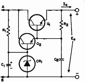
Fig. 53 - Schematic diagram and parts list for the universal series power
supply.
------------
... result in decreased load voltage. The operation of the regulator can best be understood by assuming that a constant voltage exists across the zener diode and the base-emitter junctions of Q1 and Q2 under all load conditions.
When a decrease in load voltage occurs, through an increase in load current or a decrease in line voltage, the base of transistor Q2 becomes more positive than its emitter and more base current flows. The increase in base current in Q2 increases the collector-to emitter current which, when applied to the base of transistor Q1 , reduces its collector-to-emitter voltage. This action on the part of Q1 maintains load voltage constant.
When the load voltage increases, through a decrease in load current or an increase in line voltage, an effect opposite to that described above takes place. The base current of transistor Q2 decreases, resulting in a decrease in its collector-to-emitter current. This collector-to-emitter current is applied to the base of Q1 and raises its collector-to-emitter voltage, again satisfying the conditions for constant load voltage.
In actual circuit operation, the voltage across the zener diode and the emitter-base junctions of Q1 and Q: changes slightly with a change in load current. However, because the polarity of the drop across the zener diode is opposite to the drop across the junctions, the effects of each tend to cancel.
The zener-diode and transformer secondary voltage ratings and the value of resistor R1 in Fig. 53 depend on the required amounts of load voltage E. and load current I_0. Table IV shows these values and ratings as a function of output voltage. The voltage rating of C1 should be higher but as close as possible to the voltage rating of CR1.
Circuit No. 1 (b) - Universal Shunt Power Supply
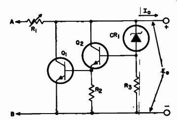
The universal shunt power supply is a fixed power supply designed to perform best when providing 6 volts or less.
The schematic diagram and parts list for the universal shunt power supply are shown in Fig. 54. The principles of operation of the shunt supply are similar to those of the series supply except that a resistor R1 rather than a transistor is used as the voltage-dropping element. The output voltage is held constant by Q1 , which regulates the current through, and therefore the voltage drop across, R1.
-------------
Parts List
CR1 = zener diode, 1 watt, see Table
R1 = adjustable, 5 ohms, 5 watts IV for voltage
R2 = 180 ohms, 1/2 watt, 10%
Q1 = transistor, RCA SK3027
R3 = 470 ohms, 1/2 watt, 10%
Q2 = transistor, RCA SK3020
------ Fig. 54 - Schematic diagram and parts list for the universal shunt
power supply.
------- As in the universal series power supply, load voltage is maintained constant by a regulator circuit composed of a zener diode in series with the base-emitter junctions of transistors Q1 and Q2 . As load current increases, the base current of transistor Q2 decreases and reduces the collector-to-emitter current flowing to the base of transistor Q1. This action reduces the collector current of Q1 so that less current flows through resistor R1 . When load current decreases, the regulator circuit increases the flow of current through resistor R1 and thus maintains a constant load voltage condition.
The zener-diode and transformer secondary voltage ratings and the values of resistor R1 and capacitor C1 in Fig. 54 depend on the required amounts of load voltage and load current. Table IV shows these ratings and values as a function of output voltage.
R1 should be adjusted so that it passes a current of 1.15 amperes; an ammeter is required for this adjustment.
Circuit No. 1 (c)- Limited-Range Variable-Voltage Power Supply
The limited-range variable-voltage power supply is a continuously adjustable supply capable of delivering from about 4.5 volts to 12 volts at a maximum current of 1 ampere.
The schematic diagram and parts list for the limited-range variable-voltage power supply are shown in Fig. 55.
The voltage-regulating circuit in this supply uses a transistor Q3 in conjunction with a zener diode. The base of Q3 is connected to the voltage-control resistor R4 , which, along with trimmer controls R3 and R5 , is in parallel with the load. Therefore, any change in load or output voltage affects the voltage at the base of transistor Q. If the output voltage tends to increase, the base of Q3 becomes more positive and more collector current flows. The increased collector current makes the base of Q2 less positive and reduces the collector to-emitter current supplied to the base of transistor Q1. Reduced base current in Q1 results in an increased collector to-emitter voltage drop in Q1 ; this voltage drop maintains load voltage at the desired level. The opposite effect occurs when the load voltage tends to decrease.
Resistors R3 and R5 are used to set the upper and lower voltage limits of the supply; these values normally need be set only once. Screw-driver-adjust trimmer-type potentiometers are the best types for R3 and R5.
------------
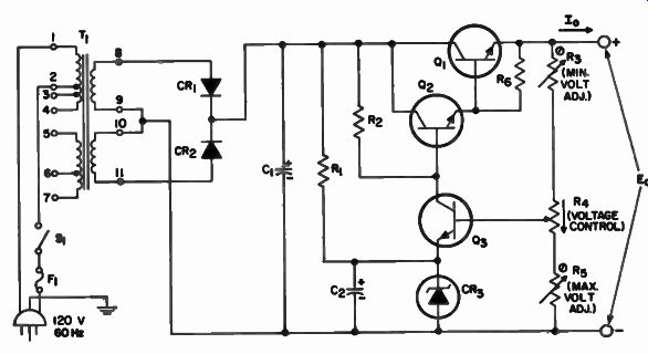
Fig. 55 - Schematic diagram and parts list for the limited-range variable-voltage
power supply
Parts List
C1 = 5000 microfarads, 25 volts, electrolytic
C2 = 100 microfarads, 6 volts, electrolytic
CR1 •CR2 = silicon rectifier, RCA SK3030
CR 2 = zener diode, 3.9 volts, 1/2 watt
F1 = fuse, 1 ampere, 120 volts
Q1 = transistor, RCA SK3027
Q2 Q3 = transistor, RCA SK3020
R1 = 6800 ohms, 1/2 watt, 10%
R2 = 10,000 ohms, 1 watt, 10%
R3 R5 = trimmer potentiometer, 5000 ohms, Mallory MTC-1 or equivalent
R4 potentiometer, 5000 ohms, linear taper
S1 = switch, 120 volts, 1 ampere, single-pole, single-throw
T1 = transformer, primary 115 volts, secondary 15 volts, 1 ampere, Stancor No. TP-4 or equivalent
-----------------
Circuit No. 1 (d) -Full-Range Variable-Voltage Power Supply
The full-range variable-voltage power supply is a continuously variable supply capable of delivering up to 12 volts at a maximum current of 1 ampere.
The schematic diagram and parts list for the full-range variable-voltage power supply are shown in Fig. 56. The regulator circuit in this supply receives full-wave rectified ac from a bridge rectifier rather than from a two-diode center-tapped transformer secondary as in the other power supplies described. This arrangement provides the regulator with a high input voltage.
This supply also differs from the others described in that it contains an additional zener diode, CR6 , connected in opposition to zener diode CR1. The transistors in the regulator circuit operate in the same manner as those in the other supplies, but handle twice as much voltage. This voltage does not appear across the load, however, because of CR 6. The voltage across CR6 is that across the center taps of the transformer and rectifying diodes CR1 and CR2. The load voltage is equal to the regulator voltage minus the voltage across zener diode CR6 . When the two voltages are equal, the load voltage is zero. If the regulator-circuit voltage falls below 12 volts, the base-emitter junction of transistor Q3 becomes reverse-biased and the transistor turns off. As a result, Q2 and Q1 also turn off and prevent the load voltage from reversing polarity (becoming negative).
Power-Supply Operation
The power supplies described are self-regulating after the desired output conditions are set through the use of an ammeter and voltmeter. In some applications, it may be desirable to have the ammeter and voltmeter connected as an integral part of the power supply so that output conditions can be monitored.
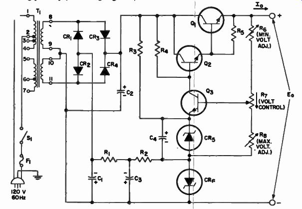
Fig. 56 - Schematic diagram and parts list for the full-range variable-voltage
power supply.
--------------
Parts List
C1 C3 = 500 microfarads, 25 volts, electrolytic
Cg = 5000 microfarads, 25 volts, electrolytic
C4 = 100 microfarads, 10 volts, electrolytic
CR1 CR2 CR3 CR4 = silicon rectifier, RCA SK3030
CR5 - zener diode, 6.8 volts, 1 watt
CR6 = zener diode, 12 volts, 1 watt
F1 = fuse, 1 ampere, 120 volts
Q1 = transistor, RCA SK3027
Q2 Q3 = transistor, RCA SK3020
R1 R5 = 220 ohms, 1/2 watt, 10%
R2 = 470 ohms, 1/2 watt, 10%
R3 = 6800 ohms, 1/2 watt, 10%
R4 = 10,000 ohms, 1/2 watt, 10%
R3 Re = trimmer potentiometer, 5000 ohms, Mallory MTC-1 or equivalent
R7 = potentiometer, 5000 ohms, linear taper
S1 = switch. 120 volts, 1 ampere, single-pole, single-throw
T1 = transformer, primary 115 volts, secondary 15 volts, 1 ampere, Stancor No. TP-4 or equivalent
--------------
Construction
For best performance, the supplies should be well ventilated. Transistor Q1 should be mounted on a heat sink if its maximum power dissipation (determined by multiplying collector current by collector-to-emitter voltage) is expected to exceed 6 watts. Heat sinks are discussed in the section on Mechanical Considerations. Maximum power dissipation occurs when the supply is set for minimum output voltage at an output current of 1 ampere.
All power supply transformers should have a dc resistance of at least 1 ohm. If the transformer used has a dc resistance of less than 1 ohm, a 1-ohm, 2-watt resistor should be inserted in series with the secondary. If a center tapped supply is used, the resistance should be placed in series with the center tap. No special precautions are required if the transformers specified in the parts list are used.
CIRCUIT NO. 2 - SHIFT REGISTER
In a shift register, the successive outputs from the various stages are delayed (or shifted) from those of the preceding stages by a controlled time interval (i.e., the duration between input trigger pulses). These outputs can be used to operate lamps (as shown in Circuits No. 23 and No. 24) or can be coupled through OR gates to establish a timing sequence for various operations of other equipment. If terminal 15 of the circuit (Fig. 57) is connected to terminal 16, the register becomes regenerative and can be used as a ring counter. In a ring counter, each stage follows in sequence as if placed around a circle or ring. Each pulse input to the ring advances the counter one stage; when the last stage is reached, the next pulse activates the first stage. The cycle repeats until input pulses are stopped.
The shift register may incorporate as many stages as desired.
Circuit Operation
The schematic diagram and parts list for a 10-stage shift register are shown in Fig. 57. The 10.6-volt dc supply voltage is obtained from two diodes connected in series as shown in Fig. 57. With these voltages applied, switching transistor Q1 is immediately turned on by the positive voltage applied to its base through Ra. One of the register stages must be triggered simultaneously to provide a complete path for the current through the switching transistor.
Each register stage is basically a two-transistor regenerative switch that employs an n-p-n and a p-n-p transistor. If either of the transistors in a register stage starts to conduct, both of them are quickly driven into saturation by the regenerative action of that stage.
------------
Parts List
C1 = 100 microfarads, 10 volts, electrolytic
C2 C4 C5 CN 0.05 microfarad, 50 volts or greater
C3 10 microfarads, 15 volts, electrolytic
CR 1 CR2 CRN = silicon diode, type 1N270
Q1 Q3 Q5 QN'= transistor, RCA SK3005
Q2Q4QN = transistor, RCA SK3010 R1 R7 RN = 1000 ohms, 1/2 watt, 10% R2 = 47 ohms, 1/2 watt, 10% R3 = 5600 ohms, 1/2 watt, 10% R4R5 = 470 ohms, 1/2 watt, 10% Rs Rs R /I= 270 ohms, 1/2 watt, 10%
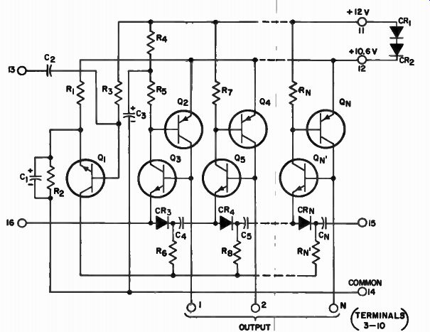
------ Fig. 57 - Schematic diagram and parts list for the shift register.
------
When power is applied to the shift register circuit, capacitor C3 starts to charge. The charging action provides Q2 with a base current and turns it on.
Q2 then turns Q3 on. The stage composed of Q2 and Q3 is then in conduction and provides an output at terminal 1. Q3conducts through Q1. The voltage across R8 charges C4 through CR2 and Re. The circuit remains in this state until an input trigger pulse is applied.
To shift the register to the next stage, a negative pulse of 2 volts or more is applied to the base of Q1 through C2. This pulse turns off Q2 momentarily, interrupts the emitter circuit of Qa , and turns that stage off.
When Q1 is off, all stages are nonconducting. When Q1 returns to its con ducting state, the first stage does not turn on because C3 is fully charged; however, the charge on C4 places a forward bias on the emitter of Q5and it turns on. Q4 is then turned on and produces an output. When Q4 is in conduction, C5 charges and ensures that the third stage will trigger with the next input pulse. In this way, the operation of the register is shifted from one stage to the next each time a negative trigger pulse is applied. By interrupting the power and allowing C3 to discharge, the register can be reset so that operation starts with the first stage.
It is important that the load connected to the outputs (1, 2, N) be 1000 ohms or less. The load current should not exceed 200 milliamperes.
Construction
Figs. 58
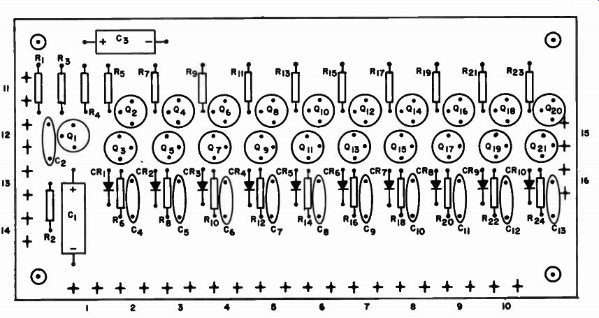
The drilling template for a 10-stage shift register is shown at the back of this Manual; a component placement diagram and a photograph of the completed circuit board are shown in Figs. 58 and 59, respectively.
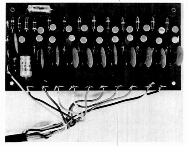
Fig. 59 - Completed circuit board for a ten-stage shift-register.
CIRCUIT NO. 3 - SIMPLE CODE-PRACTICE OSCILLATOR
The simple integrated-circuit (IC) code-practice oscillator is an excellent project for the beginning radio amateur. Construction provides exposure to the use of integrated circuits and practical knowledge of circuit-building techniques; the finished oscillator is a valuable tool for learning the Morse code.
Circuit Operation
The schematic diagram and parts list for the code-practice oscillator are shown in Fig. 60. The heart of the oscillator is the integrated circuit, CA3028. The schematic diagram for the integrated circuit is shown in Fig. 61; all components shown in this dia gram are within the integrated-circuit package. Transistors Q1 and Q2 of the integrated circuit comprise a differential amplifier which is driven by a constant-current source Q. The feedback necessary for oscillation is supplied to Q1 through external capacitor C1. The remainder of the resistors both internal and external to the integrated circuit provide proper voltage bias conditions.
The current drain for this circuit is approximately 5.5 milliamperes.
Construction
The drilling template for the code practice oscillator is shown at the back of this Manual; a component placement diagram and a photograph of the completed circuit board are shown in Figs. 62 and 63, respectively.
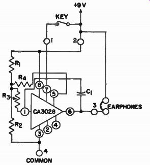
Fig. 60 - Schematic diagram and parts list for the simple code-practice oscillator.
Parts List
= 0.47 microfarad, 25 volts or greater, 10%
R1 R3 R4 = 1000 ohms, 1/2 watt, 10%
R2 = 2000 ohms, 1/2 watt, 10%
Integrated Circuit = RCA CA3028
Earphones = 2000 ohms, magnetic
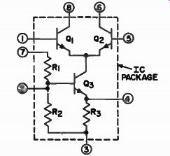
Fig. 61 - Schematic diagram of the CA3028 integrated circuit (all components
shown are inside the integrated-circuit package).
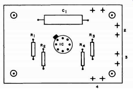
Fig. 62 - Component placement diagram for the simple code-practice oscillator.
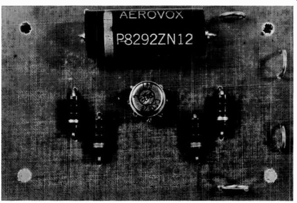
Fig. 63 - Completed circuit board for the simple code-practice oscillator.
CIRCUIT NO. 4 -- AUDIO OSCILLATOR
The audio oscillator has been designed for code practice; an optional output that can be used to key a relay is provided. The oscillator output ton( is a sine wave.
Circuit Operation
The schematic diagram and parts list for the audio oscillator are shown in Fig. 64. Transistor Q1 , capacitors C1 , C2 , C3 , and C4 , and resistors R1, R2 , and R3 form a basic twin-T oscillator (as described in the section on General Circuit Considerations). Briefly, transistor Q1 is a standard audio amplifier; its collector is connected to the twin-T network composed of C1 , C2 , and C3 , and R1, R2, and R3. The output of this network is applied to the base of transistor Q through capacitor C4 and supplies the required feedback for oscillation. The output of Q1 is applied to Q3 , which is connected into the circuit in a common-emitter configuration (as discussed in the section on Theory and Operation of Solid-State Devices). Qs provides a power gain and the ear phone output signal. Potentiometer R1, sets the audio level in the ear phones.
When the circuit is used to key a relay, the hand key is connected through R8 to the base of Q2; power input should be 12 volts. Transistor Q2 switches power to Q1 as well as to the relay. Diode CR, protects Q2 from the high inductive voltages that are present at the terminals of a relay when the relay-coil circuit is interrupted.
When the circuit is used as a code practice oscillator and a relay is not required, Q2, CR,, R8, and R9 are omitted, A and B are disconnected,
Circuits
and the wiring shown by dashed lines in Fig. 64 is substituted.
In the idle state, the current drain for this circuit is approximately 200 microamperes; when keyed, the drain is 7.5 milliamperes.
Construction
The drilling template for the audio oscillator is shown at the back of this Manual; a component placement dia gram and a photograph of the completed circuit board are shown in Figs. 65 and 66, respectively.
----------
Parts List
C1 C2 = 0.0047 microfarad
C3 C4 = 0.01 microfarad
C. = 1 microfarad, 6 volts, electrolytic
Ce = 5 microfarads, 6 volts, electrolytic
CR1 = silicon rectifier, RCA SK3030
Q1 Q3 = transistor, RCA SK3020
Q2 = transistor, RCA SK3005
R7 = 10,000 ohms, 1/2 watt, 10%
R2 R3 = 47,000 ohms, 1/2 watt, 10%
R4 = 100,000 ohms, 1/2 watt, 10%
Rs - 22,000 ohms, 1/2 watt, 10%
Rs = 6800 ohms, 1/2 watt, 10%
R7 = 2200 ohms, 1/2 watt, 10%
R9 = 12,000 ohms, 1/2 watt, 10%
R. = 470 ohms, 1/2 watt, 10%
R10 = 820 ohms, 1/2 watt, 10%
R77 = potentiometer, 5000 ohms, linear taper
Earphones = 600 ohms or greater
Relay = 12 volts, 1350 ohms, Potter and Brumfield No. RS5D or equivalent
S1 = telegraph key or switch
-------------------
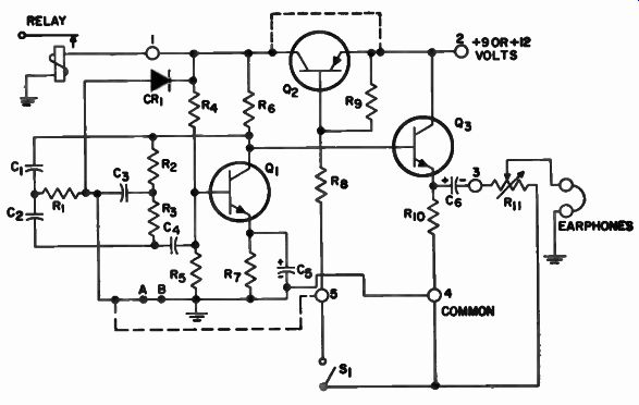
Fig. 64 - Schematic diagram and parts list for the audio oscillator.
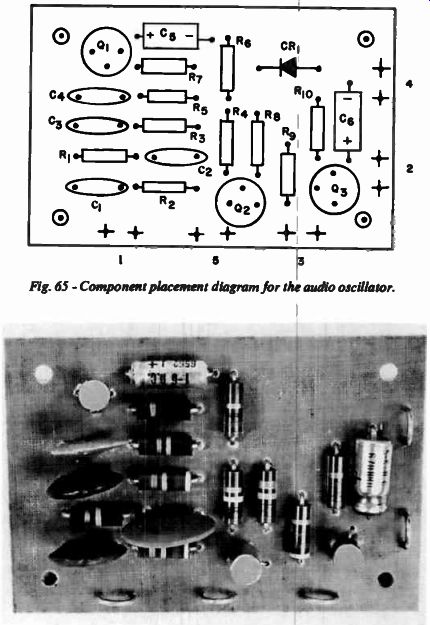
Fig. 65 - Component placement diagram for the audio oscillator.
Fig. 66 - Completed circuit board for the audio oscillator.
CIRCUIT NO. 5 - SEMI-AUTOMATIC ELECTRONIC KEYER
--------------
Parts List
C1 = 5 microfarads, 25 volts, electrolytic
C2C 2 = 560 picofarads, 50 volts or greater = 330 picofarads, 50 volts or greater CR1 CR4 Cits
CR6 = silicon rectifier, RCA SK3030
CR2 CR2 = silicon rectifier, type 1N270
Q1 Q3 Q7 = transistor, RCA SK3005
Q2 Q Q5 Q6 = transistor, RCA S K3020
R1 = 1000 ohms, 1/2 watt, 10%
R2 = 180 ohms, 1/2 watt, 10%
Rs R17 R19 = 2200 ohms, 1/2 watt, 10%
C C5 R. = 2700 ohms, 1/2 watt, 10%
R5 R18 = 470 ohms, 1/2 watt, 10%
R3 = 1500 ohms, 1/2 watt, 10%
R7 = 39,000 ohms, 1/2 watt, 10%
Rs R1. = 3900 ohms, 1/2 watt, 10%
Rs R15 = 15,000 ohms, 1/2 watt, 10%
Rio R12 = 33,000 ohms, 1/2 watt, 10%
R13 = 27,000 ohms, 1/2 watt, 10% 12,000 ohms, 1/2 watt, 10% potentiometer, 10,000 ohms, linear taper
Relay = 12 volts, 1350 ohms, Potter and Brumfield No. RS5D or equivalent
R11 R16 = R2o =
--- Fig. 67- Schematic diagram and parts list for the semiautomatic electronic
keyer.
-----------
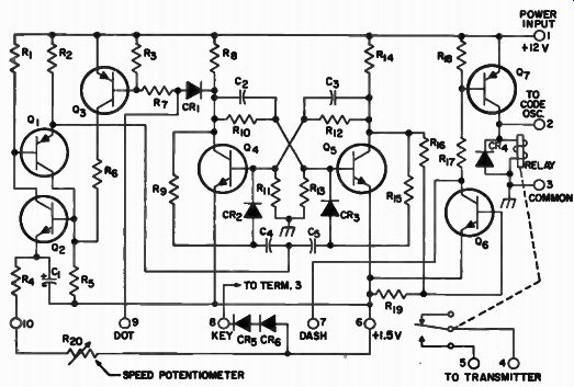
The semiautomatic electronic
Morse-code keyer or "bug" generates a single dot or a series of dots, depending upon how long the paddle-key is depressed; the dash must be made manually. The rate at which dots are generated can be varied.
Circuit Operation
The schematic diagram and parts list for the semiautomatic keyer are shown in Fig. 67. The dot repetition rate is determined by R4, C1, and the speed potentiometer R20. These components control the regenerative switch consisting of transistors Q1 and Q2.
This switch has a very high impedance before it is triggered and a very low impedance afterward. When the paddle-key is moved to the dot position, the current applied to the base of Q3 turns it on and permits C1 to begin charging through the emitter of Q2. At the same time, Q2 turns on and triggers the regenerative switch into conduction. As capacitor C1 charges, the emitter of Q2 becomes more and more positive until the regenerative switch is cut off. When cutoff occurs, the impedance of the regenerative switch becomes very high and C1 is forced to discharge through R4 and the speed potentiometer R20. As the charge on C1 decreases, the emitter of Q2 becomes less positive and the regenerative switch begins to conduct again. This process repeats itself as long as the paddle-key is held in the dot position.
The polarity of the regenerative switch in conduction is such that a negative pulse is applied to the base of transistors Q4 and Q6 in the flip-flop. This negative pulse is sufficient to turn on transistor Q4 Q5 turns off automatically as a result of normal flip-flop action. When Q5 is off, its collector voltage is applied to Q6 through R15, and Q6 turns on. Current through Q6 activates Q, which, in turn, closes the output relay. Diode CR4 is placed across the relay to protect Q7 from the high-voltage inductive discharges which occur when current to the relay coil is interrupted and its coil field collapses.
When the paddle-key is released from the dot position with Q4 off (i.e., when the paddle-key is released at the end of a dot), Q3 turns off and interrupts the C1 charging path, with the result that the regenerative-switch pulses that cause the dots are stopped.
When the paddle-key is released from the dot position with Q4 on (i.e., when the paddle-key is released in the middle of a dot), Q3 continues to conduct because its base current continues to flow through 04. The regenerative switch pulses once more to complete the dot cycle. Dot-cycle completion is accomplished when the final regenerative-switch pulse returns the flip-flop to its original state and turns Q4, and consequently Q3, off.
If instead of batteries a power sup ply is used to power this circuit, the 1.5 volts needed (shown as an input at circuit-board terminal No. 6) can be obtained from the drop across the two silicon rectifiers CR5 and CR6 connected in series, as shown in Fig. 67.
When the paddle-key is in the dash position, the relay is not under the control of a transistor, but operates directly.
The current drain for this circuit is approximately 5 milliamperes.
Construction
The semiautomatic electronic keyer is built on the same circuit board as the automatic keyer, Circuit No. 6. The drilling template for both circuits is shown at the back of this Manual; a component placement diagram is shown in Fig. 70.
CIRCUIT NO. 6 - AUTOMATIC KEYER
This fully automatic keyer produces either dots or dashes continuously for as long as the paddle-key is held in the dot or dash position. The speed of the dots and dashes can be varied to suit the operator. The keyer circuit is composed of a number of the building blocks described in the section on General Circuit Considerations: the pulser or clock, the flip-flop, and the lamp driver. The 12-volt supply is needed to power the keyer; eight flash light batteries in series or a 12-volt supply such as that described in Circuit No. 1(a) may be used.
Circuit Operation
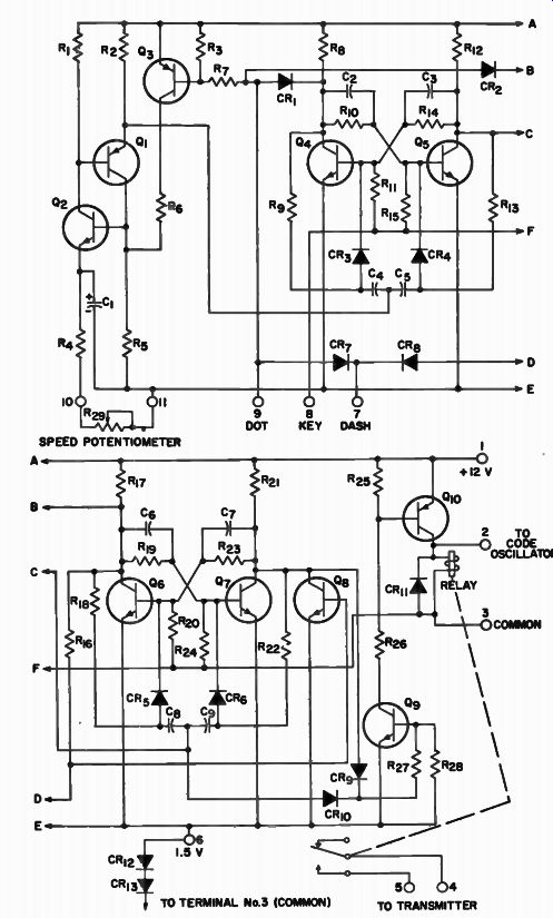
Fig. 68 - Schematic diagram for the automatic keyer.
Parts list on next page.
----------------
Parts List
C1 - 5 microfarads, 25 volts, electrolytic
C2C2C6C7= 560 picofarads, 25 volts or greater
C4 Cs Cg C9 = 330 picofarads, 25 volts or greater
C R1 through CR io = silicon rectifier, type 1N270 CRIICRI2CRI3= silicon rectifier, RCA SK3030 Q1Q3Q19 = transistor, RCA SK3005 Q2Q4Q5 through Q9 = transistor, RCA SK3020 R1 = 1000 ohms, 1/2 watt, 10% R2 = 180 ohms, 1/2 watt, 10% R3 R26 R28 = 2200 ohms, 1/2 watt, 10% R4 = 2700 ohms, 1/2 watt, 10% R5 R25 = 470 ohms, 1/2 watt, 10% R6 = 1500 ohms, 1/2 watt, 10% R7 R16 = 39,000 ohms, 1/2 watt, 10% R9 R12 R17 R21 = 3900 ohms, 1/2 watt, 10% R9 R1312.19 R22 = 15,000 ohms, 1/2 watt, 10% R10 R14 R19 R23 = 33,000 ohms, 1/2 watt, 10% R11 R15 R20 R24 = 27,000 ohms, 1/2 watt, 10% R27 = 12,000 ohms, 1/2 watt, 10% R29 = potentiometer, 10,000 ohms, linear taper
Relay = 12 volts, 1350 ohms, Potter and Brumfield No. RS5D or equivalent
---------------------
The schematic diagram and parts list for the fully automatic keyer are shown in Fig. 68. The dot or dash repetition rate of the keyer is determined by speed-control potentiometer R29, which controls the frequency of the pulser or clock oscillator consisting of transistors Q1 and Q. When the paddle-key is moved to the dot position (i.e., when terminals 8 and 9 on the circuit board are connected), a current is transmitted to the base of Qa ; this current turns Q3 on. Q3 in turn activates the regenerative switch consisting of Q1 and Q2 and permits C1 to begin charging through the emitter of Q2. As capacitor C1 charges, the emitter of Q2 becomes more and more positive until Q2 is cut off. When cutoff occurs, the total impedance of Q1 and Q2 becomes very high and C1 is forced to discharge through R4 and the speed control potentiometer R29. As the charge on C1 decreases, the emitter of Q2 becomes less positive and transistors Q1 and Q2 begin to conduct again.
This process repeats itself as long as the paddle-key is held in the dot or dash position. Q1 and Q2 when in conduction produce a negative pulse that is applied to the bases of transistors Q4 and Q5 in the flip-flop. This negative pulse is sufficient to turn off transistor Q5 ; Q4 is turned on automatically as a result of normal flip-flop action. When Q5 is off, current is conducted through R12, CR 10, and R27; this current turns Q6 on. Current through Q6 activates Q1, which, in turn, energizes the output relay.
The dash flip-flop composed of transistors Q6 and Q7 is held inoperative during the dot cycle by the clamping transistor Q6 which is held in the conductive state by current through R17 and R16. Diode CR11 is placed across the relay to protect Qi0 from the high-voltage pulse produced when current to the relay is interrupted and its coil field collapses.
When the paddle-key is released from the dot position with Q4 off (i.e., when the paddle-key is released during a space at the end of a dot or a series of dots), Q 3turns off and the oscillator pulses that cause the dots are no longer generated. When the paddle-key is released from the dot position with Q4 on (i.e., when the paddle-key is released in the middle of a dot), Q3 continues to conduct and permits the oscillator pulse to complete the dot cycle. This last pulse turns Q4, and consequently Q3 , off, and the oscillator pulses cease.
A dash or series of dashes is produced when terminals 7 and 8 are connected (i.e., wEen the paddle-key" is moved to the dash position). Under this condition Q3 is turned on by a signal applied to its base through R7 and CR7. At the same time Q8 is turned off by the grounding of its base through CR8 . The first pulse from the clock oscillator sets both the dot and dash flip-flops to the output state. Q3 receives a base signal not only from the paddle-key but from the dash flip-flop through CR2 and the dot flip-flop through CR1. Q9 receives a dash signal from either the dash or dot flip-flop through their respective diodes CR9 or CR10. The second pulse from the oscillator sets the dot flip-flop to the no output state but does not disturb the dash flip-flop, and Q9 remains in the conducting state. The third pulse sets the dot flip-flop to the output state and the dash flip-flop to the no-output state, and Q9 remains conductive.
When a fourth pulse is developed, both flip-flops are in the no-output state and Q9 is turned off. If at this time the paddle-key is in the neutral or middle position (circuit-board terminals 7 and 8 disconnected), Q3 is also turned off and the system returns to its quiescent state. If the key is still in the dash position, the cycle repeats. Fig. 69 shows the voltage and current wave forms at selected points in the circuit. Relay current during a single dash cycle flows for a time equal to three dots and is cut off for a period equal to one dot.
The current drain for this circuit is approximately 20 milliamperes.
Special Considerations
If instead of batteries a power sup ply is used to power this circuit, the 1.5 volts needed (shown as an input at circuit-board terminal No. 6) can be obtained from the drop across the two silicon rectifiers CR12 and CR13 connected in series, as shown in Fig. 68.
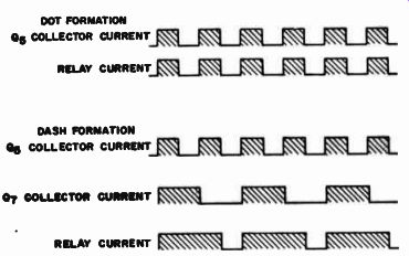
Fig. 69 - Voltage and current waveforms at selected points in the automatic
keyer circuit.
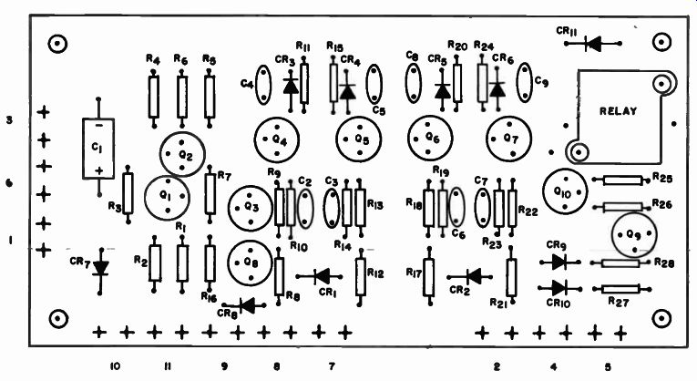
Fig. 70 - Component placement diagram for the automatic keyer.
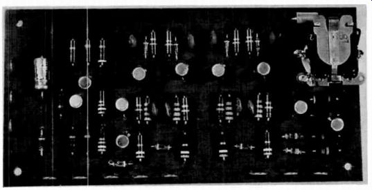
Fig. 71 - Completed circuit board for the automatic keyer.
Construction
The drilling template for the automatic keyer is shown at the back of this Manual. A component placement diagram and a photograph of the completed circuit board are shown in Figs. 70 and 71, respectively.
CIRCUIT NO. 7 MICROPHONE PREAMPLIFIER
The microphone preamplifier is capable of boosting the output of a dynamic microphone to a 0.5- to 1-volt level. This level is compatible with the mixer, volume compressor, and line amplifier (Circuit No. 8) and the audio power amplifier circuit (Circuit No. 17) described in this Manual.
Circuit Operation
The schematic diagram and parts list for the microphone preamplifier are shown in Fig. 72. The circuit consists of a two-stage direct-coupled amplifier that is stabilized by the use of dc feedback. The circuit works well with dynamic microphones having impedances from 200 ohms to 30,000 ohms.
When the circuit is in operation, base bias current for the input transistor Q1 is obtained from the emitter of output transistor Q2 through R5. Q2 obtains its base bias current through the collector resistor of Q1 , 113. This unique bias circuit provides dc feed back for stabilization of the operating points of the transistors. For example, if the operating current of Q1 increases, the collector voltage of Q1 decreases and reduces the voltage of the base of Q2. This lower voltage causes a reduction in the operating current of Q2.
When the operating current of Q2 decreases, the voltage at the emitter of Q2 also decreases. This voltage decrease is reflected back to the base of Q1 , which undergoes a current reduction that offsets the initial increase.
This preamplifier circuit is designed to operate from an 18- to 20-volt source; voltage in this range can be obtained from batteries or from a power supply. The power circuit can be common to the power amplifier. The preamplifier circuit can tolerate voltages greater than 20 volts if R8 is increased about 400 ohms for every volt above 20 volts. The current drain of the preamplifier is approximately 2.5 milliamperes; the voltage gain is about 1700.
------------
Parts list
C1 = 25 microfarads, 6 volts, electrolytic 300 microfarads, 6 volts, electrolytic
C3 = 100 microfarads, 25 volts, electrolytic
- R3 =
20 microfarads, 25 volts, electrolytic
Q Q 2 = transistor, RCA SK3020
R1 = 220 ohms for low-impedance
C2 = C4 = R2 = R4 = R5 = R6 - R7 - R8 = microphone
270,000 ohms for high-impedance microphone, 1/2 watt, 10% 10,000 ohms, 1/2 watt, 10% 27,000 ohms, 1/2 watt, 10% 100 ohms, 1/2 watt, 10% 120,000 ohms, 1/2 watt, 10% 3900 ohms, 1/2 watt, 10% 680 ohms, 1/2 watt, 10% 1500 ohms, 1/2 watt, 10%
---------------------
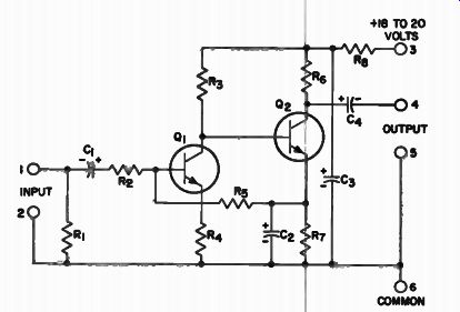
Fig. 72 - Schematic diagram and parts list for the microphone preamplifier.
--------------------
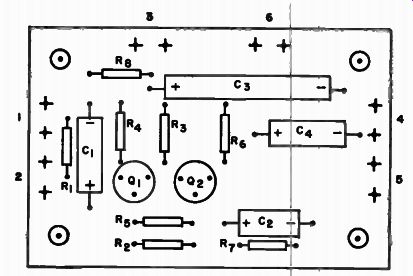
Fig. 73 - Component placement diagram for the microphone pre-amplifier.
-------------------
Special Considerations
When the preamplifier is used with a low-impedance dynamic microphone (such as the RCA-H K97 in the low impedance mode), R1 should be 220 ohms; when a microphone with an impedance of a pout 30,000 ohms is used (such as the RCA-HK97 in the high-impedance mode), R1 should be 270,000 ohms.
Construction
The drilling template for the micro phone preamplifier is shown at the back of this Manual; a component placement diagram and a photograph of the completed circuit board are shown in Figs. 73 and 74, respectively.
A single preamplifier circuit fits on a 3 by 2-inch circuit board; two can be built on a 3- by 4- inch board, and three on a 3- by 6- inch board. If the circuit is not constructed on a board, a ground bus should be used to ground the preamplifier to the circuits that follow it at one point only, preferably at the input to the circuits.
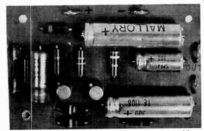
Fig. 74 Completed circuit board for the microphone preamplifier.
CIRCUIT NO. 8 - AUDIO MIXER, COMPRESSOR, AND LINE AMPLIFIER
Fig. 75 - A suggested enclosure for the audio mixer, compressor, and line-amplifier circuit.
The audio mixer, compressor, and line amplifier is an indispensable piece of equipment for the audio enthusiast who requires uniform audio levels such as are necessary in the production of very-high-quality tape recordings. Fig. 75 is a photograph of a suggested enclosure for this circuit.
Circuit Operation
The schematic diagram and parts list for the audio mixer, compressor, and line amplifier are shown in Fig. 76.
The circuit consists of a four-channel resistive mixer, an MOS transistor (Q1) that acts as a voltage-variable resistor, a high-impedance MOS transistor amplifier (Q 2 ), and a two-stage bipolar line driver. The characteristics of an MOS field-effect transistor that make it useable as a voltage-variable resistor are discussed in the section on Theory and Operation of Solid-State Devices; Q1 operates as described and, with R5, forms an incoming-signal voltage divider.
------------------
Parts List
C1 C2 C3 C7 = 0.1 microfarad, paper
C4 = 10 microfarads, 12 volts, electrolytic
C5 = 15 microfarads, 6 volts, electrolytic
C8 = 5 microfarads, 25 volts, electrolytic
C8 50 microfarads, 25 volts, electrolytic
CR 1 CR 2 = silicon rectifier, type 1N270 MOS field-effect transistor, type 3N128 transistor, RCA SK3020 Q1 Q2 = Q 3 Q 4 = R13 R10 = R11 = R12 = R14 = R15 = R16 = R17 = R1 R2 R3 R4 R7 = 100,000 ohms, 1/2 watt, 10% R5 = potentiometer, 10,000 ohms, audio taper R8 = 180,000 ohms, 1/2 watt, 10% R8 = potentiometer, 5000 ohms, straight taper R9 R13 = 1 megohm, 1/2 watt, 10% 15,000 ohms, 1/2 watt, 10% 10,000 ohms, 1/2 watt, 10% 1500 ohms, 1/2 watt, 10% 1200 ohms, 1/2 watt, 10% 100,000 ohms, 1/2 watt, 10% 470 ohms, 1/2 watt, 10% 2 megohms, 1/2 watt, 10%
-------------
Fig. 76 - Schematic diagram and parts list for the audio mixer, compressor,
and line amplifier.
--------
Circuit inputs are designed to be driven by the preamplifier circuit described in Circuit No. 7 or from any source capable of providing a 50- to 1000-millivolt signal. The gain of each input can be controlled by use of a 50,000-ohm potentiometer between the output of the preamplifier or other source and the input of the mixer stage.
Potentiometer R1, is the master gain control; it controls all channels simultaneously.
The initial bias voltage for Q1 is set by adjustment of potentiometer R8.
When Q1 is biased off, it has an effective drain-to-source resistance of several megohms. This high resistance allows nearly all of the signal voltage appearing at the potentiometer arm of R5 to appear at the gate of Q. The signal is amplified cy Q6 and passed to the output-amplifier and line-driver transistors Q3 and Q. The output signal of Q4 is rectified by CR2 and the resultant dc signal is fed back to the gate of Q. The rectified output signal is polarized in such a way that its application to Q1 reduces the drain-to source resistance of that transistor.
The result is a reduced input to Q2 and an over-all reduction in amplifier gain.
CR1 is inserted in the feedback line so that the rectified dc signal can be applied very rapidly to the gate of Q1 and to C3 . During this application, Cs is charged at a very fast rate. The discharge time of C3 is slow because CR1 forces the discharge current to flow through R18. The product of this arrangement of CR1, R18, and C3 is a circuit that has a fast attack time and a relatively slow release time. A fast attack time is a very desirable characteristic in a circuit of this type because it provides for immediate reduction in system gain and consequent prevention of the overload that could occur with a loud passage of speech or music. The delayed release time helps to maintain a constant level of output during small pauses in speech or music.
Q4 is connected as an emitter-follower to provide the amplifier with a low output impedance. The line driver is designed for operation at approximately 1 volt rms into a line of 250 ohms. The circuit can be adjusted so that any input signal level between 50 millivolts and 1 volt will result in an output of approximately 1 volt. Circuit current drain is about 23 milliamperes at 20 volts.
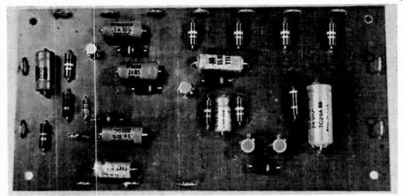
Fig. 77 - Completed circuit board for the audio mixer, compressor, and line
amplifier.
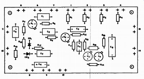
Fig. 78 - Component placement diagram for the audio mixer, compressor, and
line amplifier.
Construction
The drilling template for the audio mixer, compressor, and line amplifier is shown at the back of this Manual; a photograph of the completed circuit board and a component placement diagram are shown in Figs. 77 and 78, respectively.
CIRCUIT NO. 9 -- UNIVERSAL TIMER
The universal timer turns an electrical device off after a predetermined period of time. Because of the high impedance of the MOS field-effect transistor featured in the circuit, electrically and physically smaller, more stable timing capacitors can be used.
Circuit Operation
The schematic diagram and parts list for the universal timer are shown in Fig. 79. When switch S1 is activated (S u, open and S le, closed), capacitors C1 and C8 charge through diodes CR1 and CR2 , respectively; the voltage across C2 is applied to the gate of triac Q• through R6 and R13 and turns Q4 on.
The voltage across C2 is also applied to the timing-circuit elements R8 and C4; the voltage across Re and C4 (and consequently circuit timing) can be adjusted by R3 . C3 filters the voltage across R8 and C.. When the voltage across capacitor C4 is high enough, Q1 starts to conduct and the MOS transistor turns on and places a forward bias on the base-emitter junction of transistor Q2 . As a result, transistor Q2 turns on and triggers the regenerative switch composed of transistors Q2 and Q. When the regenerative switch conducts, it provides a means for the current to bypass the gate of the triac, Q., and the triac turns off, thus depriving the load of power. The timer circuit remains in this state until switch S1 is opened at least momentarily.
S1, a double-pole double-throw switch, is wired so that the C. discharge circuit is completed when the line-power circuit is opened. This arrangement allows C4 to discharge rapidly through R9 and permits the timer to be recycled almost immediately.
----------
Parts List
C1 = 10 microfarads, 200 volts, electrolytic
C2 10 microfarads, 200 volts, electrolytic
C3 = 50 microfarads, 15 volts, electrolytic 4 microfarads, see text
= 0.01 microfarad, 25 volts or greater, 10%
CR1 CR2 = silicon rectifier, RCA SK3031
F1 = fuse, size depends on expected load
Q1 = MOS field-effect transistor, type 3N128 transistor, RCA SK3005 transistor, RCA SK3020 triac, RCA 40503 or RCA 40429 (the RCA 40429 may be C4 = C6 C6 Q2 =Q3 = Q 4 = used with Wakefield No. NC401K or equivalent heat sink.)
R1 R8 = 100 ohms, 1/2 watt, 10% R2 = 15,000 ohms, 1/2 watt, 10% R.3 = potentiometer, 10,000 ohms, linear taper 1000 ohms, 1/2 watt, 10% 3000 ohms, 5 watts, 10% 390 ohms, 1/2 watt, 10% 4.7 megohms, 1/2 watt, 10%, see text R8 = 5.6 ohms, 1/2 watt, 10% = 3900 ohms, 1/2 watt, 10% = 150 ohms, 1/2 watt, 10% It 12 R13 = 470 ohms, 1/2 watt, 10% S1 = switch, 125 volts, double-pole, double-throw, capable of handling the expected load.
R4 = R6 - R7 - R8 = R10 R11
-----
Fig. 79 - Schematic diagram and parts list for the universal timer.
----
Special Considerations
If a wider range of time periods is desired than can be obtained with potentiometer R 3 alone, a selector switch may be used to permit various values of R8 or C4 to be switched in.
Electrolytic capacitors should not be used for C4, and R8 should not exceed 100 megohms; otherwise, an unstable circuit will result. The maximum time period attainable (in seconds) is equal to the product of the values of R8 (in ohms) and C4 (in microfarads) divided by 1.59.
The amount of power that the timer circuit can handle depends on the ratings of the triac and the type of heat sink used. The RCA-40429 triac can handle a load current of 2.7 amperes without a heat sink; when mounted on a suitable heat sink (Wakefield No. NC 401K or equivalent), it can handle 6 amperes. The RCA-40503 is supplied with a factory-attached heat radiator that allows it to conduct a maximum of 3.3 amperes. The section on Mechanical Considerations contains a further discussion of heat sinks.
The MOS transistor leads should be shorted until the timing components, R8 and C4, are connected. This precaution prevents damage to the MOS transistor. (See the section on Mechanical Considerations for MOS transistor handling techniques).
Construction
Fig. 80 - Completed circuit board for the universal timer.
Fig. 81 - Component placement diagram for the universal timer.
One critical feature in the layout of this circuit is the placement of R6. This resistor generates heat and should not be located close to other components.
The suggested layout shown in Fig. 81 should be used if possible.
A second critical feature involves the placement of the time-determining components R8 and C4. These components and the associated wiring should be shielded as much as possible from dust and dirt that could provide leak age paths and affect circuit timing.
The drilling template for the universal timer is shown at the back of this Manual; a photograph of the completed circuit board and a component placement diagram are shown in Figs. 80 and 81, respectively.
CIRCUIT NO. 10- ENLARGER EXPOSURE METER
The exposure meter, a light intensity meter, provides an excellent means for accurately setting exposure when using an enlarger.
In operation, the required exposure time must first be determined experimentally with a test negative. When this time is established, the photocell of the exposure meter is placed on the easel over the center of interest and the meter is adjusted for zero deflection.
The negative to be printed is then inserted into the enlarger carrier and the iris of the enlarger is adjusted so that zero meter deflection is again attained. The photocell of the exposure meter is then removed and the printing paper is inserted and exposed for the predetermined period of time.
-------------
Parts List
CR1 CR2 CR8 CR 4 =silicon rectifier, type 1N270 M = meter, 0 to I milliampere, 12 volt, or 0 to 500 microamperes, 9 volt Photocell = RCA KD2106 Q IQ 2 = transistor, RCA SK3020 RiR2R7 = 4700 ohms, 1/2 watt, 10% R8 = R4 = Re. = RO = R8 = Si = 2200 ohms (12 volts), 3300 ohms (9 volts), 1/2 watt, 10% 47,000 ohms, 1/2 watt, 10% 100,000 ohms, 1/2 watt, 10% 10,000 ohms, 1/2 watt, 10% potentiometer, 50,000 ohms, linear taper range switch, single-pole, double-throw
--------
Fig. 82 - Schematic diagram and parts list for the enlarger exposure meter.
--------
The enlarger exposure meter is equipped with a range switch so that it can accommodate either high- or low-intensity light. On the low scale the meter can be adjusted for zero at light intensities of 0.2 to 6 footcandles; on the high scale, zero deflection is attainable between 6 and 400 foot-candles.
Circuit Operation
The schematic diagram and parts list for the enlarger exposure meter are shown in Fig. 82 Transistors Q1 and Q2 and resistors R1 and R2 form a bridge circuit. The meter connected between the collectors of Q1 and Q2 registers zero deflection when a balanced bridge condition is met. The bridge rectifier assembly composed of rectifiers CR1 through CR, permits the meter to record both positive and negative unbalance currents. Resistors R R2, and R3 are designed for full-scale meter deflection with maximum unbalance current.
Special Considerations
The 9 or 12 volts needed to operate the exposure meter may be obtained from batteries or a power supply. The maximum current drain of the circuit at 12 volts is 3 milliamperes. The maximum current drain at 9 volts is 1.5 milliamperes.
With a 12-volt supply a 1-milliampere meter movement should be used; for a 9-volt supply a 500-microampere meter movement should be used.
Construction
The drilling template for the enlarger exposure meter is shown at the back of this Manual; a photograph of a completed circuit board and a component placement diagram are shown in Figs. 83 and 84, respectively. Fig. 85 shows a method of mounting the photocell in a block of plastic; the alligator clips are clipped to the appropriate circuit-board terminals.
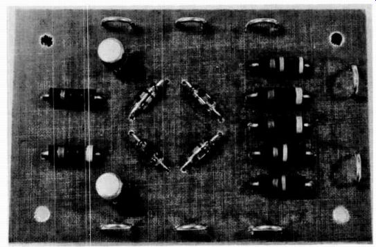
Fig. 83 - Completed circuit board for the enlarger exposure meter.
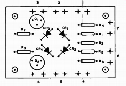
Fig. 84 - Component placement diagram for the enlarger exposure meter.
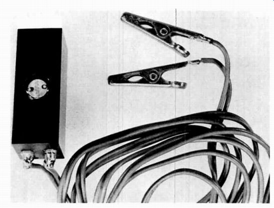
Fig. 85 - A suggested method of mounting the photocell in a block of plastic.
CIRCUIT NO. 11 - LAMP DIMMER
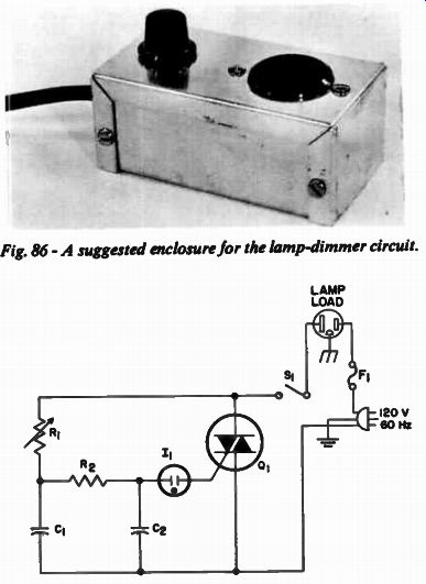
Fig. 86 - A suggested enclosure for the lamp-dimmer circuit.
------------ Parts List
C1 C2 = 0.068 microfarad, 200 volts, 10% F1 = fuse, size suitable to load Ii = lamp, neon type NE-83 Q1 - triac, RCA 40502 or RCA 40429 (the RCA 40429 may be used with the Wakefield No. NC401K or equivalent heat sink.) R1 = potentiometer, 50,000 ohms, 2 watts, linear taper R2 = 15,000 ohms, 1/2 watt, 10%, carbon S1 = switch, 120 volt, single-pole, single-throw, capable of handling expected load current
-------
Fig. 87- Schematic diagram and parts list for the lamp dimmer.
---------
The lamp-dimmer circuit provides continuous control of loads up to 700 watts. With it, incandescent lamps can be set at any level up to their maximum brightness. Fig. 86 shows a suggested enclosure for the lamp-dimmer circuit.
Circuit Operation
The schematic diagram and parts list for the lamp dimmer are shown in Fig. 87. The solid-state device used in the lamp-dimmer circuit is a triac, a type of thyristor that can conduct in either direction and thus permits full wave control of the load. The triac is triggered into conduction on each half cycle by a pulse applied to its control lead, the gate. The power delivered to the load is a function of the time in each half-cycle at which the triac is triggered into conduction. The point at which the triac is triggered on each half-cycle is determined by C1 , C2 , R2 , and the potentiometer R1 . When the capacitors charge to the triggering level of the neon lamp I I , conduction into the gate of the triac occurs. The triac then conducts for the remainder of that half cycle.
The RCA-40429 triac can handle 2.7 amperes without a heat sink; the RCA-40502 triac can handle 3.3 amperes with its factory-attached radiator. At current levels above these values, the triac must be fitted with a heat sink, such as Wakefield No. NC401K or equivalent. Under no circumstances should load current exceed 6 amperes in this circuit. The section on Mechanical Considerations contains a discussion of heat sinks. Any radio interference produced by the lamp dimmer can be reduced by use of the L filter described in Circuit No. 29.
Construction
Because of the small number of components used in this circuit, the layout is left to the circuit builder.
CIRCUIT NO. 12 - TEMPERATURE ALARM
The temperature indicator is an extremely sensitive device that can differentiate fractions of a degree of temperature. A flashing lamp indicates when a predetermined temperature has been reached. Because the circuit can be wired to warn of temperature increases or decreases, it is of practical use as a road-icing indicator for motorists, a frost-warning indicator for farmers, or an indicator to warn of rising temperatures in freezers.
Circuit Operation
The schematic diagram and parts list for the temperature alarm is shown in Fig. 88. The circuit is wired to signal a decrease in temperature below a predetermined level. Transistor pairs Q4-Q5 and Q6-Q7 each form a voltage-dependent regenerative switch.
With the circuit wired as shown in the schematic, the triggering level of the Q4-Q3combination is determined by the thermistor; the triggering voltage of the Q6-Q7 combination is con trolled by the sensitivity potentiometer R15 and the resistor in series with it, R13. The two regenerative switches are in parallel; both are driven by Q3 from the same intermittent voltage. Q3 is switched on and off by the multivibrator composed of transistors Q1 and Q2 ; a basic multivibrator is discussed in the section on General Circuit Considerations. The intermittent voltage assures that the triggering voltages of the regenerative switches will be sampled once per second so that the switch with the lowest triggering voltage will conduct during the next second. If this sampling were not performed, the first regenerative switch to conduct would continue to do so regardless of the characteristics of the second switch.
As long as the thermistor resistance is lower than that of the R13 -- R,6 combination, the triggering voltage of the regenerative switch composed of Q4 and Q 5 is lower than that of the Q6- Q 2 combination and the thermistor controlled switch conducts, effectively shorting out the regenerative switch composed of transistors Q6 and Q2. As thermistor resistance increases (through cooling), the triggering voltage of Qe and Q2 approaches and finally becomes less than that of the Q4- Q5 combination. When Q6 and Q7 are triggered, they short out the Q4 - Q8 switch and permit current to flow to the base of Q8. Q8 then turns on and conducts current to the lamp. The fact that regenerative-switch triggering voltages depend on the resistance of the thermistor or sensitivity potentiometer means that circuit operation is independent of fluctuations of voltage in the power supply.
------------------
Parts List
C1 C2 = 15 microfarads, 15 volts, electrolytic
Cs = 50 microfarads, 15 volts, electrolytic
C4 C8 = 0.01 microfarad Q5 Q 7 Q8 = transistors, RCA SK3020
Q1 Q2 Q3 Q4 Q6 = transistors, RCA SK3005
Lamp = No.47 Ri R5 R13 = 1000 ohms, 1/2 watt, 10% R2 R3 = 39,000 ohms, 1/2 watt, 10% R4 = 82 ohms, 1/2 watt, 10% R3 = 330 ohms, 1/2 watt, 10% R7 R14 = 18 ohms, 1/2 watt, 10% R8 Rio = 470 ohms, 1/2 watt, 10% R81211 = 150 ohms, 1/2 watt, 10% R12 = 68 ohms, 1/2 watt, 10% R18 = potentiometer, 10,000 ohms, linear taper
Thermistor = RCA KD2 108 (supplied in RCA Kit KD2 1 10)
-----------
Fig. 88 - Schematic diagram and parts list for the temperature alarm.
---------
To modify the circuit so that the lamp will light with an increase in temperature, it is necessary to inter change the thermistor and the sensitivity potentiometer R18 and to connect R13 between C4and terminal No. 5. The connection between C5 and terminal No. 4 will be straight wire. The current drain for this circuit averages about 20 milliamperes.
Adjustment and Operation
For adjustment of the circuit so that the indicator lamp will flash when the temperature of interest has been reached, the thermistor is placed in a temperature environment similar to that at which the circuit will be expected to give warning. The potentiometer shaft is then rotated until the lamp just stops flashing. At this point the circuit is set to warn of the temperature of interest.
The schematic diagram and parts list for the temperature-alarm power supply are shown in Fig. 89. The power supply features a floating battery that insures circuit operation in spite of utility-company power failures. Diode CR, isolates the battery from the secondary voltage of T1. Q1 does not require a heat sink in this application.
The power supply transformer should have a dc resistance in the secondary of at least 1 ohm. If it does not, a 1-ohm 2-watt resistor should be inserted in series with the secondary. If a center-tapped supply is used, the resistance should be placed in series with the center tap. No special precautions are required if the transformer specified in the parts list is used.
---------------
Parts List
C1 = 4000 microfarads, 25 volts, electrolytic C2. 100 microfarads, 15 volts, electrolytic C5 = 0.1 microfarad, 25 volts or greater
CR1 CR 2 CR 3 = silicon rectifier, RCA SK3030
CR4 - zener diode, 10 volts, 1 watt F1 = Q1 = Q2 = S1 = T1 fuse, 1 ampere, 125 volts transistor, RCA SK3027 transistor, RCA SK3020 switch, 125 volts, 1 ampere, single-pole, single-throw = transformer, 115 volts primary, 30 volts secondary with center tap, Stancor No. TP-4 or equivalent
-------
Fig. 89 - Schematic diagram and parts list for the temperature-alarm power
supply.
--------
Fig. 90 - Component placement diagram for the temperature alarm.
--------------
Construction
No special precautions need be observed in the construction of this circuit except that the physical and electrical size of the sensitivity potentiometer should be determined by the application in which the circuit is to be used. In most applications the thermistor, the sensitivity potentiometer R15, and the lamp will not be mounted on the circuit board. Thermistor mounting is discussed in the section on Mechanical Considerations.
The drilling template for the temperature alarm is shown at the back of this Manual; a component placement diagram and a photograph of the completed circuit board are shown in Figs. 90 and 91, respectively.
Fig. 91 - Completed circuit board for the temperature alarm.
CIRCUIT NO.13-POSITIVE-ACTION LIGHT-OPERATED SWITCH
------------
Parts List
6 C1 = 5 microfarads, 15 volts, electrolytic
CR1 = silicon rectifier, RCA SK3031
CR2 = silicon rectifier, RCA SK3030
F1 = fuse, 3 amperes
Photocell = RCA KD2016
Q2 = transistor, RCA SK3005
Q2 ... transistor, RCA SK3020 2
R1 = 150 ohms, 1/2 watt, 10%
R2 = 5600 ohms, 2 watts, 10%
R3 = 470 ohms, 1/2 watt, 10%
R4 = potentiometer, 250 ohms, linear taper
Relay = 12 volts, 1350 ohms, Potter and Brumfield No. RS5D or equivalent
S1 = switch, 125 volts, 3 amperes, single-pole, single-throw
--------------
The positive-action photo or light operated switch can control loads rated at up to 2 amperes. Positive action means that the load is receiving either no power or full power; current to the load does not fluctuate with the amount of light impinging on the photocell. The switch works directly from 120-volt household power, eliminating the needs for batteries. The light level needed to energize the switch can be set by the circuit builder to the value best suited to his application. This switch turns off with an increase in light.
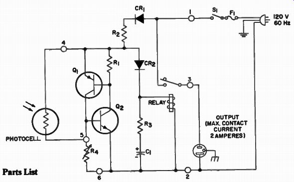
Fig. 92 - Schematic diagram and parts list for the positive-action light-operated
switch.
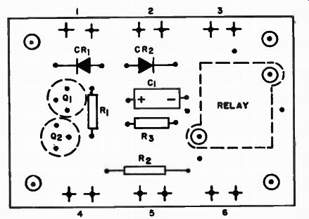
Fig. 93 - Component placement diagram for the positive-action light-operated
switch.
Circuit Operation
The schematic diagram and parts list for the photo-switch are shown in Fig. 92. Transistors Q1 and Q2 form a regenerative switch that exhibits high impedance until the voltage across it reaches a predetermined level. When this level is reached, the switch triggers and its impedance becomes very low.
The triggering voltage required is determined by the resistance of the photocell and the setting of the potentiometer R4. When the photocell is exposed to light, its resistance decreases and causes an increase in current to the base of Q2. When the base current is sufficient, Q2 conducts and triggers the regenerative switch into conduction. Because voltage across the regenerative switch is half wave rectified ac (CR1 is the rectifying diode), the regenerative switch can be triggered on each positive half-cycle. If the photocell is not exposed to light, the regenerative switch will not trigger.
The relay which is connected across the regenerative switch operates as long as the regenerative switch is not conducting. As soon as the regenerative switch conducts, the relay releases. The relay contact rating is 2 amperes.
Construction
The drilling template for the positive-action light-operated switch is shown at the back of this Manual; a component placement diagram and a photograph of a completed circuit board are shown in Figs. 93 and 94, respectively.
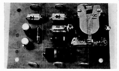
Fig. 94 - Completed circuit board for the positive-action light-operated switch.
CIRCUIT NO. 14 - MOISTURE-CONTROLLED SWITCH
The moisture-controlled switch energizes loads up to 1000 watts when a moisture level predetermined by the user is detected. This circuit cannot be used when the moisture being detected is grounded.
Circuit Operation
The schematic diagram and parts list for the moisture-controlled switch are shown in Fig. 95. The circuit turns on power to a load with an increase in moisture level. Transistor pairs Q1 - Q2 and Q3 -Q4 each form a voltage - dependent regenerative switch; the function of the switches is to control the signal voltage to the gate of SCR2.
With the circuit wired as shown in the schematic, the triggering level of the Q1-Q2 combination is determined by the resistance between the probes and R13 ; the triggering voltage of the Qs - Q4 combination is controlled by the combination of Ra and R2.An intermittent 60-Hz voltage, half-wave rectified by CR 2 is placed across the paralleled regenerative switches. The intermittent voltage assures that the triggering voltages of the regenerative switches are tested 60 times per second so that the switch with the lowest triggering voltage will conduct during the next cycle. If this testing were not performed, the first regenerative switch to conduct would continue to do so regardless of the characteristics of the second switch.
--------------
Parts List:
C1 = 10 microfarads, 15 volts, electrolytic
C2 = 200 microfarads, 6 volts, electrolytic , see text
CR1 CR2* = silicon rectifier, RCA SK3031
CR3 CR4* = silicon rectifier, RCA SK3030
F1 = fuse, 120 volts, rating determined by the load, maximum 10 amperes
Q1 Q4 = transistor, RCA SK3020
Q2 Q3 = transistor, RCA SK3005
R1 R3 = 4700 ohms, 2 watts, 10%
R2 = 270 ohms, 1/2 watt, 10%
R4 = 180 ohms, 1/2 watt, 10%
R5 R12 = 470 ohms, 1/2 watt, 10%
R6 R11 = 1500 ohms, 1/2 watt, 10%
R7 12, 5 = 22,000 ohms, 1/2 watt, 10%
R.5 = 10,000 ohms, 1/2 watt, 10%
R3 = potentiometer, 50,000 ohms, linear taper
R13 = 1000 ohms, 1/2 watt, 10%
0 to 250 ohms, 1/2 watt, 10%, see text
S1 - switch, 125 volts, single-pole, single-throw
SCR1
SCR2* = silicon controlled rectifier, RCA KD2100
R 14 =
*All SCR's and rectifiers are available in the RCA KD2105
Experimenter's Kit. Two Kits are needed.
------------------
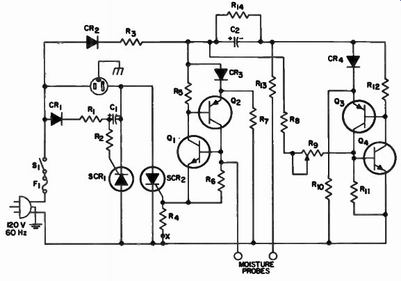
Fig. 95 -- Schematic diagram and parts list for the moisture-controlled switch.
---------------
As long as the total resistance of R13 and the resistance between the probes is lower than that of the R8 - R9 combination, te triggering voltage of the regenerative switch composed of Q1 and Q2 is lower than that of the Q3 - Q4 combination and the switch con trolled by probe resistance conducts, effectively shorting out the regenerative switch composed of transistors Q3 and Q. As the total resistance of R13 and the resistance between the probes increases, the triggering voltage of Q1 and Q2 approaches and finally becomes more than that of the Q3 Q4 combi nation. When Q3 and Q4 are triggered, they short out the Q1- Q2 switch and permit current to flow to the gate of SCR,. When a sufficient signal is applied to the gate of SCR2 , it turns on and applies a voltage to the load and the network composed of diode CR,, resistor R1 , and capacitor C1, and causes C1 to charge. During the next half-cycle of voltage, the charge on C1 is applied to the gate of SCR, and turns it on. This process repeats as long as a sufficient signal is applied to the gate of SCR2 . When there is no moisture at the probes, the triggering level of the re generative switch composed of Q1 and Q2 becomes high, and the Q3-Q4 switch turns on and places a voltage across R1. This voltage drop causes a slight decrease in the firing potential of the Q1-Q2 switch and changes the difference between the "turn-on" and "turn-off" moisture levels. Therefore, the sensitivity of the circuit may be varied by changing the value of R14 ; for maximum sensitivity R14 and C2 may be omitted and replaced by a jumper.
Connected as described above, the moisture-controlled switch supplies power to a load with an increase in moisture level. To have the circuit turn off power to the load with an increase in moisture level requires that the junction of R3 and the emitter connection of Q1 be moved from the gate of SCR2 to the lower end of R4 (point X); the junction of R1, and the emitter connection should then be connected to the gate of SCR2 . Construction The full power-handling capabilities of this circuit can be realized only when the SCR's are provided with heat sinks. The RCA KD2100 SCR comes mounted on a heat-sink bracket and is electrically insulated from the bracket.
The type of probe used is a function of the amount of moisture to be detected; liquid moisture can be detected with probes consisting of bare wires. For proper circuit operation the probes should not be grounded through the moisture being detected.
A suggested method of building this circuit in a 3- by 4- by 5-inch aluminum box is shown in Fig. 96.
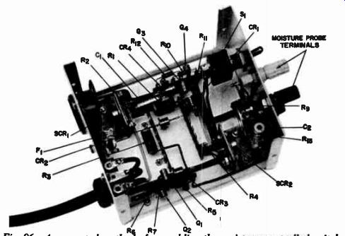
Fig. 96 - A suggested method of assembling the moisture-controlled switch.
Components not shown are hidden.
CIRCUIT NO. 15--ELECTRONIC FUZZ BOX
The fuzz box is intended to be used with a guitar; however, it may be used with any instrument whose musical output is electrically amplified. It can be used with the audio power amplifier circuit described in this Manual. The fuzz box changes the character of the sound produced by an instrument and makes possible the generation of a variety of sounds of which the instrument alone is not capable.
Circuit Operation
The schematic diagram and parts list for the electronic fuzz box are shown in Fig. 97. The output of transistor Q1, a basic emitter-follower that gives the fuzz box a high-impedance input, is applied to the base of Q2 . Q2is biased at almost cutoff and, therefore, amplifies only half the input signal.
Potentiometer R6 is used to adjust the ...
--------------
Parts List
C1 = 0.01 microfarad, 25 volts or greater
C2 C2 C4 = 5 microfarads, 15 volts, electrolytic
Q1 Q3 = transistor, RCA SK3020
Q2 = transistor, RCA SK3005
R1 R2 R3 R7 = 100,000 ohms, 1/2 watt, 10%
R4 = 3300 ohms, 1/2 watt, 10%
R5 = potentiometer, 5000 ohms, linear taper
R6 = 15,000 ohms, 1/2 watt, 10%
R8
R10 = 2700 ohms, 1/2 watt, 10%
Rs = 47,000 ohms, 1/2 watt, 10%
R11 = potentiometer, 10,000 ohms, linear taper
S1 = switch, double-pole, double throw
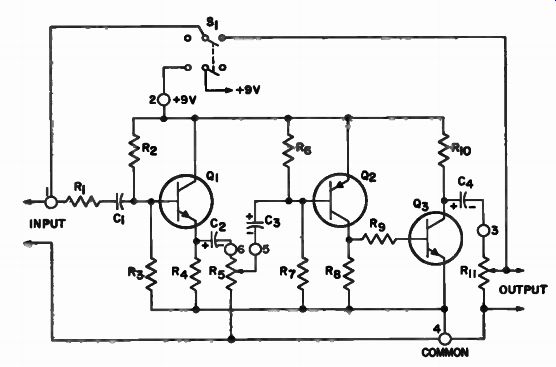
----- Fig. 97 - Schematic diagram and parts list for the electronic fuzz
box.
------
... input signal level to Q2 (to approximately 1 volt) and the amount of "fuzz." Transistor Q3 receives the output from Q2 through R3; Q3 is biased in such a way that the top half of the signal input to it is clipped; this clipping action tends to create a square wave. Potentiometer R11 is used to vary the output level of the circuit.
The input voltage of this circuit should be approximately 1 volt. The current drain for this circuit is approximately 5 milliamperes.
Construction
In operation, the fuzz box is normally cut in and out as music is being played. When the fuzz box is cut out the musical instrument is connected directly to the amplifier.
The drilling template for the electronic fuzz box is shown at the back of this Manual; a component placement diagram and a photograph of a completed circuit board are shown in Figs. 98 and 99 respectively.
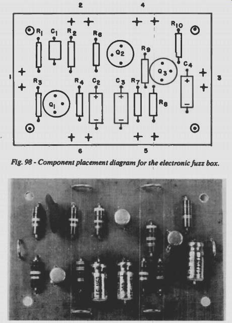
Fig. 98 - Component placement diagram for the electronic fuzz box. Fig. 99 - Completed circuit board for the electronic fuzz box.
CIRCUIT No. 16 - PHONOGRAPH PREAMPLIFIER
The phonograph preamplifier can be used with the audio power amplifier of Circuit No. 17 to provide an excel lent high-fidelity system. The preamplifier is designed for use with a magnetic pickup capable of supplying an input signal of at least 5 millivolts and has provisions for tape and tuner input.
At the 5-millivolt signal level, the preamplifier delivers an output of at least 1 volt.
Circuit Operation
The schematic diagram and parts list for the phonograph preamplifier are shown in Fig. 100. Transistor Q1 is a low-noise transistor and is directly coupled to Q2. A frequency-shaping network in the feedback circuit of Q2 provides frequency compensation when the preamplifier is used with a magnetic phonograph pickup. The output circuit of Q2 contains a level control R10 that feeds the loudness control S2 through the selector switch S1. The loudness control, in turn, drives the tone-control circuits of the preamplifier. Tape, tuner, or phono inputs can be selected by means of the selector switch; a connector in the arm of the selector switch permits tape recordings to be made without affecting volume or loudness and vice versa.
------------
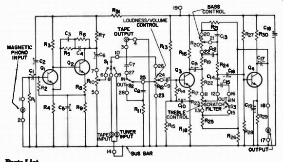
Fig. 100 - Schematic diagram and parts list for the phonograph preamplifier.
------
Parts List
C1 = 2 microfarads, 6 volts, electrolytic
Cs C17 C18 = 25 microfarads, 25 volts, electrolytic
C3 = 0.0027 microfarads, 200 volts, paper
0.01 microfarads, 200 volts, paper
C5 = 100 microfarads, 3 volts, electrolytic
C5 1 microfarad, 25 volts, electrolytic 180 picofarads, 500 volts, mica
0.033 microfarad, 200 volts, paper C
C7 = C8 = C9 = 1 microfarad, 12 volts, electrolytic C io C 16 = 10 microfarads, 10 volts, electrolytic C11 = 10 microfarads, 25 volts, electrolytic C12 C13 = 0.022 microfarad, 200 volts, paper
0.0039 microfarad, 200 volts, paper
0.0047 microfarad, 200 volts, paper 100 microfarads, 6 volts, electrolytic C14 = C15 = C19 =
Q1 Q2 Q3 Q4 = transistor, RCA SK3020
R1 R3 = 68,000 ohms, 1/2 watt, 10%
R2 = 180,000 ohms, 1/2 watt, 10%
R4 = 470 ohms, 1/2 watt, 10%
R5 = 27,000 ohms, 1/2 watt, 10%
R6 = 470,000 ohms, 1/2 watt, 10%
R7 R19 R 2 1
R24 = 10,000 ohms, 1/2 watt, 10%
R8 = 82 ohms, 1/2 watt, 10%
R9 = 1,800 ohms, 1/2 watt, 10%
R10 = potentiometer, 100,000 ohms audio taper, Centralab
Fi -
100K or equivalent
R11 = 8,200 ohms, 1/2 watt, 10%
R12 = potentiometer, 250,000 ohms, audio taper with tap, Centralab F11-250K or equivalent R13 33,000 ohms, 1/2 watt, 10% R 14 R28 = 18,000 ohms, 1/2 watt, 10% R1 3 R31 = 4,700 ohms, 1/2 watt, 10% R16 = 6,800 ohms, 1/2 watt, 10% R17 = 68 ohms, 1/2 watt, 10%
R18 R22 R25 R29 = 1,000 ohms, 1/2 watt, 10% R20 R23 = potentiometer, 100,000 ohms, straight taper, Centralab F1-100K or equivalent, 1/2 watt, 10% R23 = 47,000 ohms, 1/2 watt, 10% R2 7 = 56,000 ohms, 1/2 watt, 10% R30 = 2,700 ohms, 1/2 watt, 10% S1 = switch, single pole, 3-position, wafer S2 = switch, single-pole, double throw, toggle S3 = switch, single-pole, single-throw, toggle
--------------------------
Fig. 101 shows the response of the treble and bass tone controls as a function of frequency. Boost of 10 dB and cut of 15 dB are available for deep bass and high treble frequencies. Each control operates independently so that precise tone shaping is possible. When both controls are in the center position, the response is flat; the bass and treble frequencies are equally mixed.
Output distortion is low at all frequencies for any setting of either the bass or the treble tone control. The collector-to-base feedback in Q3 and Q4 works with the tone controls to provide the overall tonal response of the pre-amplifier.
Included in the preamplifier is a loudness/volume control switch S2.
With the loudness control in, lower tones are enhanced at low output levels and a more pleasing sound is produced; when the loudness control is switched out, the volume control attenuates all tones equally, as shown in Fig. 102 (a). The scratch filter attenuates some what the frequencies at which scratch noise from scratched records is most ...
Fig. 101 - Response of treble and bass tone controls as a function of frequency.
... prevalent. Fig. 1C2 (a)shows frequencies attenuated by the scratch filter; Sa controls the filter. Fig. 102 (b) compares the measured response of the preamplifier with an ideal response.
A magnetic-pickup level control is provided so that the preamplifier does not have to be readjusted when the input is changed from magnetic phono graph to tape, for example.
DC power for the preamplifier can be obtained from a 20-volt power supply or from the audio power amplifier supply (Circuit No. 17) through the RC circuit shown in Fig. 103. A 300 millivolt input level from a tuner or tape recorder is required to produce a 1-volt output; a 5-millivolt input level is required from a magnetic phono graph pickup to produce the same output. The current drain for the phonograph preamplifier is 7.5 milliamperes at 20 volts.
Construction
To keep the hum level at a minimum, a requirement in any high-gain audio system, a progressive grounding method or common bus has been used.
In this system, shown in Fig. 104, a bus wire made from a length of No. 18 wire is connected between the common input and the common output terminals. All grounds of the preamplifier circuit are then connected to this common bus.
Fig. 102 - (a) Effect of loudness control and scratch filter, and ( b) comparison
of measured response with ideal response.
If the preamplifier is used by itself, the external ground connection can be made at either end of the bus bar, whichever produces the lowest hum level. If the preamplifier is used with the audio power amplifier, the preamplifier is grounded through the power amplifier and no physical ground is made to the preamplifier itself.
The drilling template for the phonograph preamplifier is shown at the back of the Manual; a photograph of a completed circuit board and a component layout diagram are shown in Figs. 105 and 106, respectively.
Fig. 103 - RC circuit required to adapt the power supply of the audio power
amplifier (Circuit No. 17) to the phonograph preamplifier.
Fig. 104 - Back of phonograph preamplifier circuit board showing bus bar.
Fig. 105 - Completed circuit board for the phonograph preamplifier.
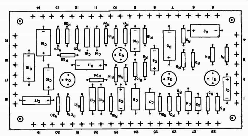
Fig. 106 - Component placement diagram for the phonograph preamplifier.
CIRCUIT NO. 17- AUDIO POWER AMPLIFIER
The general-purpose audio amplifier is capable of a power output of 7.5 watts and is compatible with all of the circuits in this manual. A suggested enclosure for the amplifier is shown in Fig. 107.
Circuit Operation
The schematic diagram and parts list for the audio power amplifier are shown in Fig. 108. This circuit is designed for use with the universal series supply (Circuit No. 1(a)); however, the simpler unregulated supply shown in Fig. 109 may also be used.
The output stage of the amplifier is a class B complementary-symmetry circuit that allows the speaker to be driven directly without the need of a transformer. The fundamental operation of a complementary-symmetry circuit can best be understood by examining the circuit conditions at three points in the output-voltage cycle; the point at which the instantaneous output voltage is zero (the dc condition), the point at which the voltage is peak positive, and the point at which the output voltage is peak negative. It is assumed that the frequency of operation is high enough to prevent a change in voltage across the capacitors during the output cycle.
When no signal voltage is applied to the circuit, the center-point voltage is 12 volts (the center point is indicated on the circuit schematic). The operating-point voltage of the driving transistor Q2, and consequently the dc voltage at the center point, is established by the beta and base-to-emitter voltage of Q2 and the values of resistors R2 , R5, R6, and R7. The bias voltage that establishes the idling or no-signal current in the output stage is developed across CR,. At idle, the diode voltage equals the base-to-emitter voltages of the two output transistors, Q3 and Q4 .
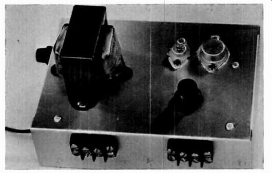
Fig. 107 - A suggested enclosure for the audio power amplifier.
When a negative signal is applied to Q1, the base current of Q2 is reduced.
The reduction in base current reduces the collector current of Q2 . Capacitor C4 maintains a constant voltage and, therefore, a constant current through R7. Because of this constant current in R7, the base current in Q3 increases by the same amount that the collector current in Q2 decreases. Q3 turns on and applies a positive voltage to C5 and the speaker load.
When a positive signal is applied to Q7, the base current of Q2 increases.
The higher base current, in turn, increases the collector current of Q2 . Then, because the current through R7 is constant, the additional current required in the collector of Q2 flows out of the base of Q4 and Q4 turns on.
----------
Parts List
C1 = 50 microfarads, 10 volts, electrolytic 250 microfarads, 25 volts, electrolytic Cs - 150 picofarads, 50 volts or greater 500 microfarads, 12 volts, electrolytic
C6 = 500 microfarads, 25 volts, electrolytic CR 1 germanium rectifier, type 1N3226 Q7 = transistor, RCA SK3020 Cg = Q2 = transistor, RCA SK3024 with heat sink, Wakefield NF209 or equivalent.
Q3 = transistor, RCA SK3026
Q4 = transistor, RCA SK3009 11 7
Re = 1000 ohms, 1/2 watt, 10%
R2 = 3300 ohms, 1/2 watt, 10%
R3 = 510 ohms, 1/2 watt, 10%
R4 = 10,000 ohms, 1/2 watt, 10%
R5 = 27,000 ohms, 1/2 watt, 10%
R6 R7 = 100 ohms, 2 watts, 10%
R9 = potentiometer, 5000 ohms, linear taper
Speaker = 8 ohms
---------
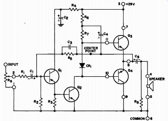
Fig. 108 - Schematic diagram and parts list for the audio power amplifier.
------
Parts List
C1 = 1000 microfarads, 50 volts, electrolytic
CR1 CR2 CR3 CR4 = silicon rectifier, RCA SK3030
F1 - fuse, 1 ampere, 125 volts
S1 - T1 = switch, 125 volts, 1 ampere, single-pole, single-throw filament transformer, 115 volts primary, 24 volts secondary, Triad No. F-45X or equivalent
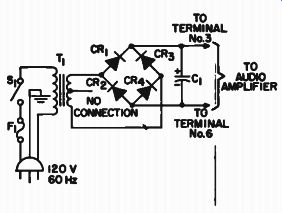
Fig. 109 - Simple unregulated supply for use with the audio power amplifier.
---------------
Capacitor C5 applies a negative voltage across the load through Q5. The frequency of the signal and the value of C5 and high enough so that the voltage of C5 goes through negligible change during the half-cycle.
Capacitor C3 reduces the crossover distortion through feedback. An input of approximately 0.5 volt is required for full power output. The current drain for this circuit is about 95 milliamperes with no signal.
Construction
The drilling template for the audio power amplifier is shown at the back of the Manual; a component placement diagram and a photograph of the interior of the suggested enclosure are shown in Figs. 110 and 111, respectively. The layout given is the best for this circuit.
Transistors Qa and Q4 are mounted external to the circuit board on a heat sink (Wakefield No. NC401K or equivalent) or on a metal chassis. The wires connecting Q3 and Q4 to the circuit board should be as short as possible so that there is no lead resistance and no possibility of capacitive coupling to other circuits. Transistor Q2 must be fitted with a heat radiator such as a Wakefield NF209 or equivalent.
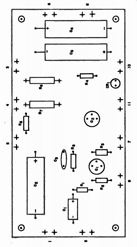
Fig. 110 - Component placement diagram for the audio power amplifier.
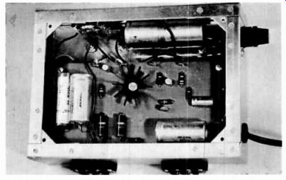
Fig. 111 - The interior of the enclosure suggested for the audio power amplifier.
The power-supply transformer should have a dc resistance in the secondary of at least 1 ohm. If it does not, a 1-ohm 2-watt resistor should be inserted in series with the secondary. If a center-tapped supply is used, the resistance should be placed in series with the center tap. No special precautions are required if the transformer specified in the parts list is used.
Under no circumstances should the output terminals be shorted when there is a signal applied to the input; a burned-out output transistor can result. To help protect the output transistor a 3/4-ampere slo-blo fuse may be inserted in the output circuit.
------
++++++++++++