(cont from part 1)
CIRCUIT NO. 18-ELECTRONIC METRONOME
The electronic metronome produces a series of audible "beeps" at a rate determined by the user. Its most common use is in metering musical cadence, but it may be used in the darkroom to measure time audibly. If the "beep" rate of the timer is set at 1 second, the passage of an amount of time can be noted by counting the "beeps." The electronic metronome has an advantage over the mechanical type in that it does not have to be rewound.
Circuit Operation
The schematic diagram and parts list for the electronic metronome are shown in Fig. 112. Transistors Q1 and Q2 form a regenerative switch that has a high impedance until it is triggered, when its impedance becomes very low.
When switch S1 is closed, power is applied to the circuit, C1 charges through the emitter of Q2, and the regenerative switch is turned on instantaneously. Q1 , the second transistor in the regenerative switch, turns on as Q2 goes into conduction. Current is then conducted through C2 to the base of Q3 . Q3 turns on and conducts current to the base of Q4 , which is in series with the speaker. When Q4 turns on, it causes the speaker to emit an audible beep. When the charge on C2 increases, the emitter of Q1 becomes more positive, turns off the regenerative switch, and stops the flow of current to Q. When the regenerative switch is off, C2 must discharge through R3 and R6 . As the charge on C2 lessens, the emitter of Q1 becomes less positive, the regenerative switch is triggered into conduction, and Q3 receives another pulse. This process is repeated as long as power is applied to the circuit. Each time the regenerative switch conducts, an audible "beep" is produced.
The current drain for this circuit is 20 milliamperes.
Construction
The drilling template for the electronic metronome is shown at the back of the Manual; a component placement diagram and a photograph of a completed circuit board are shown in Figs. 113 and 114, respectively.
--------------
Parts List
C1 C2 = 20 microfarads, 12 volts, electrolytic
Q1 Q3 = transistor, RCA SK3005
Q2 Q 4 = transistor, RCA SK3020
R7 R3 = 1000 ohms, 1/2 watt, 10%
R2 = 68 ohms, 1/2 watt, 10%
R4 = 3900, 1/2 watt, 10%
R2 = 470 ohms, 1/2 watt, 10%
R6 R8 = 150 ohms, 1/2 watt, 10%
R7 = 120 ohms, 1/2 watt, 10%
R9 = potentiometer, 50,000 ohms, linear taper
Speaker = 3.2 ohms
------------------
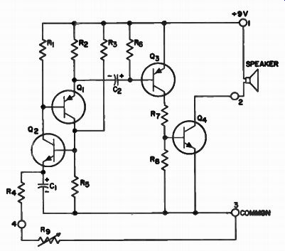
Fig. 112 - Schematic diagram and parts list for the electronic metronome.
-----------------
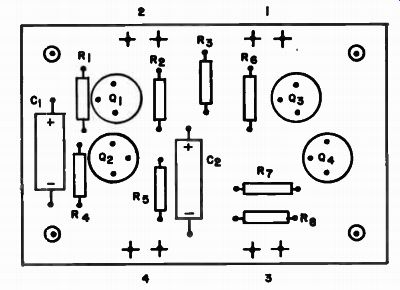
Fig. 113 - Component placement diagram for the electronic metronome.
---------------------
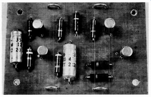
Fig. 114 - Completed circuit board for the electronic metronome.
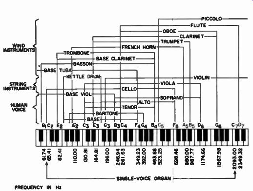
Fig. 115 - Frequency range of the single-voice organ and of instruments within
its range.
Fig. 116 - A suggested enclosure for the single-voice organ.
CIRCUIT NO. 19-SINGLE-VOICE ORGAN
The single-voice organ has a tone that can be varied to simulate the sounds of many musical instruments. Fig. 115 shows the frequency range of the organ and of the instruments within its range. Fig. 116 shows a photograph of a suggested enclosure for the organ.
Circuit Operation
The schematic diagram and parts list for the tone-generator portion of the single-voice organ are shown in Fig. 117. A pulser or clock oscillator is used to form 012 basic tones. The mixer-amplifier arrangement (and parts list) shown in Fig. 118 is used in the audio circuit following the tone generator to charge the character of the tones through the mixing of two signals: a sawtooth wave taken from terminal 9 and a pulse wave taken from terminal 7. Thirteen series-connected resistors are used in the organ to obtain a chromatic scale; five series-connected capacitors are used so that the tone can be keyed up or down two octaves from the middle octave.
Transistors Q3 and Q4 form the basic tone generator; the frequency of this generator is a function of the scale resistor and the octave capacitor selected. The output of the tone generator is frequency modulated through the application of a very-low-frequency sine wave to the base of Q4 and the collector of Q3 ; this sine wave is produced by the twin-T bridge oscillator (which includes Q1 ). (The twin-T bridge oscillator is discussed in detail in the section on General Circuit Considerations.) The capacitors and resistors of the twin-T bridge have been chosen to produce a tremolo signal of about 6 to 7 Hz. Rs controls the frequency or depth of tremolo. The voltage on C7 either aids or opposes the base current that determines the triggering level of the two-transistor switch or tone generator composed of transistors Q3 and Q. When the voltage on C7 aids the base current, the triggering level is reduced and the frequency of oscillation and therefore tremolo increases; when the C7 voltage opposes the current, the frequency and tremolo are decreased.
----------------
Parts List
C1 C2 = 0.22 microfarad, 25 volts or greater, paper
C3 C10 C11 = 0.5 microfarad, 25 volts or greater, paper
Ce = 50 microfarads, 15 volts, electrolytic
C5 = 100 microfarads, 6 volts, electrolytic
Ce C7 = 4 microfarads, 25 volts, electrolytic
CeCe = 0.1 microfarad, 25 volts or greater
0.25 microfarad, 25 volts or greater
0.12 microfarad and 0.005 microfarad in parallel, 25 volts or greater
0.056 microfarad and 0.0068 microfarad in parallel, 25 volts or greater Q1Q2Q4 = transistor, RCA SK3020 Q3 = transistor, RCA SK3005 R1 = 33,000 ohms, 1/2 watt, 10% R2 R3 = 220,000 ohms, 1/2 watt, 10%
C12 = C13 = C14 -=". Re R8= 330,000 ohms, 1/2 watt, 10%
R 5 R18 = 100,000 ohms, 1/2 watt, 10%
R3 = potentiometer, 10,000 ohms, linear taper R7 = 3300 ohms, 1/2 watt 10%
R3 = 270,000 ohms, 1/2 watt, 10%
R10 = 180,000 ohms, 1/2 watt, 10%
R11 R21 R22 = 1000 ohms, 1/2 watt, 10%
R12 = 1500 ohms, 1/2 watt, 10%
R13 = 180 ohms, 1/2 watt, 10%
R1 4 = potentiometer, 1000 ohms, linear taper
R15 = 1200 ohms, 1/2 watt, 10% R16 = 470 ohms, 1/2 watt, 10% R1 7 = 2.2 megohms, 1/2 watt, 10% R19 R20 = 1100 ohms, 1/2 watt, 5% R23 R24 = 9 10 ohms, 1/2 watt, 5% R25 R26 = 820 ohms, 1/2 watt, 10% R2 7 = 750 ohms, 1/2 watt, 5% R28 R29 = 680 ohms, 1/2 watt, 10% R30 = 620 ohms, 1/2 watt, 10% R31 = 10,000 ohms, 1/2 watt, 10%
--------------
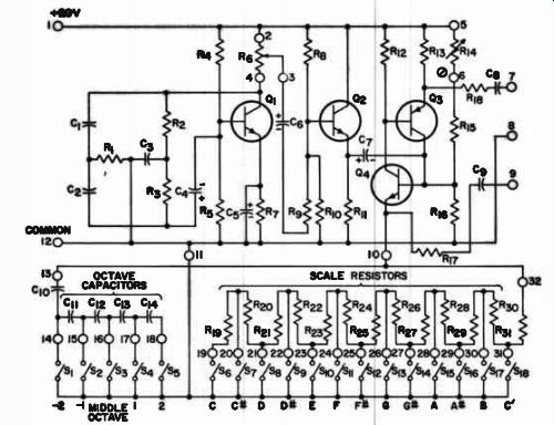
Fig. 117 - Schematic diagram and parts list for the single-voice-organ tone
generator.
----------------
Parts List
C1 = 15 microfarads, 10 volts, electrolytic C2 = 100 microfarads, 6 volts, electrolytic C3 = 50 microfarads, 15 volts, electrolytic Q1 = transistor, RCA SK3020 R1 R3 R3 R3 = 100,000 ohms, 1/2 watt, 10% Rs = potentiometer, 5000 ohms, linear taper R3 = 2.2 megohms, 1/2 watt, 10% R4 = potentiometer, 250,000 ohms, linear taper R7 = potentiometer, 10,000 ohms, linear taper R3 = 330,000 ohms, 1/2 watt, 10% R10 = 12,000 ohms, 1/2 watt, 10% R11 = 3300 ohms, 1/2 watt, 10%
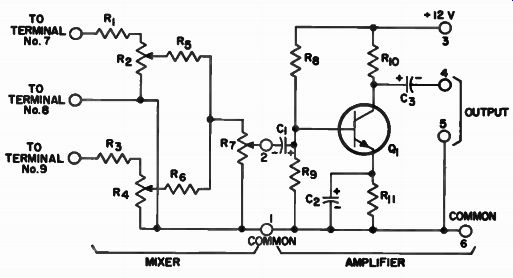
------- Fig. 118 - Schematic diagram and parts list for the single-voice-organ
mixer-amplifier.
----------
The organ is best tuned by comparison with other instruments, such as a piano; R14 is the tuning resistor. Two switches must be depressed to obtain a note: a capacitor switch which selects the octave and a resistor switch which selects the note of the scale. The output of the organ may be fed into a radio, TV, or hi-fi amplifier. The RCA KD2112 Integrated-Circuit Kit Amplifier or the amplifier in Circuit No. 17 of this Manual are also suitable.
The current drain for this circuit (not including the amplifier) is approximately 15 milliamperes.
Fig. 119 (a) - Component placement diagram for amplifier.
Fig. 119 (b)- Component placement diagram for tremolo and tone oscillator.
Fig. 119 (c)- Component placement diagram for resistor board.
Fig. 119(d)- Component placement diagram for capacitor board.
Fig. 120 - Board placement within the suggested enclosure of Fig. 116.
Construction
An easily depressed, normally open, pushbutton switch can be used for the scale and octave switches. The drilling templates for the single-voice organ are shown at the back of this Manual; component placement diagrams for the amplifier, tremolo and tone oscillator, and resistor capacitor boards are shown in Figs. 119 (a) through 119 (d), respectively. Photographs showing board placement within the suggested enclosure are contained in Fig. 120.
CIRCUIT NO. 20-AUTOMOBILE TACHOMETER
The tachometer circuits are used to indicate the speed, in revolutions per minute, of automobile engines with 12 volt electrical systems. Two circuits are described: one for cars with a negative ground, the other for cars with a positive ground.
Circuit Operation
The schematic diagrams for negative-ground and positive-ground auto mobile tachometers are shown in Figs. 121 and 122, respectively. The parts list for both circuits is shown in Fig. 121.
----------- Parts List
C1 = 1 microfarad, 50 volts or greater
C2 = 0.5 microfarad, 50 volts or greater
CRICR1 = silicon rectifier, RCA SK3030
M = milliammeter, 0 to 1 milliampere range (see text)
Q1 = transistor RCA SK3025 for (22 - R1 = R2 = R3 = R4 = R6 = positive ground, RCA SK3020 for negative ground transistor, RCA SK3020 22,000 ohms, 1/2 watt, 10% 220 ohms, 1/2 watt, 10% 1500 ohms, 1/2 watt, 10% 330 ohms, 1/2 watt, 10% potentiometer, 1000 ohms, trimmer type, linear taper
Fig. 121 - Schematic diagram and parts list for the negative-ground tachometer.
Fig. 122 - Schematic diagram for the positive-ground tachometer. ( The parts list for this circuit is shown in Fig. 121).
----------------------
Both tachometer systems operate on the same principle. Pulses from the distributor points are applied to the base of Q1 through terminal No. 1. Q1 turns on and off as the distributor points, open and close; capacitor C1 filters out the "ringing" or voltage oscillations that occur when the points open. Capacitor C2, connected to the collector of Q1, charges through CR1 and R4 when Q1 is off, and discharges through R5, CR2 , and the meter when Q1 is on. Meter deflection is proportional to the rate at which the points open and close.
To make the circuits insensitive to the variations in voltage normally present in an automobile electrical system, transistor Q2 is reverse-biased at the emitter-base junction so that it acts as a zener diode; any 9- or 10-volt, 1/4-watt zener diode may be substituted for Q2.
Trimmer potentiometer R5 is used to calibrate the tachometer. Accuracy of the tachometer circuit can be checked by comparing the revolutions per minute (r/min) reading indicated by this circuit with the reading indicated by a commercial tachometer, such as that used at service stations.
Both positive- and negative-ground tachometer circuits are configured identically; the only difference in the circuits is the substitution of p-n-p for n-p-n transistors and the reversal of the electrolytic capacitors to accommodate the polarity change.
The full-scale r/min reading of the tachometer is determined by the sensitivity of the meter movement. A 1-milliampere movement will have a full scale reading of 8,000 to 10,000 r/min; lower r/min readings require a more sensitive meter movement.
Construction The drilling template for the auto mobile tachometers is shown at the back of this Manual; a component placement diagram and photographs of completed circuit boards for positive and negative ground systems are shown in Figs. 123 and 124 respectively. The component placement dia gram shows the negative ground arrangement. The polarities of the capacitors and rectifiers are reversed for positive ground systems.
Fig. 123 - Component placement diagram for the tachometer.
Fig. 124 - Completed circuit boards for (a) positive-ground and (b) negative-ground tachometers.
CIRCUIT NO. 21-BATTERY CHARGER
The battery charger restores to full strength 6-volt lead-acid storage batteries of the type used in motorcycles and photoflash units. The charging rate of 1 ampere per hour is automatically terminated when the battery is fully charged. This charger may be used for automobile or boat batteries if a slow charging rate is acceptable.
----------------
Parts List
CI = 500 microfarads, 25 volts, RII electrolytic R4 C2 = 100 microfarads, 12 volts, R5 electrolytic R6 C6C4 = 0.01 microfarad, ceramic R7 disc CR 1 through CR6 = silicon rectifier, RCA SK3030 F1 = fuse, 1 ampere, 125 volts I I = lamp, No. 47 Q 1 = transistor, RCA SK3005 Q2 = transistor, RCA SK3020 R1 = 330 ohms, 1/2 watt, 10% R2 adjustable resistor, 5 ohms, 10 watts, 10% T1 =
- 4700 ohms, 1/2 watt, 10%
= 10,000 ohms, 1/2 watt, 10%
= 150 ohms, 1/2 watt, 10%
= 470 ohms, 1/2 watt, 10%
= miniature trimmer control, 5000 ohms, Mallory No. MTC 1 or equivalent SCR1 = silicon controlled rectifier, RCA SK2100 Si = switch, 125 volts, 1 ampere, single-pole, single-throw transformer, primary 117 volts, secondary 25.2 volts at 1 ampere, Stancor No. TP-4 or equivalent.
--------------
Fig. 125 - Schematic diagram and parts list for the battery charger.
---------------
Circuit Operation
The schematic diagram and parts list for the battery charger are shown in Fig. 125. The 120-volt line voltage, stepped down to 25.2 volts by transformer T1 , is rectified by diodes CR1 and CR2 and applied to the anode of SCR1. Diode CR3 prevents capacitor C1, a filter for the gate of SCR1, from discharging through the anode of the SCR when the battery has reached full charge; diode CR4 prevents the battery from discharging through the charging circuit when the circuit has been turned off.
The full-charge condition is deter mined by the voltage-sensing circuit at the right in the circuit schematic. The voltage-sensing circuit, essentially a two-transistor rt generative switch that is triggered into conduction when the voltage across it reaches a level deter mined by the value of R3 and potentiometer R7, turns off SCR, and terminates the charge by making the SCR gate less positive than the cathode.
Potentiometer R7 can be set by the connection of a fully charged battery or a power supply to the charging terminals of the circuit. The battery used should be the type that will normally be under charge; the power supply should be set to 7 volts for lead-acid type batteries. With a fully charged battery in the output, potentiometer R7 is adjusted until the sensing circuit just triggers. Triggering is indicated by extinction of lamp l. After a battery has been fully charged and removed from the circuit, the power to the charger should be momentarily interrupted before a second battery is inserted so that the sensing circuit is reset.
It is important that the charging current not exceed the maximum current rating of diode CR4 . Resistor R2 should be adjusted to 1 ampere or the safe charging rate of the battery, whichever is less. R2 and R7 need not be reset unless the circuit is to be used to charge a battery different from the type normally charged.
Fig. 126 - Component placement diagram for the battery charger.
The secondary of the transformer used in the charger should have a dc resistance of at least 1 ohm. If it does not, a 1-ohm 2-watt resistor should be inserted in series with the secondary.
No special precautions are required if the transformer specified in the parts list is used.
Construction
The drilling template for the battery charger is shown at the back of this Manual, a component placement dia gram and a photograph of a completed circuit board are shown in Figs. 126 and 127, respectively.
Fig. 127 - Completed circuit board for the battery charger.
CIRCUIT NO. 22-ELECTRONIC SIREN
The electronic siren produces a sound like that of a wailing police siren; the frequency of the wail slowly increases and then slowly decreases as a push-button switch is depressed and released.
Circuit Operation
The schematic diagram and parts list for the electronic siren are shown in Fig. 128. When switch S1 is closed, capacitor C1 begins to charge. As it does so, it makes the base of Q1 more and more positive and slowly turns it on. Current conducted through transistor Q1 turns Q2 on (Q1 and Q2 form a direct-coupled amplifier). Part of the output from Q2 is applied to the input of Q1 through capacitor C2 and provides the regenerative feedback that causes the circuit to oscillate. When switch S1 is opened, C1 discharges through R2 and the base of Q1. The "wailing rate" of the siren can be changed by substituting different values of B1 and C1. An increase in the value of R1 or C1 lengthens the rate at which the frequency of oscillation increases.
Because battery drain with switch Si open is only about 400 microamperes, a power switch is not considered necessary. However, such a switch will 9V add to battery life.
Fig. 128 - Schematic diagram and parts list for the electronic siren.
Fig. 129 - Component placement diagram for the electronic siren.
Fig. 130 - Completed circuit board for the electronic siren.
Construction
The drilling template for the electronic siren is shown at the back of this Manual; a component placement dia gram and a photograph of a completed circuit board are shown in Figs. 129 and 130, respectively.
Parts List
C1 = 50 microfarads, 12 volts, electrolytic
C2 = 0.018 microfarad, 25 volts or greater Q" = transistor, RCA SK3020
Q2 = transistor, RCA SK3005
R1 = 27,000 ohms, 1/2 watt, 10%
R2 = 68,000 ohms, 1/2 watt, 10%
R3 = 56,000 ohms, 1/2 watt, 10%
R4 = 470 ohms, 1/2 watt, 10%
S1 = switch, any single-pole push button type
Speaker = 3.2-ohms or 8-ohms
CIRCUIT NO. 23-ELECTRONIC SLOT MACHINE
Fig. 131 - A suggested enclosure for the electronic slot machine.
The completed electronic slot machine game resembles, functionally, the well-known Las Vegas slot machine except that a push-button replaces the lever and three vertical columns of lights replace the spinning wheels.
Each light corresponds to a lemon, cherry, or other symbol found in the conventional machine. Instead of paying off in coin, the electronic slot machine indicates a score through one of six scoring lamps on its face. A suggested enclosure for the slot machine is shown in Fig. 131.
To operate the slot machine, a player depresses the push-button switch momentarily. Each column of lights then starts to flash in sequence; the duration of flashing changes each time the game is played. The maximum time for game completion is approximately four seconds. When the flashing stops, one of the lamps remains lit in each column; the combination of the three lighted lamps is completely random and determines the score. When no score lamp lights, the score is zero.
The electronic slot machine circuit makes use of the digital circuits described in the section on General Circuit Considerations: the NAND and NOR gates, the flip-flop, and the shift register. For this reason the slot machine circuit represents an excellent means of gaining practical experience in digital circuitry.
Fig. 132 - Block diagram of the electronic slot machine.
Fig. 133 - Interconnection diagram for the running and stop oscillators, flip-flops, and NA ND gates A, B. and C.
Fig. 134
------------------------ Parts List
Cr1 through CR9 = silicon rectifier, 1 through 16 = lamp No. 1488 RCA SK3030
-------------
Fig. 135 - Interconnection diagram for the score gate circuits (NOR gates) and the score lamps.
----------
Parts List
Running Oscillator (1 req'd)
C1 = 2 microfarads, 15 volts, electrolytic
Q1 = transistor, RCA SK3005
Q2 = transistor, RCA SK3020
R1 = 1500 ohms, 1/2 watt, 10%
R2 = 47 ohms, 1/2 watt, 10%
R3 = 1000 ohms, 1/2 watt, 10%
R4 = 15,000 ohms, 1/2 watt, 10%
R5 = 4700 ohms, 1/2 watt,10%
Stop Oscillator (3 req'd)
C1 100 microfarads, 15 volts, electrolytic
Q1 = transistor, RCA SK3005
Q2 = transistor, RCA SK3020
R1 = 1000 ohms, 1/2 watt, 10%
R2 = 68 ohms, 1/2 watt, 10%
R3 = 1000 ohms, 1/2 watt, 10%
R4 = 27,000 ohms, 33,000 ohms, 39,000 ohms, one in each of 3 oscillators
R5 470 ohms, 1/2 watt, 10%
Fig. 136 - Schematic diagram and parts list for the running and stop oscillators.
--------------
Circuit Operation
The electronic slot-machine circuit consists of a series of building blocks; each block is constructed on a circuit board and interconnected as shown in the diagram of Fig. 132. Detailed inter connections for various portions of the circuit are given in Figs. 133, 134, and 135. Detailed schematics for each building block are shown in Figs. 136 through 141. The parts list for each circuit is shown with the schematic.
-----------------------
Parts List
C1 C2 = 560 picofarads, 25 volts or greater
C3 = 0.01 microfarad, 25 volts or greater
CR 1 = silicon rectifier, type 1N270
Q1 Q2 = transistor, RCA SK3020
R1 R2 = 1500 ohms, 1/2 watt, 10%
R3 R. R5 = 10,000 ohms, 1/2 watt, 10%
R6 R7 = 6800 ohms, 1/2 watt, 10%
Fig. 137 - Schematic diagram and parts list for the flip-flops.
-----------------
Parts List
C7 = 0.1 microfarad, 25 volts or greater
Q1 Q2 = transistor, RCA SK3020
R1 = 1000 ohms, 1/2 watt, 10%
R2R3 = 10,000 ohms, 1/2 watt, 10%
Fig. 138 - Schematic diagram and parts list for the NAND gates (A, B, C).
----------------------
Parts List
CR 1 CR2 = silicon rectifier, RCA SK3030 Q1Q3 = transistor, RCA SK3005 Q2 = transistor, RCA SK3010 R7 through R6 = 4700 ohms, 1/2 watt, 10% R2 R3 R4 = 4700 ohms, 1/2 watt,
10% R7 = 3900 ohms, 1/2 watt, 10% Re R9 = 180 ohms, 1/2 watt, 10%
Fig. 139 - Schematic diagram and parts list for the NOR gate circuit and lamp driver for score 2.
------------------
Parts List
Q1 = transistor, RCA SK3010
Q2 = transistor, RCA SK3005
Rilt 2 R3 R4 = 4700 ohms, 1/2 watt, 10%
R5 = 270 ohms, 1/2 watt, 10%
R8 = 150 ohms, 1/2 watt, 10%
Fig. 140 - Schematic diagram and parts list for the NOR gate circuits and lamp drivers for scores 10 through 100.
----------------------
Parts List
C1 = 2000 microfarads, 15 volts, electrolytic
CR1 through CR7 - silicon rectifier, RCA SK3030
CR8 = zener diode, 13 volts, 1 watt
F1 = fuse, 1 ampere, 3AG
Q1 = transistor, RCA SK3005
Q2 = transistor, RCA SK3009
R1 = 1800 ohms, 1/2 watt, 10%
R2 = R3 = R4 = S1 = T1 = 68 ohms, 1/2 watt, 10% 470 ohms, 1/2 watt, 10% 100 ohms, 25 watts, adjustable toggle switch, single-pole single throw transformer, primary 117 volts, secondary 25 volts at 1 ampere, Stancor No. P6469 or equivalent
---------------
Fig. 141 - Schematic diagram and parts list for the slot machine power supply.
---------------------------
When power is applied to the circuit, the "running" and "stop" oscillators begin pulsing. The running oscillator pulses at a very rapid rate; the stop oscillators all pulse at a slightly different rate but produce a pulse approximately once every four seconds. The stop and running oscillators continue to pulse as long as power is on.
When the push-button switch shown in Fig. 133 is depressed, the flip flop circuits assume the output state; their outputs and the pulses from the running oscillator are applied to the gate circuits. Gate circuits with both inputs (running oscillator and flip-flop) satisfied provide an output each time the running oscillator pulses; this output is applied to the shift register which advances the lighted lamp in each column with each pulse.
At this point in the circuit operation, all three columns of lamps are flashing. The score lamps may also flash momentarily at this time as score gate-circuit output conditions are momentarily satisfied. The flashing of the lamps in each column continues until the stop oscillator associated with a particular column pulses once. This pulse can occur, as explained above, at any time up to four seconds after the push-button switch is released. The pulse sets the flip-flop to the no-output state and cuts off the input to the gate.
Because the conditions for gate output are not satisfied, running oscillator pulses are not transmitted to the shift register.
The shift-register outputs that light the lamps in each column are also applied to the input of the score gates.
When the final lighted-lamp combination matches one of the preset scoring conditions, a scoring lamp lights.
Table V shows the lamp combinations and associated suggested point values.
---------------
Any in first row with:
Table V. Electronic Slot-Machine Scores
Lamps Lighted Suggested Score
All first row 100
All second row 18
All third row 14
All fourth row 10
Any two fifth row lamps 5
Any two in second row 18
Any two in third row 14
Any two in fourth row 10
Any one in fifth row 2
None of above
------------------------
Detailed Circuit Considerations
Both the running and stop oscillators shown in Fig. 136 are basically the same circuits, astable pulsers; they differ only in the values of the timing components. The timing capacitor C1 in the stop oscillator is large compared to the timing capacitor C1 in the running oscillator. The charging resistors, R4, in the stop oscillators must differ slightly to insure a complete random action in the score lamps.
The astable pulser description in the section on General Circuit Considerations contains a statement to the effect that the regenerative switch portion of the pulser conducts immediately with the application of power. The pulse conducted consists of a stop pulse in the negative direction; this pulse is applied to the flip-flop circuits which are in the no-output state when power is applied to the circuit. A momentary depression of the push-button switch places the flip-flops in the output state.
The flip-flop circuit used in the electronic slot machine is the same as that described in the section on General Circuit Considerations except that a number of unnecessary components have been omitted. Fig. 137 shows the modified basic flip-flop.
The power supply in Fig. 141 is a modification of the fixed series supply, Circuit No. 1 (a). The slot machine lamps receive full-wave rectified dc through diodes CR1 and CR2. Diode CR3 keeps C7 , the filtering capacitor, from discharging back through the lamp circuit, a condition that would increase the ripple voltage output of the supply. Diode CR 3 also permits the use of a value fo - C1 that is smaller than would otherwise be possible.
Diodes CR, through CR7 and resistors R3 and R4 make available the additional voltage values required by the slot-machine circuit. R4 should be adjusted so that there are 5.6 volts across the wiper arm (adjustable tap) and the common terminal.
Construction Each circuit of the same type in the electronic slot machine uses the same board although the value of one or two of the components may differ. The boards for the same circuit type may be cut and drilled simultaneously; drilling templates are shown at the back of the Manual. Component placement diagrams and photographs of completed circuit boards are shown in Figs. 142 through 146. The list below indicates how many of each circuit type must be constructed.
The push-button switch used to activate the slot-machine game can be any normally closed type.
The completed slot machine shown in Fig. 131 represents but one method of construction. Many other methods are possible and depend on the material used for the chassis, the lamp socket chosen, etc. If desired, a care fully made replica of an actual slot machine can be used to house the electronic counterpart.
----------------
Circuit Modules Required
Number Required Schematic
Running Oscillator Stop Oscillator Flip-Flop Nand Gates Score Gate (Lamp 16)
Score Gate (Lamps 1 through 16 )
Power Supply Shift Register
1 3 3 3 1 5 1 3
Fig. 136 Fig. 136 Fig. 137 Fig. 138
Fig. 139 Fig. 140 Fig. 141 Circuit No. 2
-----------------
Fig. 142( a)- Component placement diagram for the running and stop oscillators
Fig. 142(6)- Completed circuit board for running and stop oscillators.
-----------------
Fig 143(a)- Component placement diagram for the flip-flop.
Fig. 143( b )- Completed circuit board for the flip-flop.
--------------------
Fig. 144(a)- Component placement diagram for the NAND gates (A, B, C). Fig. 144(b)- Completed circuit board for the NA ND gates (A, B. C).
------------------
Fig. 145(a)- Component placement diagram for the NOR gate and lamp driver for score 2.
Fig. 145(6)- Completed circuit board for the NOR gate and lamp driver for score 2.
-----------------
Fig. 146(a)- Component placement diagram for the NOR gate and lamp drivers for scores 10 through 100.
Fig. 146( b) - Completed circuit board for the NOR gate and lamp drivers for scores I() through 100.
-----------------
CIRCUIT NO. 24 - ELECTRONIC DIE
The electronic die can display any of the dot patterns that exist on the faces of a conventional die. When the push-button switch is depressed the display lights flash randomly for a few seconds, then stop in a combination representing a number from 1 through 6. If a pair of dice is needed, the single die can be operated twice or a second die can be built; one power supply is sufficient to power a pair of electronic dice. A suggested enclosure for the electronic dice is shown in Fig. 147.
Fig. 147- A suggested enclosure for the electronic die circuit.
Circuit Operation
The schematic diagrams and parts lists for the electronic die are shown in Figs. 148 and 149.
When push-button switch S1 (shown in Fig. 148) is depressed, capacitor C2 charges rapidly to nearly 12 volts; the resultant current through R6 is sufficient to start pulser oscillation. The output pulses from the pulser key the shift register (Circuit No. 2) which is connected as a ring counter; i.e., each stage follows the sequence as if placed around a circle or ring. Stage one in the ring generates the number 1, stage two generates the number 2, and so on.
Each pulse input to the ring counter advances the counter one stage.
When the push-button switch S1 is released, C2 discharges slowly through R5 and the pulsation rate decreases until oscillation stops. When oscillation has stopped, the arrangement of illuminated lamps on the face of the electronic die remains fixed. The nine diode "OR" gate shown in Fig. 149 gates the output of the shift register to the lamp drivers and assures that the lamps light in proper sequence.
-------------
Parts List
C1 = 1 microfarad, 25 volts, electrolytic C2 = 500 microfarads, 25 volts, electrolytic C3 = 100 microfarads, 6 volts, electrolytic C4 Cg through C11 = 0.05 microfarad, 25 volts or greater, ceramic C5 = 10 microfarads, 25 volts, electrolytic CR 1 through CR6 = silicon rectifier, type 1N270 CR, CR 8 = silicon rectifier, RCA SK3030 Q1Q 4 through Q9 = transistors, RCA SK3005 Q2 = transistor, RCA SK3020 Q3 Q io through Q15 .= transistor, RCA SK3010 R1 = 1500 ohms, 1/2 watt, 10% R2 R3 = 47 ohms, 1/2 watt, 10% R3 = 27,000 ohms, 1/2 watt, 10% R, R12 through R18 = 1000 ohms, 1/2 watt, 10% R5 = 3300 ohms, 1/2 watt, 10% R3 = 15 ohms, 1/2 watt, 10% R9 = 5600 ohms, 1/2 watt, 10% R10 R11 = 470 ohms, 1/2 watt, 10% R17 through R22 = 270 ohms, 1/2 watt, 10%
-------
Fig. 148 - Schematic diagram and parts list for the digital pulser and six-stage shift register.
Fig. 150 shows a modification that must be made to the supply (universal series power supply, circuit No. 1(a)) used to power the electronic die. The modification consists of the addition of diode CR, between the cathodes of the rectifiers and the filter capacitor.
----------
CR1 through CR9 = silicon' rectifier, type 1N27011 through 17 = any 12-volt lamp drawing 150 milliamperes or less Q1 through Q7 = transistor, RCA SK3020 R1 through Re = 1200 ohms, 1/2 watt, 10% R7 through R13 = 680 ohms, 1/2 watt, 10%
Fig. 149 - Schematic diagram and parts list for the indicator-lamp gate and driver circuit.
----
Fig. 150 - Universal series power supply (Circuit No. 1(a)) modified to suit power requirements of the electronic die.
-----------
Terminal 14 of the die circuit is connected as shown. The electronic-die display lamps receive full-wave rectified current through the rectifying diodes. CR. in Fig. 150 prevents the filter capacitor from discharging back through the diodes and into the lamp circuit, a condition that would increase the ripple-voltage output of the supply.
The presence of CR, also makes possible use of a C1 with a smaller electrical capacitance than would otherwise be suitable.
Construction The design of the electronic die incorporates a power supply and three basic modules: the digital pulser, the shift register, and the lamp module.
Drilling templates for these circuits are shown at the back of the Manual; photographs of the completed circuit boards and component placement diagrams are shown in Figs. 151 and 152. The arrangement of components is not critical; a circuit layout different from that suggested may be used.
CIRCUIT NO. 25 -METAL DETECTOR
This circuit can be used to locate buried metal objects, such as water or gas pipes, and metal objects such as coins lost in grass, loose earth, or sand.
When no metal is near, a steady tone is heard in the headphones connected to the metal detector. When metal is present, the tone either changes or cuts off completely, depending on how the detector is set. The detector locates metal; it does not determine the size or the depth below the surface of that metal.
Fig. 151(a) - Completed circuit board for the digital pulser and six-stage shift register.
Fig. 151(b)
Circuit Operation
The schematic diagram and parts list for the metal detector are shown in Fig. 153. The circuit consists of two oscillators. The first oscillator, which includes Q1, operates at approximately 300 kHz, a frequency determined by inductor L1 and capacitor C2. The second oscillator, which includes Q2, operates at a frequency determined by C11 and the search coil. L1 is adjusted so that its frequency of oscillation is close to that of the search coil. (The procedure for adjusting L1 is described below.) The output of the oscillators is fed into a product detector through C5 and C6. The product detector produces an audio signal when there is a difference in frequency between the outputs of the two oscillators. A difference in frequency occurs when the search coil is brought close to a metal object and its inductance, and therefore its frequency of oscillation, is changed. The audio output from the product detector is applied to the base of Q3, which amplifies the signal to an audible level.
Adjustments and Operation
With the circuit energized, inductance L1 is adjusted until a tone is heard in the headphones. Variable capacitor Cn, a fine-tuning control, is used as an aid in achieving maximum sensitivity, a condition signaled by a "motorboating" or "putt-putt" sound in the headphones. The detector is then ready for use. As the search coil is passed slowly over the ground and as close to the ground as possible, a change of tone or the cessation of tone indicates the presence of metal. Damp ground may also cause the tone to change, and may necessitate readjustment of the detector with the search coil held near the ground. The current drain for this circuit is 3 milliamperes.
Fig. 152(a)- Completed circuit board for the indicator-lamp gate and driver circuit.
Fig. 152(b; - Component placement diagram for the indicator-lamp gate and driver circuit.
------------
Parts List
C1 C7 C1 4 = 0.01 microfarad, 25 volts or greater C: - 1800 picofarads, 25 volts or greater C3 CI: = 3900 picofarads, 25 volts or greater C4 C: CI: = 0.001 microfarad, 25 volts or greater Cs Ce = 0.004 microfarad, 25 volts or greater C: = 680 microfarads, 25 volts or greater C1 1 = 20 picofarads, variable type, Hammarlund No. MAC-20 or equivalent C1 2 = 0.02 microfarad, 25 volts or greater C1 : = 50 microfarads, 6 volts, electrolytic C16 = 0.1 microfarad, 25 volts or greater CR 1 CR 2 = silicon rectifier, type 1N34A Re: = 22,000 ohms, 1/2 watt, 10% RA: = 47000 ohms, 1/2 watt, 10% Res = 2200 ohms, 1/2 watt, 10% R4 R7 = 1 megohm, 1/2 watt, 10% 3 = 68,000 ohms, 1/2 watt, 10% R1 : = 10,000 ohms, 1/2 watt, 10% R11 = 91,000 ohms, 1/2 watt, 10% R1 2 = 680 ohms, 1/2 watt, 10% R13 = 6800 ohms, 1/2 watt, 10% Q1Q2Q3 = transistor, RCA SK3020 L1 = 50 to 140 micro-henries, adjustable Copper tubing: 1/4-inch diameter, 3.14 feet (enough for loop of 1-foot diameter)
No. 24 enameled copper wire: about 40 feet (enough for 12 turns of 1-foot diameter and connections)
Coaxial cable: about 3 feet (exact amount depends on length of handle)
Earphones = 200 ohms
Fig. 153 - Schematic diagram and parts list for the metal detector.
---------------
Construction
The most critical member of the metal detector is the search coil. The coil consists of 12 turns of No. 24 enameled wire enclosed in a 1-foot diameter loop of 1/4-inch copper tubing. The ends of the loop should be about 2 inches apart at the beginning of search-coil construction and should not be electrically connected. To form the turns within the tubing, one end of the No. 24 wire is fed into one end of the copper tubing and pushed through until it emerges from the other end.
The end of the wire that has just emerged is reinserted into the tubing and pushed through as before. This process is repeated until there are 12 turns of wire within the loop. When this task is completed, the loop must be closed so that there is a space of only 1/4 inch between the ends. The loop can be closed by pulling on the ends of the wire within the loop. One end of the wire and the braided conductor of the coaxial cable should then be connected to one end of the copper loop. The other end of the wire should be connected to the center wire of the coaxial cable. Fig. 154 shows a finished search coil A handle must then be connected to the search coil as shown in Fig. 154.
Metal fasteners should not be used in the area of the coil. The circuit portion of the detector should be mounted as far as possible from the search coil; a good location is on the upper part of the handle. Layout of the detector circuit is not critical; however, it should be mounted in a metal box as shown in Fig. 155.
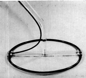
Fig. 154 - A completed search coil with handle attached.
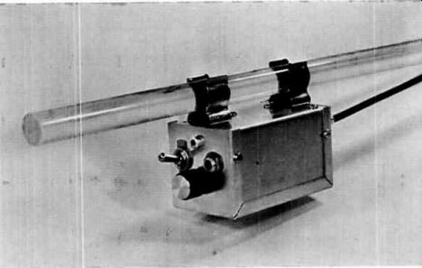
Fig. 155 - A suggested enclosure for the metal-detector circuit.
CIRCUIT NO. 26 -- DIP/WAVE METER
One of the most useful instruments available to the electronics experimenter working in rf is the MOS field effect transistor dip/wave meter. A photograph of the unit is shown in Fig. 156. The meter is essentially an oscillator that can be used to measure resonant frequencies. With the power switch OFF the meter becomes an absorption type wavemeter that measures the resonant frequency of energized rf circuits; with the power switch ON, the meter measures the resonant frequency of unenergized rf circuits. Then, if the inductance of the circuit is known, the capacitance can be calculated; if the capacitance is known the inductance can be calculated.
In operation, the coil of the meter is placed close to the tuned circuit to be measured. Capacitor C1 is then tuned until a movement of the meter needle is observed. If the dip/wave meter is being used to measure an energized circuit, the needle will jump upward slightly when the frequency of the meter oscillator matches that of the LC circuit being measured. If the dip/wave meter is being used to measure the frequency of an unenergized LC circuit, the needle will dip sharply at the point of resonance. If the meter gives no indication a different meter coil should be tried.
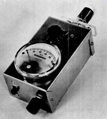
Fig. 156 - A suggested method of assembling the dip/wave meter Circuit Operation
Fig. 157 shows the schematic dia gram and parts list of the dip/wave meter, which is essentially an MOS field-effect-transistor oscillator.
Oscillator feedback is provided by return of the source to a tap on the coil; transistor operating bias is obtained through the bypassed source resistor R2 . Oscillator rf voltage is rectified by diode CR1 and measured with the microammeter M. Potentiometer R3 adjusts the supply voltage to the oscillator and the intensity of oscillations or sensitivity of the dip/wave meter. R3 also controls the meter reading. C1 sets the frequency of the dip/wave meter.
Care should be taken when the dip/wave meter is being operated as a wave meter not to overdrive the circuit to the extent that the field-effect transistor is subjected to greater gate signals than it is capable of accommodating. This condition is encountered when the meter is deflected beyond full scale.
Power is supplied to the dip/wave meter by a 9-volt transistor battery.
The current drain for this circuit is 2 milliamperes maximum.
------------------
Parts List
c = C2 = C3 =
Battery = 9-volt
transistor type, RCA VS323 or equivalent variable capacitor, 50 picofarads; Hammarlund HF-50 or equivalent
0.01 micro-farad, 50 volts or greater, ceramic
0.001 microfarad, 50 volts or greater, ceramic
C4 = 0.01 microfarad, 50 volts or greater, ceramic
C5 = 0.01 microfarad, 50 volts or greater, ceramic
CR 1 = silicon rectifier, type 1N914
L1 = see Table V
M = microammeter, 0 to 100 microamperes
MOS field-effect transistor, type 3N128
R1 = 47,000 ohms, 1/2 watt, 10%
R2 = 1000 ohms, 1/2 watt, 10%
R3 = potentiometer, 10,000 ohms, linear taper
R4 = 6800 ohms, 1/2 watt, 10%
S1 = switch, double-pole, double throw
Q1 =
--------------
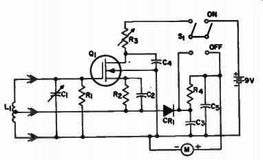
Fig. 157 - Schematic diagram and parts list for the dip/ wave meter.
------------
Construction
The coils used with the dip/wave meter are wound on polyethylene tubing and glued with acrylic cement to a polyethylene bar containing three banana plugs. The ends of the coil are connected to the two end plugs; the center tap is connected to the center plug. The coil terminals on the dip/wave meter should be recessed so that they cannot be short circuited, a condition that could cause damage to the MOS transistor. A table of typical values is given in Table VI. Fig. 158 shows a number of completed coils.
------------
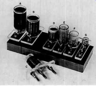
Fig. 158 – Dip / wave meter coils. The coils are described in detail in Table
VI.
Table VI.
Dip/Wave Meter Typical Coil Characteristics
*Coils A to D close wound on polyethylene forms; E and F space wound on polyethylene forms; G self supporting. The coils are pictured in Fig. 158.
+ Enameled
a Tin Plated
---------------------
CIRCUIT NO. 27-VARIABLE - FREQUENCY OSCILLATOR
The variable-frequency oscillator (vfo) circuit can be used with a fixed or mobile radio-amateur transmitter and is capable of excellent performance with minimum frequency drift at frequencies up to and including vhf. Operating potentials can he obtained directly from a 12-volt source, such as an automobile battery, dry battery, or low-voltage power supply (Circuit No. 1(a)). Fig. 159 shows a photograph of the vfo.
Circuit Operation
The schematic diagram and parts list for the variable-frequency oscillator are shown in Fig. 160. This oscillator is basically of the Colpitts type; each of the turning ranges shown in Table VII is band spread over almost all of the turning dial for accurate calibration and resettability. The effect of changes in transistor element capacitance is minimized by use of a voltage divider consisting of C4, C5, C6, with the transistor connected across C5 and C6. The use of fairly large values for C5 and C6 almost completely suppresses the effect of transistor capacitance. A radio-frequency choke L2 provides the needed low IR drop for the source current of the MOS transistor.
Because the MOS transistor by itself will not provide rectified gate current, a silicon diode, CR1 , is used in the gate circuit. This diode contributes considerably to the frequency stability of the oscillator by providing automatic bias which tends to compensate for changes in output load and supply voltage.
The vfo output is taken from the source of the MOS transistor through a two-stage negative-feedback amplifier which performs two basic functions:
1. It greatly minimizes the effect on the oscillator of a change in output conditions.
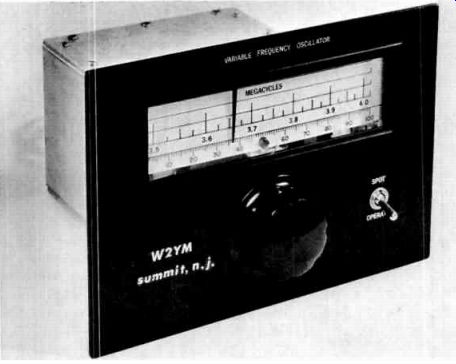
Fig. 159 - Suggested enclosure for the variable-frequency oscillator.
--------------
Parts List
C1 = variable capacitor, high-quality, double-bearing type, Miller 23100 or 23050 or equivalent (See Table VII for value)
Cs= 25-picofarad air-type trimmer capacitor; Hammarlund APC-25 or equivalent C8
C4 C5 Cs = silver mica capacitors, 300 volts (See Table VII for values)
C7 - 2200 picofarads, 300 volts, silver mica
0.05 picofarad, 50 volts or greater, ceramic disc
Co = 0.1 picofarad, 50 volts or greater, ceramic disc
C10 C11 = 1500 picofarads, 500 volts, feedthrough type C is = 0.025 microfarad,50 volts or greater, ceramic disc
CS = ENCLOSURE CR1 = silicon rectifier, type 1N914 J i = coaxial connector, chassis-mount vhf type
L1 = (See Table VII for values)
L5 = 2.5 millihenries, miniature rf choke, iron core, Millen J300 2500 or equivalent
Q1 = MOS field effect transistor, type 3N128
Q5 = transistor, RCA 40245
Q8 = transistor, RCA SK3020 R = 22,000 ohms, 1/2 watt, 10%
R2 = 12,000 to 47,000 ohms, 1/2 watt, 10%; select for 2-volt peak output
R8 = 12,000 ohms, 1/2 watt, 10%
R3 = 820 ohms, 1/2 watt, 10%
R5 = 47,000 ohms, 1/2 watt, 10%
R3 = 240 ohms, 1/2 watt, 10%
---------------
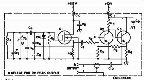
Fig. 160 - Schematic diagram and parts list for the variable-frequency oscillator.
-------------
2. It provides a convenient means of adjusting the output voltage of the vfo by changing the value of R2 . The use of silver-mica capacitors assures a fairly stable temperature characteristic.
Power is supplied to the vfo through two 1500-picofarad feedthrough capacitors. The 10- and 6.8-volt power levels required can be obtained from a modified universal-series supply. The modification is shown in Fig. 161; the Universal-series supply is described in Circuit No. 1 (a).
Construction
The complete vfo should be housed in a 4- by 5- by 6-inch aluminum utility box. The MOS transistor oscillator components of the vfo must be installed in the box with maximum rigidity. This installation can be accomplished by mounting all oscillator components (less the tuned circuits) on a terminal strip (H.H. Smith No. 1070 or equivalent); the two-stage ...
-------------------
Table VII.
Tuned-Circuit Data for the VFO
CR1 = zener diode, 6 8 volts, 1 watt
R1 = 180 ohms, 1/2 watt, 10%
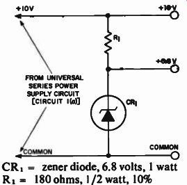
Fig. 161 - Universal-series-power-supply modification for use with the variable
frequency oscillator circuit.
----------------------
... amplifier can be mounted on a similar strip. This arrangement is shown in Fig. 162. The lower strip in the figure supports the oscillator components; the MOS transistor projects downward from the center of the strip. The upper strip is for the two-stage amplifier; the transistor project upward on either side of the mounting screw. The short length of coaxial cable runs to the connector on the rear of the aluminum box. The silver-mica capacitors which form part of the tuned circuit must be mounted in such a way that there is no possibility of motion. A photograph of the tuned circuit assembly is shown in Fig 163. In the figure, the tuned circuit is supported by a bent aluminum sheet extending from the front to the rear of the 4- by 5- by 6-inch box. The trimmer capacitor, C2, is mounted on the rear wall, as are the coaxial output connector and feedthrough bypass capacitors for the power leads.
A single-pole double-throw switch can be connected in the circuit so that in one position only the vfo power supply is turned on. With the switch in the other position, power is supplied through the main transmitter supply and the vfo is activated by the transmit/receive switch in the transmitter.
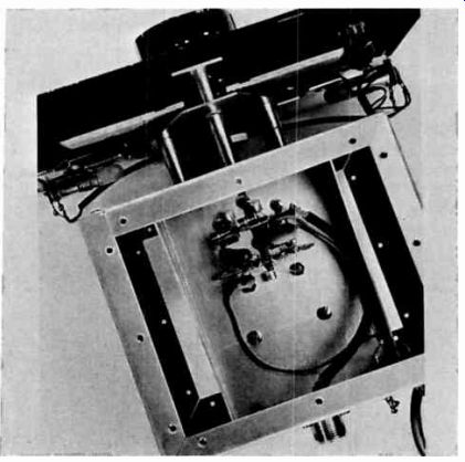
Fig. 162 - Suggested mounting of oscillator and two-stage amplifier components.
Fig. 163 - Suggested tuned circuit assembly.
CIRCUIT NO. 28-VFO CALIBRATOR
In the vfo calibrator, harmonics of a secondary-standard 100-kHz crystal oscillator are beat with the fundamental, or harmonics, of an external vfo to provide audible signals at definite frequencies across the dial. For example, if this unit is used with a 5.0-to-5.5 MHz vfo, the 100-kHz calibration points are the strongest by far. however, the 50-kHz points are also perceptible and, if proper care is exercised, the 33-, 25-, and 20-kHz points can be detected a; well. In practice, the calibrator is permanently connected to the rf line between the vfo and the transmitter. A suggested enclosure for the vfo calibrator is shown in Fig. 164.
Fig. 164 - A suggested enclosure for the vfo calibrator.
Circuit Operation
The schematic: diagram and parts list for the vfo calibrator are shown in Fig. 165. The 100-kHz oscillator, Q3 , is of the tuned-collector type, with the crystal Y I inserted in the base feedback circuit. The 25-picofarad padder capacitor, C4 (crystal adjust), is connected in series with the crystal so that oscillation can be adjusted to exactly 100 kHz. Capacitors C7 and C8 are used as a voltage divider to reduce the coupling to the input of the two-stage wave-shaping amplifier, Q4 and Q5, and thus prevent loading of the secondary-standard oscillator. The two-stage wave-shaping amplifier provides the following advantages:
1. It prevents any reflection of the output load from affecting the frequency of the 100-kHz secondary standard oscillator.
2. It shapes the output wave so that the harmonics are of greater strength.
The output of the two-stage wave- ...
--------------
Parts List
C1 = 25 picofarads, adjustable padder type, air dielectric, Hammar lund APC-25 or equivalent C2C3C19 = 0.1 microfarad; 25 volts or greater, ceramic
= 470 picofarads, 500 volts, silver mica C5 = 1200 picofarads, 500 volts, silver-mica C8 = 0.25 microfarad, 25 volts or greater, paper C7C 77 = 50 microfarads, 6 volts, electrolytic C8 = 0.001 microfarad, 25 volts or greater, ceramic C9 = 100 picofarads, 25 volts or greater, ceramic
C12 C15 = 0.0022 microfarad, 25 volts or greater, ceramic
C13 = 500 microfarads, 15 volts, electrolytic
C14 = 22 picofarads, 25 volts or greater, ceramic
Cie = 0.05 microfarad, 25 volts or greater, ceramic
C 17 = 0.03 microfarad, 25 volts or greater, ceramic
CR 1 CR : = silver rectifier, type 1N34A
L1 = RF choke, 10 millihenries, Miller 70F-102A1 or equivalent
Q1Q2Q4Q5 Q6 = transistor, RCA SK3020
Q3 = transistor, RCA SK3005 R1 R4 = 82,000 ohms, 1/2 watt, 10% R2 = 22,000 ohms, 1/2 watt, 10% R3 = 4 700 ohms, 1/2 watt, 10% R5 R12 R13 = 47,000 ohms, 1/2 watt, 10% R3 = 120,000 ohms, 1/2 watt, 10% R7 R9 Ri4 R15 = 2700 ohms, 1/2 watt, 10% R3 RIO = 470 ohms, 1/2 watt, 10% R1 1 = 6800 ohms, 1/2 watt, 10% R16 = 330 ohms, 1/2 watt, 10% R17 R1 8 R21 = 10,000 ohms, 1/2 watt, 10% R1 g R20 = 1 megohm, 1/2 watt, 10% R22 = 68,000 ohms, 1/2 watt, 10% Y1 = crystal, Valpey-Fisher type VR 13 or equivalent (calibrated at 100 kHz, service mode)
Earphones = 600 ohms or more
----- Fig. 165 - Schematic diagram and parts list for the vio calibrator.
---------
... shaping amplifier is connected to one input of a two-diode product detector, CR4 and CR5 , and the vfo to be calibrated is connected to the other input.
The wave-shaping amplifier output is connected in such a way that the unit can be used as a conventional 100-kHz crystal calibrator. The values of the components shown in the parts list have been chosen for a vfo signal of 2 to 3 volts. For larger signals, the 22 picofarad capacitor C17 must be replaced with some type of capacitance or resistive attenuator A three-stage audio amplifier consisting of Qs, Q7, and Qs is used to amplify the extremely low audio output of the two-diode product detector to a comfortable head-phone level.
The crystal socket and the air capacitor used for setting the frequency should be mounted on a small piece of aluminum and attached to one end of the circuit board. If a metal enclosure is used, the circuit board should be separated from it by at least 3/8 of an inch. RF connections to the vfo and transmitter can be made through standard coaxial connectors.
Adjustments and Operation
The adjustment of the 100-kHz secondary-standard oscillator to precisely 100-kHz is easily accomplished by comparison of its harmonic with that of the primary standard, WWV*. For the best beat signal, the 100-kHz output of the calibrator should be loosely coupled to the antenna of the receiver tuned to WWV. Capacitor C4 should then be adjusted through the crystal-adjustment hole until a zero beat exists between the secondary ...
*The Radio Amateur's Handbook.
American Radio Relay League, Newington, Conn.
... standard and WWV. It would be well to wait for the quiet period of WWV's transmission (when there is no 440-Hz modulation) to be absolutely certain that the secondary standard is beating with the carrier and not with one of the sidebands.
The calibrator is very easy to use. It is inserted in the rf line of the vfo by connecting the vfo to the input coaxial connector and the transmitter to the output connector. When power is applied to the unit, a slight hissing noise should be heard in the earphones.
This noise indicates that the audio amplifier is active. At, or near, the even 100-kHz points on the vfo, low beat notes should be heard. Calibration of the dial can then be performed by zero-beating the vfo at those points.
Lower-volume beats may be heard at the 50-kHz points on the dial, and in most cases it is also possible to hear the 33-, 25-, and 20-kHz beats, especially if the fundamental operating frequency of the vfo is below 5 MHz.
With many of today's amateur radio receivers designed solely for hamband reception, the vfo calibrator is especially applicable to oscillators operating at frequencies outside the hambands. In addition, the unit can prove very useful for calibrating certain types of test equipment and for allowing the vfo to be used as a ham band frequency meter. The 100-kHz output can be used to calibrate receivers and test equipment such as grid dip meters.
Construction
Fig. 166 - Component placement diagram for the vfo calibrator.
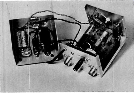
Fig. 167 - The vfo calibrator assembly. Power supply components are mounted
on the bottom cover of the aluminum enclosure.
The 100-kHz crystal oscillator, the two-stage wave-shaping amplifier, the diode product detector, and the three stage audio amplifier are all assembled on a 3- by 4-1/2- inch phenolic circuit board. This method of construction results in a rugged, compact instrument. The drilling template for the vfo calibrator is shown in the back of this Manual; a component placement dia gram and a photograph of a completed assembly are shown in Figs. 166 and 167, respectively.
CIRCUIT NO. 29- MOTOR-SPEED CONTROL
The motor-speed-control circuit provides both speed control and speed regulation (constant speed under conditions of changing load) for ac/dc universal motors (motors that are series wound). The circuit also provides smooth anti-skip operation at reduced speeds and is useful for adjusting and regulating the speed of power tools, such as drills, buffers, and jig saws; hair dryers; floor polishers; and commercial food mixers. When the circuit is used with a power drill, the speed of the motor can be made slow enough so that the drill can be used as a screwdriver.
The motor-speed-control circuit is suitable for use with motors that have nameplate ratings up to 6 amperes.
Motor speed can be adjusted from complete cutoff to essentially full rated value.
------------
Parts List
C1 C2 = 0.01 microfarad, 1000 volts, ceramic
Cg = 250 microfarads, 6 volts, electrolytic
C4 = 1 microfarad, 200 volts, ceramic
CR, CR2* = silicon rectifier, RCA SK3016 mounted in a fuse clip for heat sinking
CR8 through CR10* - silicon rectifier, RCA SK3030
F1 = fuse, 125 volts, 1 ampere, rating depends on intended load
Q1 = transistor, RCA SK3005
Q2 = transistor, RCA SK3020
R1 = potentiometer, 100,000 ohms, 2 watts, linear taper
R3 = 150 ohms, 1/2 watt, 10% 118 Re = 470 ohms, 1/2 watt, 10% R4 = adjustable resistor, 1 ohm, 25 watts, Ohmite No. 0360 or equivalent
Rs R7 = 1000 ohms, 1/2 watt, 10% Rs = 15,000 ohms, 1 watt, 10% R912 11 = 5600 ohms, 1/2 watt, 10% 12 10 = 100 ohms, 1/2 watt, 10% SI = switch, 125 volts, 6 amperes, single-pole, single-throw SCR, SCR,* = silicon controlled rectifier RCA KD2100
*These components are available in two KD2105 RCA Silicon Controlled Rectifier Experimenter's Kits.
Fig. 168 - Schematic diagram and parts list for the motor-speed control.
-------------------
Circuit Operation
The schematic diagram and parts list for the motor-speed control are shown in Fig. 168. Motor speed is determined by the time that one of the SCR's conducts during each half-cycle of ac input. This time is controlled by adjustment of the potentiometer.
When the potentiometer is set for minimum resistance (control knob in maximum clockwise position), capacitor C4 charges very rapidly and the triggering-voltage level of the two transistor regenerative switch is reached early in each half-cycle. When the transistors in the regenerative switch start conducting, capacitor C4 discharges rapidly through the series circuit made up of the transistors and resistor R10. The capacitor discharge causes a pulse across the parallel circuit composed of R1, and the gate circuits of the SCR's. If the anode of SCR, is positive with respect to the cathode, the anodes of diodes CR5 and CR9 are also positive with respect to their cathodes and the diodes conduct.
A conduction path then exists between the junction of C4 and RIP and the cathode of SCR 1 through CR5. The pulse appearing across the parallel combination of R10 and the SCR' gate circuit (CR3 , the gate, and C4) causes SCR 1 to conduct. At the same time, SCR2 is non-conducting because its anode is negative with respect to its cathode; C R6 and CR8 are non-con ducting for the same reason. Reverse polarity on SCR 2, CR6, and CR8 applies a reverse polarity to CR4 and prevents the pulse from R10 from reaching the SCR2 gate.
During the next half-cycle, the polarity of the power source reverses, and SCR 2 becomes the conducting SCR; SCR 1 becomes the non-con ducting SCR.
As the resistance of the potentiometer is increased, the time required to charge C4 to the triggering potential of the regenerative switch becomes longer, and the pulse is produced later in the half-cycle, or not at all if the charge on C4 does not reach triggering level. Therefore, the speed of the universal motor can be controlled by the position of the potentiometer knob.
When the mechanical load on the motor is increased, :he motor demands more current. The increase in current causes an increase in voltage across the 1-ohm adjustable sensing resistor R4 . This voltage is fed back through diode CR7 and resistor R9 to the base of Q2 , one of the components of the regenerative switch. The application of this voltage to the base of Q2 reduces the triggering voltage required by the regenerative switch and causes it to conduct earlier in the half-cycle. Thus, more power is delivered to the motor so that it can maintain a constant speed. Diodes CR 1 and CR 2 prevent current from flowing through R4 to the feedback network during the half-cycle in which SCR 2 is not conducting.
Resistor R4 is set according to motor nameplate rating or load current; the proper setting for this resistor can be determined from the curve shown in Fig. 169.
Diode CR 10 is used to prevent improper timing of the triggering circuit when the potentiometer is set high enough so that C4 does not reach triggering voltage. If the charge on C1 has not reached triggering potential at the end of a half-cycle, this diode triggers the regenerative switch into conduction so that any residual charge on C4 is dissipated. The anti-skip circuit composed of CR io and R7 ensures that each half-cycle of operation starts under the same conditions and thus provides smooth, continuous motor operation.
--------------
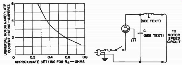
Fig. 169 - Approximate setting of R 4 for various motor nameplate ratings.
Fig. 170 - Schematic diagram of L-filter connections.
---------------
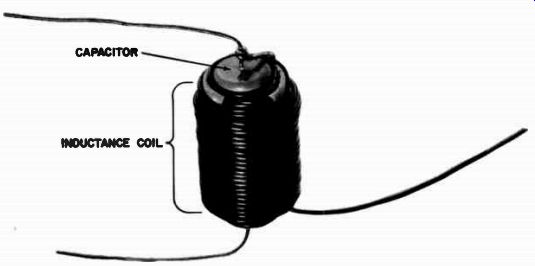
Fig. 171 - Photograph of the L-filter to reduce radio-frequency interference.
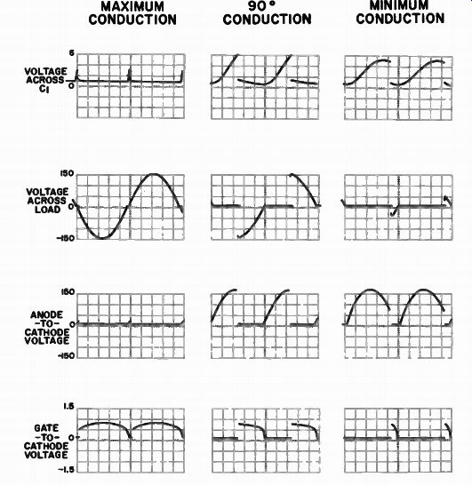
Fig. 172 - Typical waveshapes taken at various points in the motor -speed-control
circuit.
---------------
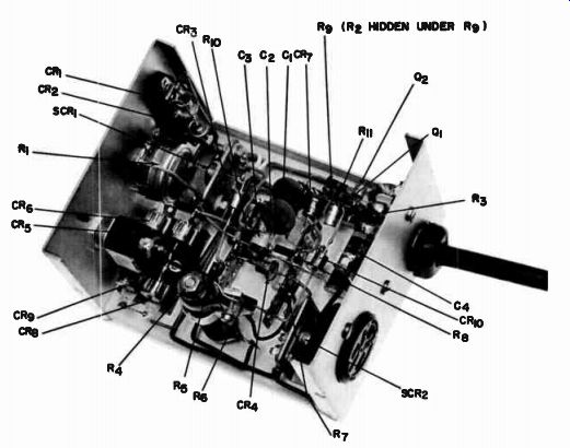
Fig. 173 - A suggested method of constructing the motor-speed control in a
3- by 4- by 5-inch aluminum box.
Adjustments and Special Considerations
This circuit may produce some radio-frequency interference; such interference can be minimized by the installation of an L-filter between the circuit and the voltage source and load as shown in Fig. 170. The filter consists of about 18 feet of No. 18E wire "scramble" or random-wound on a 0.5-inch-diameter rod, and a 0.05 microfarad 200-volt paper capacitor.
If desired, the capacitor can be used as the core of the coil instead of the rod.
If this method is used, a 600-volt capacitor should be used instead of a 200-volt type. The larger 600-volt capacitor is used only because it provides a better physical core size.
Fig. 171 is a photograph of the L-filter.
Operation of single-speed motors at reduced speeds should be limited to relatively short periods. Most motors intended for single-speed operation depend on the air flow provided by a built-in fan to keep the temperature rise within acceptable limits. When the motor speed is reduced, this air flow also decreases, and the motor may become overheated.
The waveshapes shown in Fig. 172 are typical of those present at various points in the motor-speed-control circuit.
Construction
A suggested method of constructing the motor-speed-control in a 3- by 4 by 5-inch aluminum box is shown in Fig. 173.
CIRCUIT NO. 30- MODEL TRAIN AND RACE CAR SPEED CONTROL
The model train and race-car speed control provides continuous and smooth control (from stop to full speed) of most model railroad trains, race cars, and similar "hobby"-type vehicles designed to operate at dc voltage up to 12 volts.
Circuit Operation
The schematic diagram and parts list for the model train and race-car speed control are shown in Fig. 174.
The operating speed of the model rail road train or race car with which this circuit is used is determined by the delay involved in triggering the SCR into conduction after the start of each half-cycle of ac input voltage. This delay time, in turn, is controlled by adjustment of the potentiometer R1. Because the load and the SCR are in parallel, output voltage is available at the load only when the SCR is not conducting. When the control knob is set to its maximum clockwise position, therefore, maximum delay in triggering the SCR is obtained and maximum speed is attained in the model vehicle.
When switch S1 is closed, the pulsating direct current from the bridge rectifiers charges capacitor C2 through resistor R2 and diode CR5, and a voltage appears across the output terminals. Under conditions of minimum conduction of the SCR (approximately 55 percent of each input half-cycle of voltage), a maximum voltage of approximately 13 volts is present at the output terminals. As the control knob is turned in a counterclockwise direction, the resistance of R1 is decreased and the current through R1, R3 , and R8 charges capacitor C1 more quickly to the triggering potential of the two transistor regenerative switch. The switch, in turn, triggers the SCR into conduction, and the voltage across the 3utput terminals drops to slightly less than one volt when the control knob is n the most counterclockwise position.
Because capacitor C2 performs an integrating function, the output voltage approaches a steady dc level deter mined by the relative duration of the "ON" and "OFF" periods of the SCR. The silicon rectifier CR5 isolates the anode of the SCR from the potential on C2 so that the capacitor cannot discharge through the SCR when it is triggered into conduction and so that the anode voltage falls to zero and turns off the SCR at the end of each input half-cycle. Resistor R7 helps to stabilize the operation of the SCR, and also provides a parallel path for discharge of C1 after the SCR is triggered into conduction. Resistor R2 limits the current through the bridge rectifier circuit to the maximum allowable value of two amperes in the event of a short circuit across the output terminals.
The parallel arrangement of the load and the SCR in this circuit provides superior control and speed regulation at the operating voltages of model vehicles. The circuit is inherently self-regulating, i.e., it maintains essentially constant speed under varying load conditions. When the mechanical load increases, (e.g., when the vehicle travels on an inclined portion of the track or road), the vehicle motor tends to slow down. The motor current then increases, and the voltage across capacitor C2 decreases. However, because this voltage is also the potential for the timing circuit (R1 , R3, R8, and C1 ), the capacitor C1 charges more slowly and the delay in triggering the SCR is increased. As a result, the output voltage is also increased and the speed is maintained essentially constant.
---------------------
Parts List
CI = 1 microfarad, 200 volts, paper Cy = 1000 microfarads, 25 volts, electrolytic CR 1 CR 2 CR3 CR4 CR6* silicon rectifier, RCA SK3016, mounted in fuse clips for heat sinking F1 = fuse, 125 volts 1 ampere, I = lamp, neon, NE-2 or equivalent Q1 = transistor , RCA SK3005 Q2 = transistor, RCA SK3020 R = potentiometer, 1000 ohms, 2 watts, linear taper Ry = 15 ohms, 60 watts (three 5-ohm 20-watt resistors connected in series)
R, R7 = 100 ohms, 1/2 watt, 10% R4 = 150 ohms, 1/2 watt, 10% R5 = 470 ohms, 1/2 watt, 10% R6 = 1000 ohms, 1/2 watt, 10% 128 = 15 ohms, 1/2 watt, 10% R9 = 47,000 ohms, 1/2 watt, 10% SI = switch, 125 volts, 1 ampere, single-pole, single-throw SCRI* = silicon controlled rectifier, RCA KD2I00
T1 = power transformer, Stancor No.
RT-202 or equivalent
*These components are available in a single KD2 105 RCA Silicon Con trolled Rectifier Experimenter's Kit.
------------------
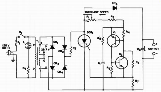
Fig. 174 - Schematic diagram and parts list for model train and race-car speed
control.
Fig. 175 shows the waveshapes across the SCR (from anode to cathode) for one cycle of input voltage at (a) full speed, (b) half speed, and (c) zero speed. At the start of each half cycle (point I), the SCR is off. The anode voltage then follows the increasing sine wave until it equals the voltage on capacitor C (point 2). The diode CR, then starts to conduct, and Ca charges until the SCR is triggered into conduction (point 3) by the timing portion of the circuit. At the start of conduction, the anode drops to 0.6 volt (point 4), the diode CR, stops conducting, and capacitor C2 discharges into the load until point 2 of the next half cycle.
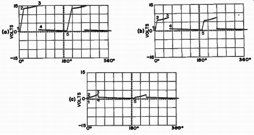
Fig. 175 - Typical waveshapes across the SCR in the model train and race-car
speed control at (a) full speed, ( b) half speed, and (c) zero speed.
Construction
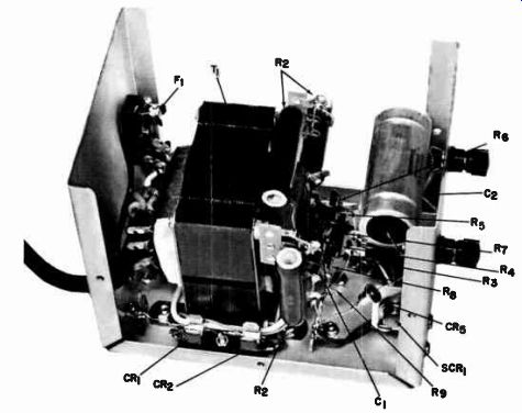
Fig. 176 - The model train and race-car speed control assembled in a 3 - by
4 - by 5 - inch aluminum box. Components not identified are hidden.
The SCR stops conducting when the input voltage drops to zero at the end of the half-cycle (point 5). The load-voltage waveshape is described by Fig. 176 shows a model train and the charge and discharge paths of race-car speed control assembled in a capacitor C. 3- by 4- by 5-inch aluminum box.
CIRCUIT NO. 31-ELECTRONIC FLASHER
The electronic flasher circuit sup plies power in short on-off pulses to ac/dc devices that have total power ratings up to 240 watts (nameplate current ratings up to two amperes) and that do not use the frame of the device as a ground. The time of each "ON" pulse is fixed at approximately one half second. The time of each "OFF" pulse can be adjusted to provide the desired number of "ON" pulses per minute.
This circuit is useful for controlling the flashing of incandescent-lamp loads (e.g., in Christmas-tree decorations, advertising signs, warning signals, and flashing tower lights) and for actuating an auditory device (e.g., an alarm bell).
----------------
Parts List
C1 = 50 microfarads, 15 volts, electrolytic Cs = 50 microfarads, 150 volts, electrolytic CR1 CR2 CR3 CR4* = silicon rectifier, RCA SK3016 mounted in fuse clips for heat sinking F1 = fuse, 125 volts, 3 amperes
= lamp, neon, NE-83 or equivalent Q1 = transistor, RCA SK3005 Q2 = transistor, RCA SK3020 R1 = potentiometer, 10,000 ohms, 2 watts, linear taper R2 = 3000 ohms, 5 watts, 10% R3124 = 2200 ohms, 1/2 watt, 10% R5 = 680 ohms, 1/2 watt, 10% R8 = 47,000 ohms, 1/2 watt, 10% R7 = 4700 ohms, 1/2 watt, 10% R8 = 22,000 ohms, 1/2 watt, 10% R8 = 150 ohms, 1/2 watt, 10% SI = switch, 125 volts, 3 amperes, single-pole, single-throw SCRI* = silicon controlled rectifier, RCA KD2I00
*These components are available in a single KD2105 RCA Silicon Con trolled Rectifier Experimenter's Kit.
--------
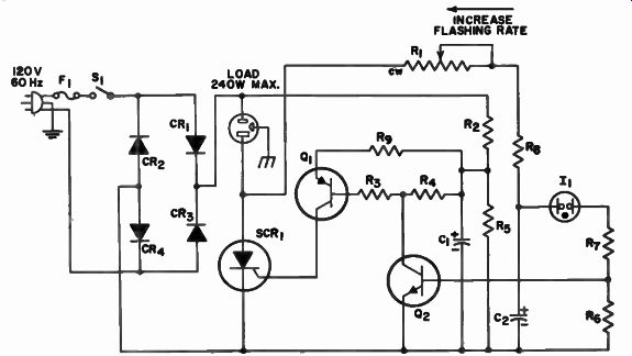
Fig. 177 - Schematic diagram and parts list for the electronic flasher.
-----------
Circuit Operation
The schematic diagram and parts list for the electronic flasher are shown in Fig. 177. The power pulse rate (or the length of time between "ON" periods) is determined by the time required to charge the timing capacitor C2to the value required to turn on the neon lamp. The charging time for capacitor C2 is controlled by adjustment of potentiometer R
Fig. 178 - The electronic flasher assembled in a 3- by 4- by 5-inch aluminum
box.
When switch S1 is closed, the pulsating dc voltage from the bridge rectifier circuit is applied across the load and the parallel combination of the SCR and the resistance-capacitance circuit R1 , R8, and Cz. Because the SCR is not conducting, load current is negligible. Therefore, the input pulses charge C2, through resistor R1 and R8, to the firing potential (approximately 80 volts) of the neon lamp. When the neon lamp fires, the current through resistor R7 (approximately two milliamperes) serves as the input signal to the base of transistor Q2 . Transistors Q7 and Q2 are used in this circuit as a two-stage amplifier.
Resistor ft 6 in the base-emitter circuit of Q2 ensures that the transistors remain cut off when Ii is not conducting. The output for the two-stage amplifier triggers the SCR into conduction, and the full pulsating dc input appears across the load (the SCR is a short circuit across R1, R8, and C2). Load current continues to flow for practically 180 degrees of each succeeding half-cycle of input signal until C2 discharges to the extinction voltage of the lamp. (The SCR is actually cut off near the end of each half-cycle and retriggered shortly after the beginning of each succeeding half-cycle by the current applied to the transistors as a result of the storage energy in capacitor C1 .) When the charge on C2 is insufficient to maintain conduction in the neon lamp, there is no input to the two-stage transistor amplifier, the flow of gate current to the SCR ceases, and the SCR is not triggered into conduction on the next half-cycle of input.
The load current then drops to a negligible value, and the operating cycle starts again.
Adjustments and Special Considerations
The rate of discharge for C2, and therefore the "O'4" time for the flasher, is controlled by the value of resistor 112; the value shown in Fig. 177 provides an "ON" pulse of approximately one-half second. The charging rate for C2 and therefore the "OFF" time for the flasher, is controlled by means of potentiometer R1 . For warning-signal applications, R1 is normally adjusted to provide 40 flashes per minute, with an "ON" time of one-half second and an "OFF" time of one second. Resistors R2 and R5 and capacitor C1 constitute the power sup ply for the two-stage transistor amplifier; Rs is a current-limiting resistor for transistor Q1.
Fig. 178 shows the electronic flasher assembled in a 3- by 4- by 5 inch aluminum
box.
CIRCUIT NO. 32- ELECTRONIC TIME DELAY
The electronic time delay circuit is useful for actuating an auditory dev ice to signal the end of a time interval (e.g., to limit card or chess players to one minute of "thinking time"), or for making another device "wait" for a short time until some action can be accomplished (e.g., getting into the picture before the camera clicks). The circuit is used to delay the application of power to a load for a predetermined period after the control switch is turned on and can be used with ac/dc devices that do not use the frame of the device as a ground and that have total power ratings up to 240 watts (nameplate current ratings up to two amperes). The delay time can be adjusted from five seconds to approximately two minutes.
Circuit Operation
The schematic diagram and parts list for the electronic time delay are shown in Fig. 179. The delay in turn-on time of the equipment with which this circuit is used is determined by the length of time required for the timing capacitor C 2 to charge to the value required to turn on the neon lamp NE 83 and trigger the two-transistor switch. This time, in turn, is controlled by adjustment of the resistance of potentiometer
When switch S1 is ON, the full wave rectified current from the rectifier bridge circuit charges capacitor C1 through resistor R2. The charge on C1 is held to a peak potential of less than seven volts by the voltage divider formed by resistors R2 and R2 . At the same time, the timing capacitor C2 starts to charge through series resistors R1 and R3. When the charge on C2 reaches a value of about 80 volts, the neon lamp fires and triggers the two transistor regenerative switch. The conducting regenerative switch completes the gate circuit through resistor Re and triggers the SCR into conduction. The fixed charge on C1 then maintains conduction in the regenerative switch through the gate of the SCR, and load current continues to flow for the duration (practically 180 degrees) of each succeeding half-cycle of input voltage until S1 is turned OFF. (The SCR is actually cut off near the end of each half-cycle and retriggered shortly after the beginning of each
succeeding half-cycle by the current applied as a result of the steady potential on C1 .) In the OFF position, S1 discharges C2 through resistor R9 and prepares the circuit for the next time delay application.
----------
Parts List
C1 = 50 microfarads, 15 volts, electrolytic C: = 50 microfarads, 150 volts, electrolytic CRICR:CR:CR4* = diode, RCA SK 3016 mounted in fuse clip for heat sinking F: = fuse, 125 volts, 3 amperes Ii = lamp, neon, NE-83 or equivalent Q1 = transistor, RCA SK3004 Q2 = transistor, RCA SK3020 R1 = potentiometer, 1 megohm, 2 watts, linear taper R9 = 3000 ohms, 5 watts, 10% R3 = 47,000 ohms, 1/2 watt, 10% 114 = 10,000 ohms, 1/2 watt, 10% R6 = 150 ohms, 1/2 watt, 10% R6 = 470 ohms, 1/2 watt, 10% R7 = 180 ohms, 1/2 watt, 10% 118 = 100 ohms, 1/2 watt, 10% R9 = 33 ohms, 1/2 watt, 10% Si = switch, 125 volts, 3 amperes, double-pole, double-throw, toggle SCR,* = silicon controlled rectifier, RCA KD2100
*These components are available in SCR Silicon Controlled Rectifier Experimenter's Kit KD2105.
-------------
Fig. 179 - Schematic diagram and parts list for the electronic time delay.
-----------------
Adjustments and Special Considerations
With the values shown in the parts list for R1, R3, and C2 , this circuit can be set for time delays from five seconds to approximately two minutes by adjustment of potentiometer R1 . Although longer time delays can be obtained by the use of a larger value for the timing capacitor C2, it is not economically feasible to obtain delays of much more than five minutes with this circuit.
The exact length of the time delay will depend on the actual capacitance of C2. Most electrolytic capacitors are rated on the basis of minimum guaranteed value (MGV), and the capacitor used may have a value much higher than its rating. The circuit should be calibrated for various positions of the control knob after the timing capacitor has had a chance to age. Once the capacitor has reached its stable value, the precision of this timer should be well within the requirements of most applications.
Fig. 180 shows the electronic time delay assembled in a 3- by 4- by 5-inch aluminum box.
Fig. 180 - The electronic time delay assembled in a 3- by 4-by 5-inch aluminum box.
CIRCUIT NO. :33 - AUDIO-FREQUENCY-OPERATED SWITCH
The audio-frequency-operated switch circuit can be used to turn on a load rated up to one kilowatt when the sound level increases above a predetermined level. The load continues to receive power until the sound level drops below the predetermined level.
The circuit can be activated by an audio signal provided by a preamplifier such as that described in Circuit No. 7; the preamplifier is driven by a microphone. The circuit can be used to control electrical systems, such as alarms, transmitters, and remote intercoms. It can also be used to measure noise level; in such applications, it activates some device when a predetermined noise level is reached. The level of input to this switch should be approximately 1 volt. The RCA Experimenter's Kit, KD-2112, contains all parts needed to make an integrated-circuit amplifier that will satisfy the input preamplifier requirements of the audio-frequency operated switch.
------------
Parts List
C1 C2 = 10 microfarads, 15 volts, electrolytic C3 ... 0.1 microfarad, 25 volts or greater C4 = 10 to 100 microfarads, 12 volts, electrolytic, to increase release time CR1 CR2 CR2CR4 = silicon rectifier, RCA SK3030 CR6 C1 to* = silicon rectifier, type 1N34A F1 = fuse, 125 volts, ampere rating depends on load
- transistor, RCA SK3005 R1 - potentiometer, 5000 ohms, 2 watts, linear taper R2 R4 = 4700 ohms, 2 watts, 10% 11 3 = 270 ohms, 1/2 watt, 10% R5 = 470 ohms, 1/2 watt, 10% Si = switch, 125 volts, 15 amperes, single-pole, single-throw toggle SCR, SCR2* = silicon controlled rectifier, RCA KD2100
*These components are available in two RCA Silicon Controlled Rectifier Experimenter's Kits KD2105.
------------ Fig. 181 - Schematic diagram and parts list for the audio-frequency-operated switch.
---------------
Circuit Operation
The schematic diagram and parts list for the audio-frequency-operated switch are shown in Fig. 181. The audio- or radio-frequency signal applied to the input terminals in rectified by CR5 and CR6. The resulting signal is applied to the base of Q1 through the potentiometer R1. The amount of noise required to activate the circuit can be controlled by adjustment of the potentiometer. The signal applied to the base of Q1 causes it to conduct provided that the emitter of Q 1 is positive. The current conducted by Q1 charges C2 through the charging path 013, CR, and R4 . On the following half-cycle, the charge on capacitor C 2 is applied to the gate of SCR2 and turns it on; a voltage is thus placed across the load.
The load voltage is also applied to the combination of CR1, R2 and C1, and causes the capacitor to charge. The charge on C1 turns on SCR, during the next half-cycle. This process repeats as long as there is a sufficient audio- or radio-frequency signal present at the input terminals to cause Q to conduct.
When the signal is removed, Q becomes nonconductive; the charging path for capacitor C2 is thus opened. If C2 cannot charge, SCR, cannot turn on. The result is an open circuit to the load. Because there is no voltage across the load, capacitor C1 cannot obtain the charge it needs to turn on SCR, during the next half-cycle. Therefore, both SCR's remain off until another signal is received at the input terminals.
The release time. or the time that it takes for the switch to turn off after the input signal ceases, can be increased so that the switch does not open during momentary interruptions (e.g., between syllables). This increase in release time is accomplished by connection of a capacitor between the emitter and the collector of (b. Values of capacitance up to 100 microfarads (15 volts) can be used.
Construction
Fig. 182 - The audio-frequency-operated switch assembled in a 3- by 4- by 5-inch aluminum box.
The photograph in Fig. 182 shows the audio-frequency-operated switch assembled in a 3- by 4- by 5-inch aluminum box.
CIRCUIT NO. 34-FREQUENCY-SELECTIVE AF AMPLIFIER
The frequency-selective af amplifier amplifies signals at only one predetermined frequency. At that frequency the voltage gain is 20 to 30; at other frequencies the voltage gain is unity or less. Circuits of this type are useful in screening out undesirable side signals when copying code or for identifying the frequency of a particular signal.
--- Parts List C1 C3 C4 = 0.1 microfarad, 25 volts or greater 10 microfarads, 6 volts, electrolytic
= 680 picofarads, 25 volts or great or 1500 picofarads, 25 volts or greater MOS field-effect transistor, type 3N141 C2 = C5C6 C7 = Q1 = R1 = I megohm, 1/2 watt, 10% R2 = 100,000 ohms, 1/2 watt, 10% Ra = 6800 ohms, 1/2 watt, 10% R4 = 1200 ohms, 1/2 watt, 10% R5 R6 = 220,000 ohms, 1/2 watt, 10% R7 = potentiometer, 250,000 ohms, linear taper R8 = potentiometer, 1 megohm, linear taper
Circuit Operation
The schematic diagram and parts list for the frequency-selective af amplifier circuit are shown in Fig. 183.
Potentiometer R8 controls the level of the feedback signal; potentiometer R7 is used to adjust or peak the twin-T bridge to the desired frequency. Transistor Q1 acts as a basic audio amplifier. Part of the output of the amplifier is applied to the twin-T bridge oscillator through C3 . At the predetermined frequency, where most gain occurs, the filter passes the ac at a phase angle that assures positive feedback. The feed back, adjusted by R8, is added to the incoming signal and causes it to increase.
With the component values shown in the parts list, the frequency of the bridge oscillator and the frequency selected for amplification is approximately 1000 Hz; Table VIII shows values of C5 , C6 , and C7 required for other typical frequencies.
The current drain for this circuit is approximately 1.5 milliamperes. The maximum input signal is 0.1 volt rms.
Fig. 183 - Schematic diagram and parts list for the frequency-selective al amplifier.
Table VIII. Frequency-Selective AF Amplifier Bridge Capacitor Values for Various Frequencies
Fig. 184 - Component placement diagram for the frequency-selective amplifier.
Construction
The only special care required in the building of this circuit is in the handling of the MOS transistor. The procedure outlined in the section on Mechanical Considerations must be followed. The drilling template for the frequency-selective af amplifier is shown at the back of the Manual; a component placement diagram and a photograph of a completed circuit board are shown in Figs. 184 and 185, respectively.
Fig. 185 - Completed circuit board for the frequency-selective amplifier.
CIRCUIT NO. 35--AUTOMOBILE LIGHT MINDER
This circuit sounds an alarm if the lights of a car are left on when the ignition is turned off. The alarm stops when the lights are turned off. When the lights are intentionally left on for a period of time, the alarm can be defeated so that no warning sounds.
The alarm then sounds when the ignition switch is turned on as a reminder that the system has been defeated and that the switch should be returned to its normal position.
Circuit Operation
Schematic diagrams for a positive ground and a negative-ground light minder are shown in Fig. 186. The circuit is essentially an oscillator that obtains its supply voltage from two possible sources, the ignition system or the light system of the car. In the normal mode of operation, the ignition system is connected to the collector circuit of Q1 and the light system is connected through CR1 to the emitter of Ql. When the ignition switch is on, the collector of the transistor is at the supply voltage. If the lights are on at the same time, the transistor emitter is also at the supply voltage.
Because both the emitter and the collector are at the same voltage, the circuit does not oscillate and no alarm sounds. When the ignition is turned off, the collector is returned to ground through R1 and C1 , but the emitter remains at the supply voltage and provides the necessary bias for the circuit to oscillate. Turning the lights off removes the supply voltage and stops the oscillation.
In the defeat mode of operation, the ignition system is connected through CR 1 to the transistor emitter; the light system is completely disconnected. The lights can then be turned on without the alarm sounding. When the ignition is turned on, it supplies the necessary voltage to the transistor emitter to cause the alarm to sound.
When the alarm is sounding the light-minder current drain is 23 milliamperes; when the alarm is not sounding the current drain is 3 milliamperes.
-------------------
Parts List
C1 = 30 microfarads, 25 volts, electrolytic
Cs = 0.22 microfarad, 25 volts or greater
CR1 = silicon rectifier, RCA SK3030
R1 = 15,000 ohms, 1 watt, 10%
Rs = 680 ohms, 1/2 watt, 10%
Q1 = transistor, for negative-ground system, RCA SK3005; for positive-ground system, RCA SK3020
S1 = switch, double-pole, double throw
Speaker = 3.2 ohms
T1 = Output transformer, primary 500 ohms center tapped, secondary 3.2 ohms, Stancor No.
TA-42 or equivalent
------ Fig. 186 - Schematic diagram and parts list for the automobile light
minder: (a) negative ground system, ( b) positive ground system.
------
++++++++++++