Introduction
ONE of the most outstanding developments in electronics since the Second World War has been the introduction of the transistor, a minute semiconducting device which can perform most functions of a thermionic valve but with far greater efficiency. A transistor may be smaller than a ¼ in. cube, has no heater, may consume less than 1 mA from a 3-volt source, yet can be as effective as an amplifier or oscillator as a thermionic valve consuming, say, 50 mA of filament current at 1.4 volts and 2 mA of anode current at 60 volts. In addition to its greater efficiency, the transistor is non-microphonic and has a life many times that of a valve. Early junction transistors operated satisfactorily up to a few Mhz only, but modern (drift) types can be used above 100 Mhz. The output power of transistors has also steadily increased and a modern power transistor can deliver several watts in class-A operation.
One disadvantage of transistors compared with thermionic valves is that the current they draw from the h.t. supply increases with temperature. The dissipation produced by this current in the transistor itself generates heat and a regenerative action is possible, ending in a rapid rise of current which can damage or even destroy the transistor. This phenomenon is termed thermal runaway and, where danger of it exists, the circuits associated with the transistor must be designed to prevent runaway by making the current drawn from the supply less dependent of ambient and of transistor temperature. Stabilization circuits of this type are discussed fully in Chapter 6. The danger of thermal runaway is a very real one in germanium transistors, and most of the transistors in use at present employ this element. For silicon transistors the usable range of temperature is much greater--and the danger of thermal runaway at normal operating temperatures is much less.
Although a transistor can perform nearly all the functions of a valve, such as detection, amplification, oscillation, pulse-generation and frequency changing, its properties are different from those of a valve and it therefore requires specialized circuitry. The principal difference is in the input and output resistances and in the internal feedback of the transistor. For a transistor the input is small compared with the output resistance, and to obtain efficient operation the associated circuit must be designed to allow for this.
The internal feedback must in many circuits be neutralized or otherwise allowed for.
Possibly the most obvious application for transistors is in deaf-aid equipment where their small size makes possible the construction of unobtrusive amplifiers which can, in fact, be built into the framework of spectacles. Such amplifiers can operate for long periods on a single 1.5-volt cell and have very low running costs.
Transistors have already supplanted valves in portable radio receivers and here too they have made possible a substantial reduction in running costs. A receiver may need five or six transistors to give a performance comparable with that of a four-valve battery driven superhet but the average current consumption is not likely to exceed 25 mA at 6 volts, which represents less power than is consumed by the filaments alone of the valve receiver. Transistors are well suited for use in car radio receivers because they operate well on a 6-volt or 12-volt supply such as a car battery. Thus a completely-transistorized car radio requires only a 6-volt or 12-volt supply and there is no need for the bulky and noisy vibrator or rotary unit required in an all-valve car radio to supply the h. t. Thermionic valves can give a useful performance as voltage amplifiers and frequency changers even when operated from an h.t. supply as low as 12 volts but they cannot deliver the power output expected from a car radio from such a low-voltage supply.
A transistor can, however, deliver the required a.f. output from such a supply and it is therefore possible to construct a 12-volt car radio with valves in all stages except the last which is transistorized.
Such a radio is termed a hybrid type and it has the advantage of the fully-transistorized type that it eliminates the need for an h.t. unit.
Some care is needed in the design of a car radio including transistors to protect them from thermal runaway because it is possible to obtain high temperatures inside a closed car on a hot summer day.
Transistors are well suited for use in portable public-address amplifiers, and it is possible to construct equipment to deliver, say, 20 watts of power, which operates from a 6-volt or 12-volt supply.
Transistors have been used in telephone equipment such as repeaters and also in walkie-talkie equipment. Transistor transmitters and receivers have even been successfully operated from solar cells (i.e. cells which derive their power from the sun): the running cost of such equipment is literally nothing.
DEFINITION OF A SEMICONDUCTOR
The heart of a transistor consists of semiconducting material, e.g., germanium or silicon and the behavior of the transistor largely depends on the properties of this material. As the name suggests a semiconducting material is one with a conductivity lying between that of an insulator and that of a conductor: that is to say one for which the resistivity lies between, say, 10^12 ohm-cm (a value typical of glass) and 10^-6 ohm-cm (approximately the value for copper). Typical values for the resistivity of a semiconducting material lie between 1 and 100 ohm-cm.
Such a value of resistivity could, of course, be obtained by mixing a conductor and an insulator in suitable proportions but the resulting material would not be a semiconductor. Another essential feature of a semiconducting material is that its electrical
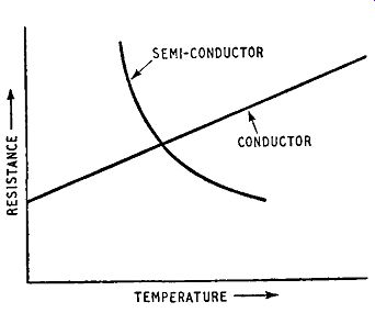
Fig. 1.1. Resistance-temperature, relationship for a conductor and a semiconductor
resistance decreases with increase in temperature over a particular temperature range which is characteristic of the semiconductor.
This behavior contrasts with that of elemental metallic conductors for which the resistance increases with rise in temperature. This is illustrated in Fig. 1.1, which gives curves for a conductor and a semiconductor. The curve for the conductor shows the resistance increasing linearly with increase in temperature, whereas that for the semiconductor shows the resistance decreasing exponentially with increase in temperature. Over the significant temperature range the relationship between resistance and temperature for a semiconductor could be written: Rt= aeb/T
... where Rt is the resistance at an absolute temperature T, a and b being constants characteristic of the semiconducting material. The two curves in Fig. 1.1 are not to the same vertical scale of resistance.
All semiconducting materials exhibit the temperature dependence discussed in the paragraphs above in the pure state: the addition of impurities raises the temperature at which the material exhibits this behavior, i.e. the region of negative temperature coefficient.
Germanium in its pure state is a poor conductor, the resistivity being 46 ohm-cm at 27° C, and is of little direct use in transistor manufacture. However, by the addition of a very small but definite amount of a particular type of impurity, the resistivity can be reduced and the material made suitable for transistors.
Germanium and silicon so treated are extensively employed in the manufacture of transistors.
The behavior of semiconductors can be explained in terms of atomic theory. The atom is assumed to have a central nucleus which carries most of the mass of the atom and has a positive charge.
A number of electrons carrying a negative charge revolve around the nucleus. The total number of electrons revolving around a particular nucleus is sufficient to offset the positive nuclear charge, leaving the atom electrically neutral. The number of electrons associated with a given nucleus is equal to the atomic number of the element. The electrons revolve in a number of orbits and, for the purpose of this discussion, the orbits may be regarded as concentric, the nucleus being at the centre, as shown in Fig. 1.2. This diagram is greatly simplified; the orbits are in practice neither concentric nor co-planar.
The first orbit (sometimes called a ring or a shell) is complete when it contains 2 electrons, and an atom with a single complete shell is that of the inert gas, helium. The second ring is complete when it has 8 electrons, and the atom with the first 2 rings complete is that of the inert gas, neon. The third ring is stable when it has 8 or 18 electrons, and the atom having 2, 8 and 8 electrons in the 1st, 2nd and 3rd rings is that of the inert gas, argon.
All the inert gases have their outermost shells stable. It is difficult to remove any electrons from a stable ring or to insert others into it. Atoms combine by virtue of the electrons in the outermost rings: for example, an atom with one electron in the outermost ring will willingly combine with another whose outermost ring requires one electron for completion.
The inert gases, having their outer shells stable, cannot combine with other atoms or with each other. The number of electrons in the outermost ring or the number of electrons required to make the outermost ring complete has a bearing on the chemical valency of the element and the outermost ring is often called the valence ring.
Now consider the copper atom: it has 4 rings of electrons, the first 3 being complete and the 4th containing 1 electron, compared with the 32 needed for completion. Similarly the silver atom has...
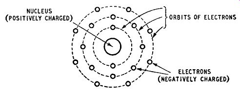
Fig. 1.2 Simplified diagram of structure of atom: for simplicity, electron
orbits are shown as circular and co-planar
... 5 rings, 4 stable and the 5th also containing 1 out of 50 needed for completion. The atoms of both elements thus contain a single electron and this is loosely bound to the nucleus. It can be removed with little effort and is termed a free electron. A small e.m.f. applied to a collection of these atoms can set up a stream of free electrons, i.e., an electric current through the metal. Elements in which such free electrons arc available are good electrical conductors.
It might be thought that an atom with 17 electrons in the outer most orbit would be an even better conductor, but this is not so.
If one electron is added to such an orbit it becomes complete and a great effort is needed to remove it again.
The arrangement of orbital electrons in a germanium atom is pictured in Fig. 1.3. There arc 4 rings, the first containing 2 electrons, the second 8, the third 18, and the 4th (final) 4. The total number of electrons is 32, the atomic number of germanium. The corresponding diagram for the silicon atom is given in Fig. 1.4, the three rings containing 2, 8 and 4 electrons respectively. The total number of electrons per atom is 14, the atomic number for silicon. A significant feature of these two atomic structures is that
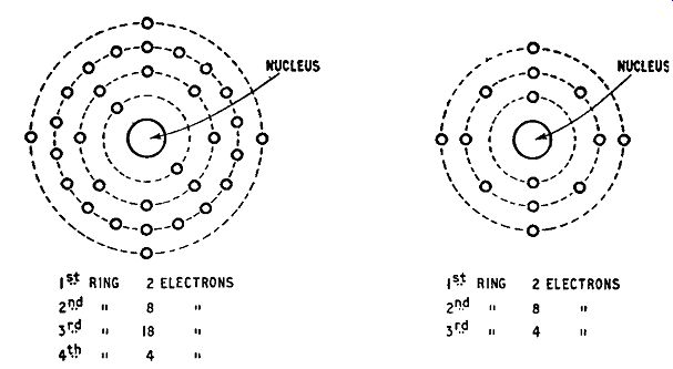
Fig. 1.3. Structure of germanium atom; Fig. 1.4. Structure of silicon atom
the outermost ring contains 4 electrons: both elements belong to Group IV
of the Periodic Table.
COVALENT BONDS
It might be thought that some of the 4 electrons in the valence ring of the germanium or silicon atom could easily be displaced and that these elements would therefore be good conductors. In fact, crystals of pure germanium and pure silicon are very poor conductors. To understand this we must consider the relationships between the valence electrons of neighboring atoms when these are arranged in a regular geometric pattern as in a crystal. The valence electrons of each atom form bonds, termed covalent bonds, with those of neighboring atoms as suggested in Fig. 1.5. It is difficult to portray a 3-dimensional phenomenon in a 2-dimensional diagram, but the diagram does show the valence electrons oscillating between two neighboring atoms. The atoms behave in some respects as though each outer ring had 8 electrons and was stable. There are no free electrons and such a crystal is therefore an insulator: this is true of pure germanium and pure silicon at a very low temperature.
At room temperatures, however, germanium and silicon crystals do have a small conductivity even when they arc as pure as modern chemical methods can make them. This is partly due to the presence of minute traces of impurities (the way in which these increase conductivity is explained below) and partly because thermal agitation enables some valence electrons to escape from their covalent bonds and thus becomes available as current carriers.
They are able to do this by virtue of their kinetic energy which, at normal temperatures, is sufficient to allow a very small number to break these bonds. If their kinetic energy is increased by the addition of light or by increase in temperature, more valence electrons escape and the conductivity increases. When the temperature of germanium is raised to 100° C, the conductivity is so great that it swamps normal transistor action. Moreover, if a reasonable life is required, it is recommended that germanium transistors should not be operated above say 80° C. The life of a Fig. 1.5. Illustrating covalent bonds in a crystal of pure germanium: for simplicity, only electrons in the valence rings are shown germanium transistor is shortened if it is operated above this temperature but a silicon transistor will give a satisfactory life even when operated at 150° C.
DONOR IMPURITIES
Suppose an atom of a Group V element such as arsenic is introduced into a crystal of pure germanium. The atom enters into the ...
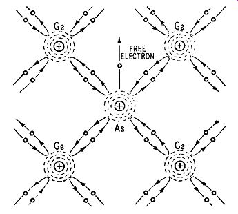
Fig. 1.6. Illustrating covalent bonds in the neighborhood of an atom of
a Group V element introduced into a crystal of pure germanium.
For simplicity, only electrons in the valence rings are shown lattice structure, taking the place of a germanium atom. Now the arsenic atom has 5 electrons in its outermost orbit and 4 of these form covalent bonds with the electrons of neighboring atoms as shown in Fig. 1.6. The remaining (5th) electron is left unattached; it is a free electron which can be made to move through the crystal by an e.m.f., leaving a positively-charged ion.
These added electrons give the crystal much better conductivity than pure germanium and the added element is termed a donor because it gives free electrons to the crystal. Germanium so treated with a Group V element is termed n-type because negatively-charged particles are available to carry current through the crystal. It is significant that the addition of the arsenic or some other Group V element was necessary to give this improvement in conductivity. The added element is often called an impurity and in the language of the chemist it undoubtedly is. However, the word is unfortunate in this context because it suggests that the pentavalent element is unwanted; in fact, it is essential.
When a battery is connected across a crystal of n-type germanium the free electrons are attracted towards the battery positive terminal and repelled from the negative terminal. These forces cause a drift of electrons through the crystal from the negative to the positive terminal: for every electron leaving the crystal to enter the positive terminal another must be liberated from the negative terminal to enter the crystal. The stream of electrons through the crystal constitutes an electric current. If the battery connections are reversed the direction of the current through the crystal also reverses but it does not change in amplitude; that is to say the crystal is a linear conductor. Some part of a transistor is always of n-type material.
ACCEPTOR IMPURITIES
Now suppose an atom of a Group III element such as indium is introduced into a crystal of pure germanium. It enters the lattice structure, taking the place of a germanium atom, and the 3 electrons in the valence ring of the indium atom form covalent bonds with the valence electrons of the neighboring germanium atoms. To make up the number of covalent bonds to four, each indium atom competes with a neighboring germanium atom and may leave this deficient of one electron as shown in Fig. 1. 7. A group of covalent bonds, which is deficient of one electron, behaves in much the same way as a positively-charged particle With a charge equal in magnitude to that of an electron. Such a particle is called a hole in semiconductor theory, and we may say that the introduction
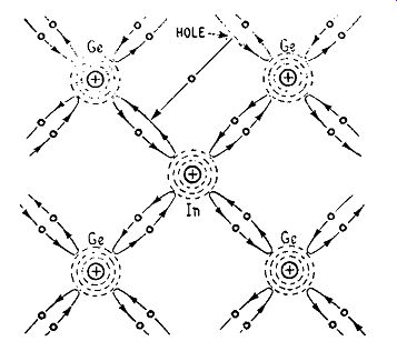
Fig. 1.7. Illustrating covalent bond., in the neighborhood
of an atom of a Group Ill element, introduced into a crystal of pure germanium.
For simplicity, only electrons in the valence rings are shown.
of the Group III impurity gives rise to holes in a crystal of pure germanium. These can carry current through the crystal and, because these current-carriers have a positive charge, germanium treated with a Group III impurity is termed p-type. Such an impurity is termed an acceptor impurity because' it takes electrons from the germanium atoms. Thus the introduction of the Group III element into a crystal lattice of pure germanium also increases the conductivity considerably and, when a battery is connected across a crystal of p-type germanium, a current can flow through it in the following manner.
The holes have an effective positive charge, and are therefore attracted towards the negative terminal of the battery and repulsed by the positive terminal. They therefore drift through the crystal from the positive to the negative terminal. Each time a hole reaches the negative terminal, an electron is emitted from this terminal into the hole in the crystal to neutralize it. At the same time an electron from a covalent bond enters the positive terminal to leave another hole in the crystal. This immediately moves towards the negative terminal, and thus a stream of holes flows through the crystal from the positive to the negative terminal. The battery thus loses a steady stream of electrons from the negative terminal and receives a similar stream at its positive terminal. It may be said that a stream of electrons has passed through the crystal from the negative to the positive terminal. A flow of holes is thus equivalent to a flow of electrons in the opposite direction.
If the battery connections are reversed, the current in the crystal also reverses in direction but has the same amplitude: thus p-type germanium is also a linear conductor.
It is astonishing how small the impurity concentration must be to make germanium suitable for use in transistors. A concentration of 1 part in 10^6 may be too large, and concentrations commonly used are of a few parts in 10^8. A concentration of 1 part in 10^8 increases the conductivity by 16 times. Before such a concentration can be introduced, the germanium must first be purified to such an extent that any impurities still remaining represent concentrations very much less than this. Purification was one of the most difficult processes in the manufacture of transistors.
INTRINSIC AND EXTRINSIC GERMANIUM
If a germanium crystal contains no impurities, the only current carriers present are those produced by thermal breakdown of the covalent bonds. The conducting properties are thus characteristic of pure germanium. Such a crystal is termed an intrinsic semi conductor.
In general, however, germanium crystals contain some trivalent and some pentavalent impurities, i.e. some donors and some acceptors are present. Some free electrons fit into some holes and neutralize them but there are some residual current carriers left.
If these are mainly electrons they are termed majority carriers (the holes being minority carriers), and the material is n-type. If the residual current carriers arc mainly holes, these are majority carriers (the electrons being minority carriers) and the germanium is termed p-type. In an n-type or p-type crystal the impurities arc chiefly responsible for the conduction, and the material is termed an extrinsic semiconductor.
PN JUNCTIONS
As already mentioned, n-type or p-type germanium is a linear conductor, but if a crystal of germanium has n-type conductivity at one end and p-type at the other end, as indicated in Fig. 1.8,
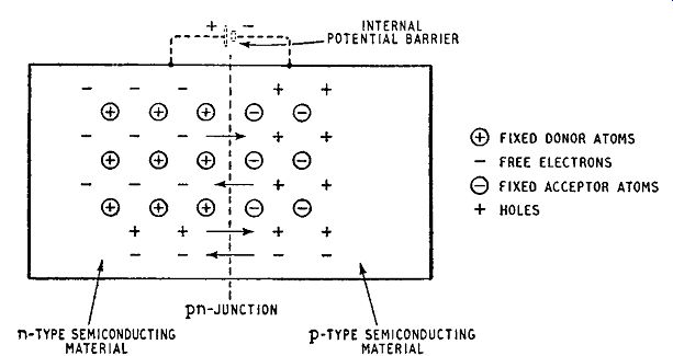
Fig. 1.8. Pattern of fixed and mobile charges in the region of a pn junction
the crystal so produced has asymmetrical conducting properties.
That is to say, the current which flows in the crystal when an e.m.f. is applied between the ends depends on the polarity of the e.m.f., being small when the e.m.f. is in one direction and large when it is reversed. Crystals with such conductive properties have obvious applications as detectors or rectifiers.
It is not possible, however, to produce a structure of this type by placing a crystal of n-type germanium in contact with a crystal of p-type germanium. No matter how well the surfaces to be placed together are planed, or how perfect the contact between the two appears, the asymmetrical conductive properties are not properly obtained. The usual way of achieving a structure of this type is by treating one end of a single crystal of n-type germanium with a Group III impurity so as to offset then-type conductivity at this end and to produce p-type conductivity instead at this point. Alternatively, of course, one end of a p-type crystal could be treated with a Group V impurity to give n-type conductivity at this end. The semiconducting device so obtained is termed a junction diode, and the non-linear conducting properties can be explained in the following way.
Behavior of a pn or op Junction Fig. 1.8 represents the pattern of charges in a crystal containing an np junction. The ringed signs represent charges due to the impurity atoms and are fixed in position in the crystal lattice: the un-ringed signs represent the charges of the free electrons and holes (majority carriers) which arc liberated by the impurities. The n-region contains a few holes and the p-region a few free electrons: these are minority carriers liberated by thermal dissociation of the covalent bonds of the semiconducting element itself.
Even when no external connections arc made to the crystal, there is a tendency, due to diffusion, for the free electrons of then-region to cross the junction into the p-region: similarly the holes in the p-region tend to diffuse into the n-region. However the moment any of these majority carriers cross the junction, the electrical neutrality of the two regions is upset: the n-region loses electrons and gains holes, causing it to become positively charged with respect to the p-region. Thus a potential difference is established across the junction and this discourages further majority carriers from crossing the junction: indeed only the few majority carriers with sufficient energy succeed in crossing. The potential difference is, however, in the right direction to encourage minority carriers to cross the junction and these cross readily in just sufficient numbers to balance the subsequent small flow of majority carriers.
Thus the balance of charge is preserved even though the crystal has a potential barrier across the junction. In Fig. 1.8 the internal potential barrier is represented as an external battery and is shown in dotted lines.
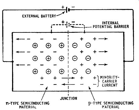
Fig. 1.9. Reverse-bias conditions in a pn junction
Left: Fig. 1.10. Current-voltage relationship for a reverse-biased pn junction
Reverse-bias Conditions
Suppose now an external battery is connected across the junction, the negative terminal being connected to the p-region and the positive terminal to the n-region as shown in Fig. 1.9. This connection gives a reverse-biased junction. The external battery is in parallel with and aiding the fictitious battery, increasing the potential barrier across the junction. Even the majority carriers with the greatest energy now find it almost impossible to cross the junction. On the other hand the minority carriers can cross the junction as easily as before and a steady stream of these flows across.
When the minority carriers cross the junction they are attracted by the battery terminals and can then flow as a normal electric current in a conductor. Thus a current, carried by the minority carriers and known as the reverse current, flows across the junction.
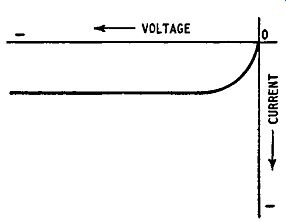
It is a small current because the number of minority carriers is small: it increases as the battery voltage is increased as shown in Fig. 1. 10 but at a reverse voltage of less than 1 volt becomes constant: this is the voltage at which the rate of flow of minority carriers becomes equal to the rate of production of carriers by thermal breakdown of covalent bonds. Increase in the temperature of the crystal produces more minority carriers and an increase in reverse current.
Forward-bias conditions
If the external battery is connected as shown in Fig. 1.11, with the positive terminal connected to the p-region and the negative terminal to the n-region, the junction is said to be forward-biased.
The external battery now opposes and reduces the potential barrier due to the fictitious battery and the majority carriers are now able to cross the junction more readily. A steady flow of majority
Fig. 1.11. Forward-bias conditions in a pn-junction electrons and majority holes can now flow across the junction and these together constitute a considerable current from the external battery. The flow of minority carriers across the junction also continues as in reverse-bias conditions but at a reduced scale and these give rise to a second current also taken from the battery but in the opposite direction to that carried by the majority carriers. Except for very small external battery voltages, however, the minority-carrier current is very small compared with the majority-carrier current and can normally be neglected in comparison with it.
The relationship between current and forward bias voltage is illustrated in Fig. 1.12. The curve has a small slope for small
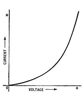
Fig. 1.12. Current-voltage relationship for a forward biased pn junction
voltages because the internal potential barrier discourages movements of majority carriers across the junction. Increase in applied voltage tends to offset the internal barrier and current increases at a greater rate. Further increase in voltage almost completely offsets the barrier and gives a steeply-rising current. The curve is, in fact, closely exponential in form.
Junction Diodes
Junction diodes are very efficient and therefore little heat is generated in them in operation. Such diodes can therefore rectify surprisingly large currents: for example a silicon diode with a junction area less than ½ inch in diameter can supply 50 A at 100 volts. The capacitance between the terminals of a small-area junction is low enough for it to make an efficient detector.
Avalanche Effect
When a pn junction is reverse-biased the current is carried solely by the minority carriers, and at a given temperature the number of minority carriers is fixed. Ideally, therefore, we would expect the reverse current for a pn junction to rise to a saturation value as the voltage is increased from zero and then to remain constant and independent of voltage, as shown in Fig. 1. 10. In practice, when the reverse voltage reaches a particular value which can be 100 volts or more the reverse current increases very sharply as shown in Fig. 1.13, an effect known as breakdown. The effect is reproducible,
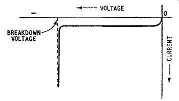
Fig. 1.13. Breakdown in a reverse-biased pn junction
breakdown in a particular junction always occurring at the same value of reverse voltage. This is known as the Avalanche effect and reversed-biased diodes known as Avalanche diodes (sometimes called - perhaps incorrectly- Zener diodes) can be used as the basis of a voltage stabilizer circuit. The junction diodes used for this purpose are usually silicon types and examples of voltage stabilizing circuits employing such diodes are given in Chapter 13.
The explanation of the Avalanche effect is thought to be as follows. The reverse voltage applied to a junction diode establishes an electric field across the junction and minority electrons entering if from the p-region are accelerated to the n-region as illustrated in Fig. 1.9. When this field exceeds a certain value some of these electrons collide with valence electrons of the atoms fixed in the crystal lattice and liberate them, thus creating further hole-electron pairs. Some new carriers are themselves accelerated by the electric field due to the reverse bias and in turn collide with other atoms, liberating still further holes and electrons. In this way the number of current carriers increased very rapidly: the process is, in fact, regenerative. This multiplication in the number of current carriers produces the sharp increase in reverse current shown in Fig. 1.13. Once the breakdown voltage is exceeded, a very large reverse current can flow and unless precautions are taken to limit this current the junction can be damaged by the heat generated in it.
Voltage stabilizing circuits using Avalanche diodes must therefore include protective measures to avoid damage due to this cause.
Zener Effect
Some reverse-biased junction diodes exhibit breakdown at a very low voltage, say below 5 volts. In such examples breakdown is thought to be due, not to Avalanche effect, but to Zener effect which does not involve ionization by collision. Zener breakdown is attributed to spontaneous generation of hole-electron pairs within the junction region from the inner electron shells.
Normally this region is carrier-free but the intense field established across the region by the reverse bias can produce carriers which are then accelerated away from the junction by the field, so producing a reverse current.
Capacitance of a Junction Diode
As pointed out above, the application of reverse bias to a pn junction discourages majority carriers from crossing the junction, and tends to produce a structure in which the carriers are separated by a relatively carrier-free region as suggested in Fig. 1.9. Such a structure is similar to that of a charged capacitor and, in fact, a reverse-biased junction diode has the nature of a capacitance shunted by a high resistance. The value of the capacitance is dependent on the reverse bias voltage and can be varied over wide ...
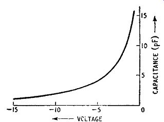
Fig. 1.14. Typical capacitance voltage characteristic for a reverse biased
pn junction
... limits by alteration in the bias voltage. This is illustrated in the curve of Fig. 1.14: the capacitance varies with the voltage according to a law of the type:
c~ kv^-1/n
... where k is a constant and n is between 2 and 3. When n is 2 the capacitance is inversely proportional to the square root of the voltage. A voltage-sensitive capacitance such as this has a number of useful applications: it can be used as a frequency modulator, as a means of remote tuning in receivers or for a.f.c. purposes in receivers. An example of one of these applications of the reverse biased junction diode is given in Chapter 13.
Use of junction diode for voltage reference
The breakdown voltage of a reverse-biased junction diode can be placed within the range of a few volts to several hundred volts but for stabilizer and voltage reference applications it is unusual to employ a diode with a breakdown voltage exceeding a few tens of volts. Some of the reasons for this are given below.
Firstly the breakdown voltage varies with temperature, the coefficient of variation being negative for diodes with breakdown voltages less than approximately 5.3 volts and positive for diodes with breakdown voltages exceeding approximately 6.0 volts.
Diodes with breakdown voltages between these two limits have very small coefficients of variation and arc thus ·well suited for use in voltage stabilizers. However for voltage reference purposes the slope resistance of the breakdown characteristic must be very small and the slope is less for diodes with breakdown voltages exceeding 6 volts than for those with lower breakdown voltages.
Where variations in temperature are likely to occur it is probably best to use a diode with a breakdown voltage between 5.3 and 6.0 volts for voltage reference purposes but if means are available for stabilizing the temperature it is probably better to use a diode with a higher breakdown voltage to obtain a lower slope resistance.
Diodes with breakdown voltages around 6.8 volts have a temperature coefficient (2.5 m V / deg C) which matches that of transistors; this can be useful in designing stabilized power supplies, Voltage reference diodes are usually marketed with preferred values of breakdown voltage (4.7V, 5.6V, 5.5V etc.) with tolerances of 5 percent or 10 percent.