Introduction
AMPLIFIERS such as oscilloscope Y-amplifiers and video amplifiers are required to handle signals which may have steep, almost vertical edges and may also have long, almost horizontal sections. A signal which has both features is a rectangular pulse and is commonly used in tests of Y-amplifiers and video amplifiers: in fact the amplifiers are usually known as pulse amplifiers.
The ability of an amplifier to -reproduce rapid changes in a signal waveform such as a steep edge is determined by the high frequency response of the amplifier: in fact such amplifiers must have a response good up to the frequency given by
f=1/2t
where t is the rise time of the steepest edge.
If the rise time is 0.1 µ,sec the upper frequency limit is given by
f = 1 / 2 x 0.1 x 10^-6 hz
= 5 Mhz
The ability of an amplifier to reproduce very slow changes in a signal waveform such as an almost horizontal section is determined by the low-frequency response of the amplifier: the longer the section of the waveform, the better must be the low-frequency response of the amplifier to reproduce it without distortion. As a numerical example, an amplifier required to reproduce a 50 hz square wave with less than 2 percent sag in the horizontal sections must have a low-frequency response which is good down to at least 1 hz. Sometimes in fact, pulse amplifiers are d.c. coupled to extend the low-frequency response down to zero frequency.
To summarize the above, we may say that pulse amplifiers are characterized by an extremely wide frequency response: for a video amplifier suitable for the British television standards the useful frequency response extends from very low frequencies up to 3 Mhz.
A statement, such as this, of the steady-state amplitude response of the amplifier does not, however, give complete information about its performance as a pulse amplifier. Pulse signals in general contain a large number of components and it is essential for distortionless reproduction of such signals that the components after amplification should reach the output with the same phase relationship that they had at the input to the amplifier. The shunt capacitance which is inevitable in any amplifier causes the phase of high-frequency components of a complex signal such as a pulse to lag behind that of low-frequency components. Such a lag would be comparatively unimportant in an a.f. amplifier but can seriously degrade the performance of a pulse amplifier by increasing the rise time. Phase response is thus important in pulse amplifiers and for a good performance both the amplitude and the phase response must satisfy certain stringent requirements over the spectrum occupied by the signals to be amplified.
For amplifiers using simple inter-transistor coupling networks such as are likely to be used for pulse amplification there is a mathematical relationship between the amplitude and the phase response and, given one, it is possible to deduce the other. In general the better the amplitude response the better is the phase response also and it is thus possible to ensure an adequate phase response by making the amplitude response of the amplifier sufficiently good.
When a pulse amplifier is designed in this way the amplitude response must satisfy standards far more exacting than if phase response were also under consideration. For example to design a video amplifier with a passband extending to 3 Mhz it may be necessary to make the amplitude response of the amplifier flat within 0.1 dB up to, say, 20 Mhz.
alpha' Cut-off frequency
Most transistor pulse amplifiers can be regarded as simple common emitter RC-coupled amplifiers which have been designed with special attention paid to the low-frequency and the high-frequency response so that the necessary wide bandwidth and phase response are achieved. Let us consider the factors which limit the performance of simple RC-coupled amplifiers at the high-frequency end of the spectrum. The two most important factors are shunt capacitances ( chiefly the input and output capacitances of the transistors) and transit-time effects in the transistors (measured by the alpha cut-off frequency). Usually the second factor predominates and its effect on the frequency response of a common-emitter amplifier can be assessed in the following way.
The alpha cut-off frequency is, by definition, the frequency at which the current gain of a common-base amplifier with a short circuited output circuit falls to 0.707 of its low-frequency value when the input circuit is supplied with constant current. For uniform-base transistors this frequency is unlikely to exceed 20 Mhz and a typical value for transistors intended for r.f. applications is 7 Mhz. Most amplifiers are, however, of the common emitter type and for this circuit arrangement the cut-off frequency (for short-circuited output and constant-current input) is much lower. The way in which the common-emitter (or alpha ') cut-off frequency depends on the common-base (or alpha) cut-off frequency can be deduced in the following way.
The current gain alpha' of a common-emitter amplifier at low frequencies is given by ,
Alpha =-- 1 - Alpha where o:0 is the current amplification factor at low frequencies. In general the current gain is given by , alpha
alpha =- 1 - alpha But o: falls as frequency is raised according to the expression Alpha
alpha =--- 1 +jf/f,. where fa. is the alpha cut-off frequency. Substituting for alpha in the general expression for o:' we have , alpha/(1 + jf/Ja.)
alpha = --'----..;..c.....'--' 1 - alpha 0 / ( I + jf!fa.)
- Alpha + jf!fa.
alpha/ ( 1 - alpha)
1 + jf/(1- alpha)fa.
This may be written I I exo ex=----
+ jf/Ja' where fa.' is the alpha ' cut-off frequency.
From this it follows that fa.' = (l - exo)f,.
A typical uniform-base transistor for r.f. applications with ex0
= 0·98 and fa = 7 Mhz has a value off a.' given by fa.' = (l - exo)fry_
= (1 - 0.98) X 7 Mhz
= 140 khz
A higher effective value of fa' could be obtained, at the expense of gain, by the use of negative feedback but the performance of uniform-base alloy junction transistors is in general not good enough for most pulse amplifiers, and drift transistors are preferred.
The performance of a drift transistor as a pulse amplifier is better measured by the frequency f_1. As mentioned on page 35, this is the frequency at which the real part of the current amplification factor has fallen to one half its low-frequency value. This frequency is a most useful criterion of performance because it is also the frequency at which the current gain alpha ' of the common emitter amplifier has fallen to unity; it therefore gives the gain bandwidth product for the common-emitter amplifier and a typical value for j 1 is 70 Mhz. Thus at 35 Mhz, (1 1/2) alpha ' is 2 and at 7 Mhz alpha ' is 10. If an ex' of 35 is required, the highest working frequency of the transistor is 2 Mhz.
In practice simple pulse amplifiers such as those implied in the preceding sentences arc unlikely to be used. This is because the parameters of transistors of the same type inevitably have a spread and it is difficult to construct two or more amplifiers with a similar performance without careful selection of transistors. To minimize this difficulty negative feedback is used.
Use of Negative Feedback
This has a number of important advantages: (a) It extends the passband.
(b) It makes the frequency response and the gain of the amplifier less dependent on the transistor parameters. In fact with a great degree of feedback the gain and the frequency response are to a large extent determined by the constants of a passive network, i.e. the feedback loop. Thus the performance of the amplifier can be predetermined and it is possible to replace the transistors by others with slightly different parameters without significant effect on amplifier performance. It is also possible to manufacture a number of amplifiers all with the same performance within close limits.
(c) By choosing a suitable method of applying feedback the input and output resistances can be made high or low as desired. The precise connections used depend on whether a voltage or a current amplifier is required.
These advantages are not obtained without cost: the application of negative feedback reduces the gain of the amplifier. The way in which negative feedback extends frequency response at the expense of gain is illustrated in Fig. 9.1. The upper frequency
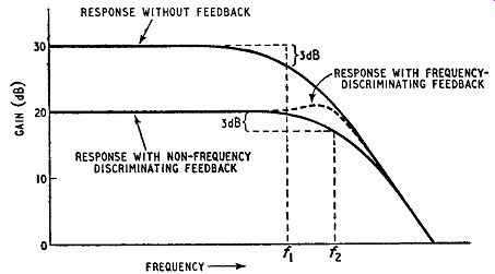
Fig. 9.1. Effect of negative feedback on the frequency response of an amplifier
response curve is that of an amplifier without feedback and is 3 dB down
at the frequency f 1, which can be taken as the upper limit of the passband.
When feedback is applied, the gain falls at all frequencies but the fall
is greater at low that at high frequencies and the new 3-dB loss point is
at f 2 representing a considerable extension of the passband. If the negative
feedback circuit is so designed that the feedback voltage or current becomes
less as frequency rises it is possible to achieve an even greater extension
of the frequency response as suggested by the dotted lines. This, however,
is usually accompanied by an increase in phase distortion and consequent
deterioration in pulse response and it is probably better to adhere to the
aperiodic feedback represented by the solid curve.
Sometimes it happens that the degree of negative feedback required to give the desired passband is so great that the gain of the amplifier is reduced below the wanted value. It is then necessary to add one or more stages to the amplifier to achieve the required passband and gain. This is an illustration of the general theorem quoted above that the gain-bandwidth product for a particular amplifier is unaffected by feedback. If the effect of feedback is to increase the passband by a factor n, then the low-frequency gain of the amplifier is reduced by the factor n. Thus a gain reduction of 6 dB is accompanied by a doubling of the passband. In designing an amplifier to have a particular bandwidth and gain sufficient stages must be included to give at least this value of gain bandwidth product.
If a considerable extension of passband is wanted, a considerable degree of feedback must be used. It is not easy to apply a considerable degree of negative feedback to an amplifier because there is a tendency to produce instability at frequencies near the extremes of the passband. This may take the form of oscillation or a sharp peak in the frequency response curve. Great care in design is essential to avoid these effects. One of the methods used to avoid such effects in a multi-stage amplifier is to employ a number of independent feedback loops, each embracing only two transistor stages of amplification. A similar technique is employed in pulse amplifiers using valves.
Some of the methods of applying negative feedback to two-stage voltage and current amplifiers have been described in Chapter 7 but their application to pulse amplification will now be described in more detail.
Use of Direct Coupling
To obtain a good performance from a pulse amplifier at low frequencies it is advantageous to eliminate coupling capacitors as far as possible because these inevitably introduce attenuation and phase shift at low frequencies. Although negative feedback can be used to reduce these effects, the phase shift limits the degree of feedback which can be employed without instability. Direct coupling is thus attractive not only because it provides a zero- frequency response but also because it eliminates phase shift and enables large degrees of feedback to be used without danger of instability. However, because of the phase shifts present near the upper limit of the passband it is usual to arrange that feedback loops embrace only two cascaded stages.
The use of direct coupling in a transistor amplifier introduces another difficulty. We have already seen in Chapter 6 that the leakage current in a common-emitter stage can vary considerably with change in ambient temperature and unless precautions are taken to stabilize d.c. conditions the current can alter by as much as 2 mA for a 30° C change in temperature. By use of stabilizing circuits this current change can be reduced by a factor of, say, 10 to 0.2 mA. If such a current is fed directly to another transistor with a current gain of 50, the collector current of this second stage will vary by 10 mA. Such large variations are clearly impossible in a small-signal amplifier in which the second stage may require a mean current of only 1 mA. If direct coupling is to be used, therefore, the amplifier must include some method of stabilizing the no-signal collector current of the second transistor. One method is to limit the zero-frequency gain of the amplifier to a very low value such as 2 by means of direct-coupled feedback. If a larger value of signal frequency gain is required this means that the direct coupling is no longer of use in extending the frequency response to zero frequency although it still enables the coupling capacitor to be omitted and facilitates the application of signal-frequency feedback.
Current Pulse Amplifier
As an illustration of the application of these principles we will consider the design of a current amplifier to have a gain of 100 (40 dB). Two cascaded stages are all that is necessary because without feedback two typical common-emitter amplifiers could provide a current gain of 2,500 (i.e., 50 per transistor). If this is reduced to 100 by negative feedback, the gain reduction factor is 1/25 which represents 28 dB of feedback. The input resistance, output resistance, gain and frequency response of an amplifier with such a large degree of feedback would be almost independent of the transistor parameters except near the cut-off frequency.
The amplifier can take the form of a direct-coupled version of Fig. 7.5 in which feedback is applied via the resistors Rb and Re.
Provided the gain of the transistors is high enough the gain of such an amplifier is given by (Re+ Rb){R6 with little error. If Rb is large compared with Re the gain is given by Rb/Re. To give the required d.c. gain of 2, Rb must be equal to Re. These resistors cannot be small otherwise the shunting effect of Rb on the input of the first transistor becomes serious. On the other hand Re cannot be very large otherwise an abnormally-large supply voltage is necessary to give the required I mA in Re. A suitable compromise
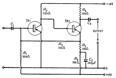
Fig. 9.2. A two-stage current amplifier with negative feedback value for
Rb and Re is 10 k-O. Even with this value of Re a supply voltage exceeding
20 volts is required because the collector resistance for the second transistor
(which is effectively the output resistance of the amplifier) can hardly
be less than 10 k-O and this also carries the 1 mA current of the second
transistor.
To obtain the required zero-frequency gain Rb and Re should both be 10 k-O: to obtain the required signal-frequency gain Rb/Re must equal 100 and if Rb is 10 k-O, Re must be 100 ohms. Both requirements are satisfied if Re is composed of a 10-k-O resistor and a 100-ohm resistor in series, the larger resistor being shunted by a large capacitor to eliminate signal-frequency feedback.
The circuit diagram of the current pulse amplifier thus designed is given in Fig. 9.2 in which all component values are shown. A 27-volt supply is used and the emitter of the first transistor is returned directly to a tapping point on this supply. Any resistance included at this point, whether decoupled or not, would reduce the effectiveness of the d.c. stabilizing circuit.
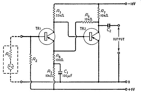
Fig. 9.3. A two-stage voltage amplifier with negative feedback The amplifier
gives the required gain of 100 ( 40 dB) up to a frequency of say 11/20. By
sacrificing gain, however, the response can be maintained up to a higher
frequency: for example by making R2 1 k-O and R5 200 ohms the gain is reduced
to approximately 10 (20 dB) but is maintained up to nearly 1 1/2. A further
improvement in frequency response is possible by making the feedback frequency-dependent
as suggested earlier: this is possible by including an inductor in series
with Ra. The inductance should be so chosen that its reactance becomes appreciable
compared with Ra at a frequency of approximately 1 1/2. The low-frequency
response is determined by capacitor C2 and can be extended as low as desired
by making C2 large enough.
The feedback circuit substantially increases the output resistance of the second transistor and the output impedance of the amplifier is nearly equal to R4, i.e. 10 k-O. The input resistance of the first transistor is reduced by the feedback to around 100 ohms. These are the values of input and output resistance over most of the amplifier passband and the ratio of input to output resistance is very small (1/100) as required in a current amplifier. As frequency approaches the upper limit of the passband the feedback becomes less effective causing the input resistance to rise and the output resistance to fall.
Voltage Pulse Amplifier
From the fundamental circuit for a voltage amplifier given in Fig. 7.6 it is possible to develop a pulse amplifier giving a gain of 40 dB over a wide frequency range. Direct coupling can be used between the transistors and this necessitates a d.c.-stabilizing feed back circuit analogous to that used in the current amplifier described previously. The circuit diagram for such a voltage amplifier is given in Fig. 9.3.
The feedback components are R4, R5, R6 and C1 and these give a zero-frequency gain equal to (R4 +Rs+ R6 )/(R4 + R5), i.e. approximately 2 for the component values quoted on the diagram.
The signal-frequency gain is equal to R6/R4 which is equal to the required value of 100. The high value of Rs necessitates a 27-volt supply which must be tapped to provide an emitter potential for the second transistor. The tapping point is also used to provide the first transistor with a suitable base potential via a potential divider one arm of which is provided by the resistance of the signal source.
To give the first transistor suitable operating conditions the signal source should have a resistance less than 1 k-O. The type of negative feedback used in this amplifier gives a high input resistance (approximately 100 k-O) and a low output resistance (approximately 200 ohms) as required in a voltage amplifier.
The passband obtainable from such an amplifier is slightly better than that of the current amplifier.