AMAZON multi-meters discounts AMAZON oscilloscope discounts
Almost every semiconductor device, such as a transistor, that is suitable
for linear operation can also be used in nonlinear circuits. Nonlinear refers
to the fact that the output of the device is not directly proportional to the
input. For example, in a simple circuit using a transistor as a switch, the
transistor will be either on or off ( like a relay). That is, it is either
conducting heavily, or it is cut off. When there is no base current, the transistor
will be turned off. When there is base current, the transistor will be turned
on and an increase in base current will not turn it on further.
The advent of transistors provided a great step in the development of computers. Transistor switches now replace slow relays and hot, bulky, unreliable vacuum tubes. When applied to transistors and, for that matter, vacuum tubes, the word "nonlinear" can be used inter changeably with "large signal." In linear operation, a small signal input results in minimum distortion and, therefore, linear operation, whereas under large-signal conditions a large input signal overdrives the input circuit, causing distortion in the output and, therefore, nonlinear operation. It is the purpose of this section to show that nonlinear circuits can be put to good use. Switching transistors in computers are operated as nonlinear amplifiers, but transistors in hi-fi sets should be operated as linear amplifiers.
TRANSISTOR SWITCHES
The easiest way to understand the operation of a transistor switch is to compare it with a toggle switch. A toggle switch can be said to be either on or off. A transistor operating in a switching circuit is also designed to be either on or off. Consider Fig. 1A in which a resistor has been placed in series with a toggle switch. The input signal opens and closes the switch. The output depends on the position of the switch.
If the switch is open, the output is connected to the positive supply through resistor R1; if the switch is closed, the output lead is shorted directly to ground; and if R2 has the same value as R1, the output voltage will be 5V when the switch is open and 0V when the switch is closed.
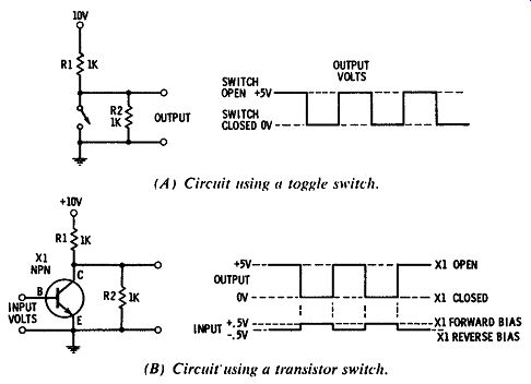
Fig. 1. Switching circuits.
As you will recall from previous sections, the resistance of a transistor may be controlled by the amount of emitter current allowed to flow. When no emitter current flows, the transistor exhibits a very high resistance, or almost an open circuit from collector to emitter. When heavy emitter current flows, the transistor will be a very low resistance, or almost a short circuit. It thus can be used as a switch and will be open or closed, depending on the bias applied to the emitter junction.
In Fig. 1B a transistor is substituted for the switch in Fig. 1A. The transistor switch is open when the emitter junction is reverse biased. The collector current is cut off whenever the emitter junction is reverse-biased. When the emitter junction is heavily forward-biased, the transistor becomes a very low resistance. This condition is referred to as saturation and means that the transistor is conducting just as heavily as possible. A further increase in forward bias on a saturated transistor would result in no increase in emitter-to-collector current.
Further increase in the forward bias of a saturated transistor may destroy the transistor by burning out the emitter-base junction. Because of the gain of the transistor, the input voltage in Fig. 1B need furnish only 0.5V input to saturate the transistor. Thus, a switching transistor is one used in either of two states-saturation or cutoff. When the transistor is saturated, the switch is closed and the collector or output lead is equivalent to being connected to the emitter. When transistor X1 is reverse-biased, no output is present across resistor R2; transistor X1 is at cutoff and the collector is separated from the emitter by an open circuit. There is now a 5V output across resistor R1.
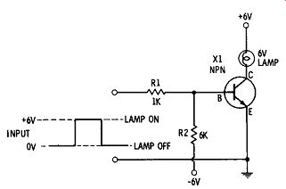
Fig. 2. Transistor lamp driver.
Fig. 2 shows a switching circuit used for turning on an indicator lamp. When the transistor is on, the collector is effectively shorted to the emitter, and the lamp is connected directly across the supply and is lighted. When the transistor is open, or off, the indicator lamp will not be connected to the negative of the supply, but will be floating and the light will be off. The lamp acts as the load resistor for the transistor.
When the input is at 0-V, the transistor is held at cutoff, since the base of X1 will be connected through resistor R2 to the negative 6V supply.
The R1-R2 voltage divider is used to ensure that the emitter junction is reverse-biased, rather than depending on zero bias to keep the transistor at cutoff. Although a transistor will not switch with zero volts on the base, there are many types that are not completely cut off if there is less than .5V of reverse bias. When the input voltage goes to +6V, the voltage at the base becomes positive and the emitter junction is heavily forward-biased. The transistor then saturates, causing the lamp to light.
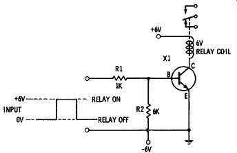
Fig. 3. Transistor used to operate a relay.
Fig. 3 shows a circuit in which a relay is used as the load for a switching transistor. A very small current at the input of the transistor can be used to turn on a high-current relay. This is possible because the transistor provides current amplification. For example, it might take only 10 milliamps to turn the transistor on and 100 milliamps to turn the relay on. Using the circuit in Fig. 2 and a transistor switch witl). a current gain of 10, the relay can be turned on with 10 milliamps.
TRANSISTOR GATES
You will recall that Section 2 provided an introduction to AND OR gates and diode logic. Gates may also be constructed with transistors as the active elements. Fig. 4 shows a two-input AND gate using transistors connected in an emitter-follower configuration. Both transistors are biased to full conduction, the current being supplied through resistors R2 and R4. The output voltage remains at -6V until both X1 and X2 are cut off by the application of +6V at signal inputs A and B. Fig. 5 shows a transistor OR gate. In this case, current sup plied through resistors R3 and R4 maintains both transistors at cutoff.
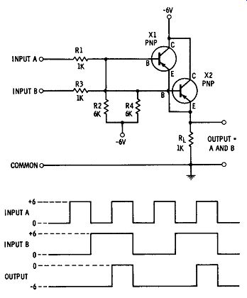
fig. 4. Emitter-follower AND gate.
When either transistor is turned on, the output rises. The output is 0V when both inputs are 0V. These circuits will function as AND, and OR gates, but they are neither the easiest nor the most economical to work with. First, it is easy to see that they require more expensive components than the diode gates mentioned in Section 2. Second, notice that the output voltage levels of Fig. 4 ( -6, 0) are different from the input levels (0, +6) of Fig. 5. This makes it impossible to cascade two such stages without using a level-changing circuit between the two gates.
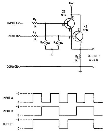
Fig. 5. Emitter-follower OR gate.
Figs. 4 and 5 do, however, serve to introduce the idea of transistor gates.
In practice, gates like those shown in Fig. 6 are used. It is desirable to use transistors rather than diode gates because of the amplification feature. When passive diode gates are used, the output pulses degenerate and lose sharpness after passing through a few gates. This does not happen when transistors are used, because the pulses are re-amplified in each gate. However, each time a common-emitter transistor is used, there is a phase inversion. This means the output is opposite, or inverted, from that at the input. The waveshapes in Fig. 6C show this inversion or negation. The dot ( •) means AND. Thus A • B is read as "A and B." A plus ( +) means OR. Thus A+ B is read as "A or B." The bar over a group means NOT or that the letter or group is to be inverted. Thus, A • B is read as NOT A and B. Figs. 6A and 6B are NOT AND gates. That is, they are AND gates where the AND function is inverted. One gate uses transistors and resistors; the other uses diodes, transistors, and resistors.
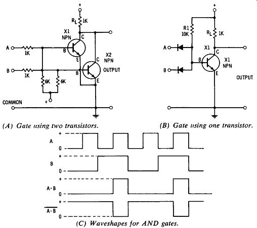
Fig. 6. AND gates.
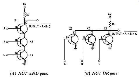
Fig. 7. Typical transistor gate circuits.
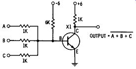
Fig. 7C. Another typical NOT OR gate circuit.
(A) Block diagram of a gate and inverter.
(B) Schematic diagram of a gate and inverter.
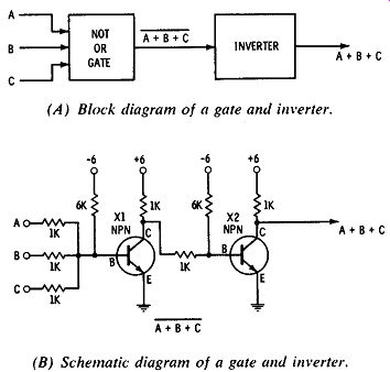
Fig. 8. Inversion of NOT OR function.
Other common gates are shown in Fig. 7. Fig. 7 A is a NOT AND gate. All three transistors must be turned on in order to make the output fall to zero. Fig. 7B is a NOT OR gate. Turning on any one of the three transistors will short the output to ground. A very popular NOT OR gate is shown in Fig. 7C. It is commonly called a NOR circuit. Its popularity is derived from the fact that it uses only one transistor and no diodes. Since resistors are relatively inexpensive, it is an economical circuit. It is well to note that the bar, or NOT, can be removed from any of these logic gates by merely feeding the output through another inverter (Fig. 8A). A schematic diagram of the NOT OR gate and the inverting stage is shown in Fig. 8B.
TRANSISTOR MULTIVIBRATORS
A transistor multivibrator is a square-wave oscillator made up of two transistor switches that are alternately turned on and off. When one transistor is on, the other transistor is off, and vice versa.
Astable Multivibrator
There are three basic variations of the multivibrator-the astable, bistable, and monostable. A typical detailed schematic is shown in Fig. 9 of a multivibrator that operates at approximately 30 khz. X1 and X2 are the two transistor switches. Notice that the output from the collector of X 1 is coupled through C1 to the base of X2, and the output from the collector of X2 is connected through C2 to the base of X1 . The purpose of this arrangement is to provide feedback to keep the device oscillating. When X1 turns on, the output signal is fed back to the base of transistor X2 and turns it off. When X2 turns on, its output signal turns X1 off.
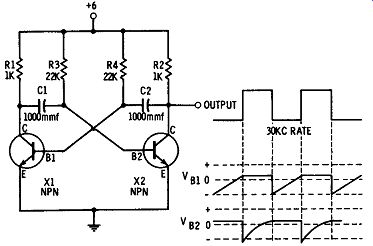
Fig. 9. Astable multivibrator.
Let us take a detailed look at what happens in a multivibrator. To begin the oscillating cycle, some inequality in the transistor switches causes one to conduct more than the other. Suppose X1 has just turned on; this means the collector potential went toward ground. This hap pens so fast that C1 does not have a chance to charge up; and the entire negative change appears across R3, which reverse-biases X2, thus cutting it off. X2 stays off and X1 stays on until C1 charges to the point where X2 is no longer reverse-biased. When this happens, X2 begins to conduct and its collector potential starts toward ground. This feeds a negative pulse through C2 to the base of X1 , turning it off. In a like manner, X 1 remains off until C2 charges completely. The frequency of oscillation is determined by the resistance and capacitance values because they determine the charge and discharge time. The output of this multivibrator is a series of pulses on each collector.
The waveshapes in Fig. 9 illustrate how the oscillations are maintained. Only one switch ( either X1 or X2) is on at a time. While one transistor is on, the other one is off. The off transistor remains off until the capacitor in the base circuit charges to the point where the emitter junction is no longer reverse-biased. Then when this transistor begins to conduct, it in turn turns off the other transistor, and the entire cycle is repeated. Multivibrators are used in all kinds of electronic equipment-particularly in timing circuits, where the output pulses are used to synchronize the operation of other circuits.
Bistable Multivibrators
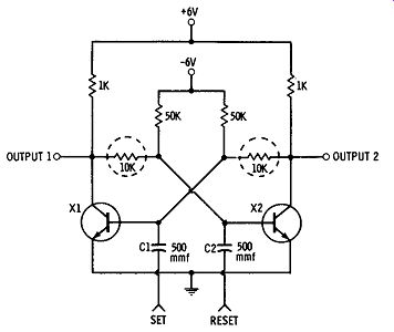
Fig. 10. Bistable multi vibrator.
Once the basic multivibrator circuit is understood, a few simple alterations produce some interesting and useful circuits. The multi vibrator circuit just discussed is a free-running type; that is, it is not stable in either of two states. It is not stable because the feedback coupling from one switch to the other is capacitive and a capacitor can transfer only voltage and current changes. Thus the circuit keeps switching back and forth. By replacing the capacitor with a resistor (Fig. 10), the multivibrator can be made into what is known as a bistable multivibrator. This means that it is stable with either side con ducting. However, by pulsing the circuit in the proper way, it can be made to change from one side to the other. This circuit is also known as a flip-flop.
If X1 is on, X2 will be off and the flip-flop will remain in this state until a pulse is entered, which starts the process discussed for the free running multivibrator. A pulse on the set terminal will turn on transistor X 1 and turn off transistor X2. A pulse on the reset line will cause the bistable to flip, turning on transistor X2 and turning off transistor X1.
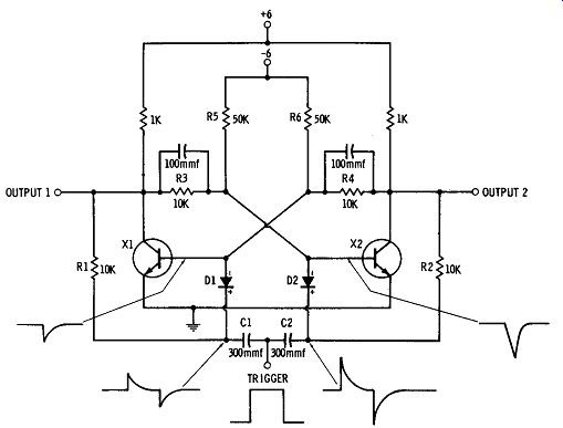
Fig. 11. Triggered flip-flop.
When its state changes, the multivibrator remains in that state until another pulse comes along that will again change its state. Fig. 11 shows a practical triggered flip-flop circuit. In this circuit a trigger pulse will cause a change of state, regardless of the present condition. R1-R2, C1-C2. and D1-D2 make up a "steering" network that directs the pulse to the proper transistor. A large negative pulse is fed to the on transistor, causing it to cut off; as a result, the device flips to the other state. Two capacitors across the feedback resistors (R3 and R4) speed up the switching time by providing an easy path for the high-frequency portions of the pulses. They are known as commutating capacitors be cause they help to speed the commutation of the flip-flop from one state to the other.
A pulse introduced at the trigger lead will be differentiated by capacitors C1 and C2 (Fig. 12). This results in a positive and a
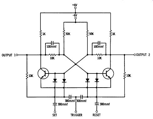
Fig. 12. Set-reset trigger flip-flop.
negative spike. The two diodes permit only the negative spike to reach the bases. Suppose that when this happens, transistor X2 is conducting and transistor X1 is off. When X2 is on, its collector is at zero volts.
This means that R4 and R6 form a voltage divider between - 6V and 0V, thus placing the base of X1 at some positive voltage that keeps it cut off. The negative pulse that reaches the base of X1 is not large enough to cause an effect. The pulse presented to the base of X2, however, is large enough to cut it off. When X2 cuts off, feedback to X1 is such that it is turned on. After the capacitors have charged and discharged, the circuit remains in the state where X1 is conducting and X2 is off. Fig. 12 displays the schematic of a flip-flop that contains both trigger and set-reset capabilities. This multivibrator contains both features of the two previous bistable units.
Monostable Multivibrators
Another circuit in the multivibrator family is called the monostable multivibrator. We have discussed the astable multivibrator and the bistable multivibrator. The monostable multivibrator is one which is stable in only one mode rather than both. This means that when you trigger a monostable, it will change states and then revert to the stable state. It is not free-running, but neither is it bistable; it returns to its original state. As a result, the monostable multivibrator becomes an extremely useful single-pulse generator. Again, this function is accomplished by merely adjusting the feedback circuit to the bases of the two transistors in the basic multivibrator. By having a capacitor in one feedback line and a resistor in the other feedback line, the device will be stable in one state and unstable in the other.
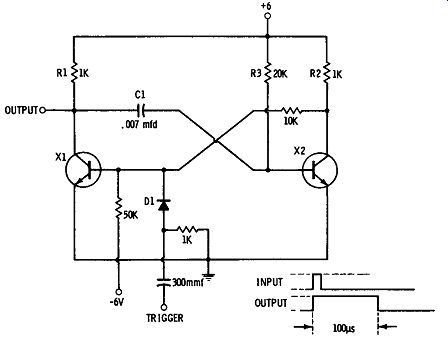
Fig. 13. Monostable multivibrator.
Fig. 13 shows a circuit for a 100 µsec multivibrator. Assume transistor X1 is on and transistor X2 is off. The input trigger circuit is such that an incoming positive pulse will turn X1 off. This will turn X2 on, which tends to hold X1 off. X2 will stay on only until C1 has discharged. Thus the size of C1 and R3 determines the width of the output pulse. As C1 discharges, transistor X2 turns off again, and this action turns X1 back on. The device will settle back to its original position, with the result that the multivibrator action produces an output pulse having a different width from that of the input pulse. The monostable multivibrator is often used as a pulse stretcher. Every time it receives an input pulse, it produces an output pulse having a width that is determined by the time constant of the circuit.
COUNTERS
The bistable multivibrator is often used as a counting device or a memory element. Each flip-flop can count up to two. We shall see shortly that if you consider one output, the number of output pulses will be half the number of input trigger pulses. By using a number of flip-flops, the circuit can be made to count as high as desired by two's.
This system of counting by two's is called the "binary" system. Remember that in the decimal system we count by ten's. Electronic counters use the binary system simply because a two-state device (bistable) is a lot easier to build than a ten-state device. The flip-flop can also be used as a memory device, because if its state is changed, the flip-flop will remember this change until it is changed back. If a flip-flop is used as a temporary memory in a computer system, the computer can come back much later and look at the flip-flop and see that its state was changed.
Fig. 14 shows how a flip-flop divides by two. It takes two input pulses to get one complete output pulse. The "0" and "1" are merely a convenient way of indicating that the transistor switches are on or off. For every two input pulses, the flip-flop will be back to where it was in the beginning. If we put flip-flops following the flip-flop, as is shown in Fig. 15, the output of each flip-flop will be divided by two in the next stage. It can thus be seen that every pulse causes flip-flop 1 to make a transition. Flip-flop 2 makes a transition for every other pulse, flip-flop 3 counts every fourth pulse, and flip-flop 4 makes a
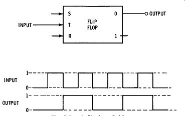
Fig. 14. A flip-flop divider.
transition for every eighth pulse. Using four flip.,-flops in this fashion, one feeding the other, it is possible to count from 1 to 15. After the fifteenth count, all the flip-flops go back to the zero state and the count will start all over again. Each additional flip-flop enables the counter to count twice as high. One flip-flop can count to 2; two can count to 4; three can count to 8; four can count to 16; five can count to 32, etc.
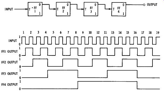
Fig. 15. Four-stage flip-flop divider.
Counters similar to this scheme are used in many places in modern computers. It is with devices very similar to these that all the addition, subtraction, multiplication, and division in computers are accomplished.
Fig. 16. Block diagram of logic elements.
Since many systems exist where hundreds and perhaps even thou sands of flip-flops are used, each with identical schematic diagrams, it would be senseless to draw the entire schematic more than once for the drawings and blueprints of the system. This is particularly true for computer systems. When a drawing is made up for a computer, not only are flip-flops shown as blocks, but so are other logic elements, such as AND gates, OR gates, amplifiers, etc. Each one of these blocks is identical to others of the same type, and therefore nothing would be gained from repeating the schematic. Fig. 16 shows some of the block representations for logic elements. A system diagram made up of these blocks is called a logic diagram. Each block performs a certain logic function. The logic designer is not concerned so much with the circuitry that goes into the blocks as he is with the interconnection of the blocks to perform a certain job. We will see a small example of this shortly.
LOGIC
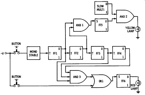
Fig. 17. logic diagram.
If the circuit diagram were drawn out each time one of these devices were used, the result would be so complicated that it would be almost impossible to decipher. Therefore, logic diagrams are used. Consider a simple example of how these devices are used; suppose that an operator of a certain computer pushes two buttons periodically to perform separate operations. Let's call them buttons A and B. We want the computer to keep track of how many times button A is pushed.
After it has been pushed three times, we want a flashing yellow lamp to light on the front panel of the computer. After either button A has been pushed thirteen times or button B has been pushed once, we want a red light to be turned on. Fig. 17 shows a logic diagram for performing these functions. FF1, FF2, FF3, and FF4 make up a counter for keeping track of the number of times button A is pushed. Each time it is pushed, the monostable generates a pulse which is counted. After the operator has pushed the button three times, FF1 and FF2 both have a "one" in the output. This energizes AND-1. Thus, this gate will have an output when the count is 3. FF5 is then set, enabling AND-2, allowing the pulses to get through to the yellow lamp. Since AND-2 will have an output only when the multivibrator is on, the lamp will flash in synchronization with it. The purpose of FF5 is to remember that count "3" has been reached, even after it has passed. When the count for button A is 13, AND-3 will have an output that passes through OR-1, setting FF6 and turning on the red lamp. The red lamp will also be turned on if button B is pushed. The purpose of FF6 is to remember that the "13" count was reached, even after it has been passed. If FF5 and FF6 were not in the diagram, the lamps would stay lighted for only one count. To start all over, a reset pulse would be entered into the reset leads of all FF's.
When it comes to understanding computer operations, the problem is not tied up in the circuitry; it is in understanding the logic. Most circuits are simple, but the way the logic blocks are interconnected is the difficult part. The computer then can be considered as a lot of simple blocks interconnected to perform a complex function. Each of these blocks contains transistor circuitry.