In this Section we will look at selected circuit operations found in the Sony Betamax VCR system and the RCA (VHS) Home Video Recorder system.
RCA VCR CIRCUIT OPERATIONS
We will now look at video recorder circuits found in some model VBT 200 RCA home video recorder systems.
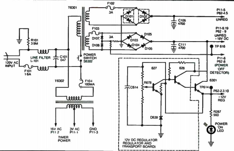
Fig. 10-1. Power supply circuit with +12 volt regulator.
The Power Supply Circuit
The video cassette recorder power supply shown in Fig. 10-1 uses a power transformer (16301) and two bridge-rectifier circuits to develop sources of unregulated 12-volts DC and an unregulated 18 volts DC. A third unfiltered supply, using diodes D107 and D108, produces the "power-off detector" supply. The voltage is fed to the regulator and transport board logic system to sense a power failure and operate the stop solenoid so that the machine is not left in an operating mode in the event that AC power is lost. A second power transformer (T6302) supplies 16 volts AC and 3 volts AC to operate the digital timer.
AC power for the main power transformer (16301) and the timer power transformer is supplied via the AC line with a 1.6 amp fuse. Because of the low power demand of the clock/timer, a separate 100 mA fuse is used to protect the timer power transformer. Other fuses protect the rectifier/filter system and the unregulated 18 volt supply.
The unregulated 12 volt supply output is fed to the regulator and transport board where it encounters some switching. This voltage is also fed to the D-D motor board where it provides input power to operate the three phase inverter that then drives the D-D cylinder motor.
The unregulated 18 volt supply is also fed to the regulator and transport board where it provides power to operate much of the logic circuitry contained on this board as well as the stop solenoid. Also derived from the unregulated 18 volt supply is regulated 12 volt DC which is generated by a series-regulator circuit that utilizes low-level drive circuitry on the R & T board, and a power transistor (TR6301) which is chassis mounted. The regulated 12 volt source appears at the emitter of transistor TR6301 and can be measured at test point TP 614. Also, note that the "power on" indicator (an LED) is powered from the regulated 12 volt source. Thus, from the servicing standpoint, if stop-solenoid action is heard when the VCR power is turned "on" and "off", but the "power-on" indicator does not come "on", this would point to a problem in the regulator circuit. This is because the 18 volt supply powers the stop solenoid and supplies input voltage to the regulator which then drives the "power on" LED. Most of the circuitry in this VCR is powered from the regulated 12 volts power source.
In summation, the power supply circuit provides three voltages to the R & T boards. These voltages are +12 volts unregulated, "power off" indicator voltage, and +18 volts unregulated. These are all directed to the R & T board. A driver circuit on this board supplies bias to the 12 volt regulator transistor (TR6301) which is chassis mounted. Also, associated with plug P61, pin 3 is the regulated output of 12 volts from this board which is fed to the luminance subprocess board via plug P39-5.
Power Supply Service
Tips Because the power supply is the heart of any electronic system, if you have a VCR that is completely inoperative or some functions do not work at all, then check out all power sources for the correct voltage.
If some DC voltages are low or fuses are blown then look for leaky filter capacitors or shorted diodes in the bridge rectifier circuits. Also, be on the alert for shorts or circuit loading from other VCR system circuits. If you suspect shorts in other sections of the VCR, then disconnect each supply voltage lead, one at a time, until the excessive load is located.
Should the +12 volt regulated power source not be correct, measure the +18 volt DC and see if it is correct. N the +18 volt power source is correct then look for component trouble in the 12 volt regulator board.
Chroma Record Circuits (RCA Home VCR)
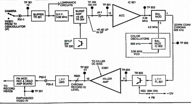
Fig. 10-2. Simplified chroma record block diagram.
The chroma record circuits are separated from the luminance processing as can be seen in Fig. 10-2. Video signal enters the luminance board via P31-1 where it can be observed as 1 volt signal at TP301. This signal passes via the isolating buffer TR 301 and is routed to the luminance and chrominance processing circuitry. Note that the video signal output of buffer TR301 is applied to the 3.58 MHz bandpass filter T308 which separates the chroma component from the luminance signal. The chroma signal then is applied to a stage called the "burst amplifier" which also serves as a chroma amplifier. The designation burst amplifier results from the fact that when the unit is operating in the 2-hour "record mode", the burst receives an additional 6 dB of amplification to accomplish the desired 6-dB burst enhancement function which is part of the VHS standard. In the 4-hour mode of operation, the additional burst boost is not used, and transistor IR 324 only serves as a chroma amplifier stage. Output from the burst amplifier is viewable at test point TP 309. This signal is then routed to the chroma board via interconnecting cables.
Once the signal is on the chroma board, it enters chroma processing IC 801 at pin 13. The scope can be used to view this signal at test point TP 801. Once inside the IC, the chroma signal passes through ACC (automatic chroma control) circuitry which removes any level variations, in the same way as the ACC circuitry does in a color TV receiver. ACC regulated chroma is applied to a balanced modulator which is part of the same IC. The balanced modulator is pin 3 of the IC, and the signal can be seen with the scope at test point TP 803. Also entering the balanced modulator via pin 5 is a 4.2 MHz CW signal generated by beating a 3.58 MHz VXO output CW with 629 kHz rotary CW in a second balanced modulator. The 629 kHz down-converted chroma signal (scope at test point TP 805) emerges from the chip at pin 7.
A low pass filter (C818 and FL801) rejects everything except the 629 kHz chroma signal. Output from this filter (selectable by an electronic switch IR 803 which is "on" during "record") is routed back to IC 801 via pin 9 and can be scoped at TP 804. The signal entering the chip passes through a killer-amplifier stage which is turned "on" and "off" by the color killer circuit. When the VCR is recording a color program, the killer amplifier stage is active and passes a signal via pin 10. This down converted 629 kHz signal can be scoped at TP 802. After passing through the chroma-record level control (R820) and a low level filter (L803 and C807), the down converted 629 kHz chroma is fed back to the luminance board so it can be transferred to the FM modulator record and head amplifier board via plug P35-2. Once on the FM-modulator board, the chroma signal is mixed with luminance in the record amplifier stages.
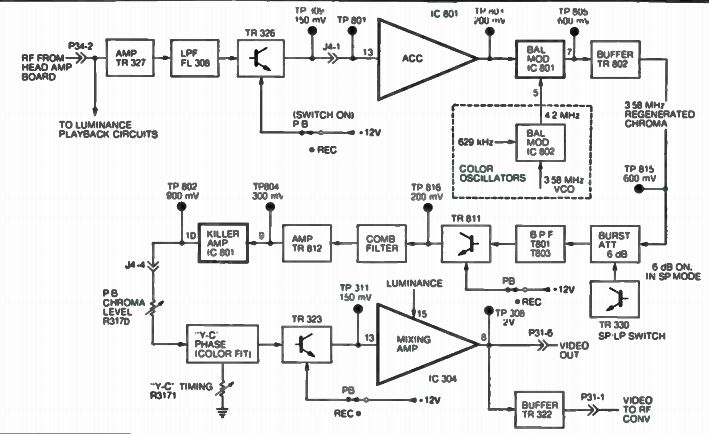
Fig. 10-3. Simplified chroma playback block diagram.
Service Tips
These record/play chroma circuits can be best serviced by using the oscilloscope to trace the signal throughout the various stages and IC's.
Record/Play Circuits (RCA Model VBT-200 VCR)
These Record/Play circuits are used in RCA's model VBT-200 video tape recorders (VCR). As we note in Fig. 10-3 the RF signal (head-amplifier output) is fed to the luminance board via plug P34-2. At this point, the RF signal is directed to the luminance and chroma circuits. Following the chroma signal path, the RF signal drives amplifier transistor IR 327 whose output is applied to the ACC amplifier on the chroma board (via low-pass filter FL 308 and electronic switch transistor IR 326). You may wish to check for this signal at test point TP 309, with the scope.
Once the signal is on the chroma board, it can be scoped at test point TP 801 as the ACC-amplifier input signal to IC 801 pin 13. The ACC amplifier system of IC 801 acts to minimize level changes in the chroma signal that might be caused by different video tape characteristics and/or physical defects in the tape. Output from the ACC amplifier (TP 803) is applied to a balanced modulator which is part of the same chip via pin 3.
Also entering the balanced modulator via pin 5 is a 4.2 MHz CW signal. In playback, the balanced modulator output is the difference between the 629 kHz down-converted chroma and the 4.2 MHz CW signal which is the 3.58 MHz up-converted chroma. Balanced-modulator output is via IC 801 pin 7 and this signal can be seen with the oscilloscope at TP 805. In playback, the 3.58 MHz regenerated chroma signal drives the buffer transistor TR 802 whose output signal can be observed at TP 815.
Up-converted chroma is then fed to TR 807, a two hour/4 hour switchable 6-dB burst-attenuation stage. In the 2-hour mode, burst is attenuated by 6 dB because it was originally boosted by 6 dB during "record". In the 4-hour mode, this stage merely serves as a chroma amplifier. After passing through a 3.58 MHz bandpass filter (T801 through T803), filtered chroma (TR 807 signal) drives a playback comb-filter circuit via an electronic switch transistor TR 811 which is turned "on" during playback. This switch output can be scoped at test point TP 816 when troubleshooting this circuit stage.
The comb filter is a rather sophisticated circuit that utilizes a "1-H delay line" in conjunction with the chroma rotary-phase recording technique to minimize chroma crosstalk in the color video signal. The chroma rotary-phase system is designed to assure that the chroma crosstalk component is always out of phase with the desired signal.
Because of the line-to-line redundancy of the color information in the picture, it is possible, by use of a 1-H delay line, to add the chroma signal from the chroma processing circuit along with the chroma from the previous line (1-H delayed) to obtain twice the amplitude of the chroma and cancel the crosstalk. Obviously, this is a highly simplified explanation of the chroma rotary-phase and the comb-filter circuits. However, for most troubleshooting procedures, this explanation of the circuit operation should suffice.
Chroma from the comb filter drives the amplifier transistor TR 812 whose output signal (TP 804) is fed to pin 9, of IC 801, where it passes through a killer-amplifier stage that enables or defeats the chroma circuits with the presence or absence of a color signal. Output from the killer amplifier emerges from the chip at pin 10 and is then fed to the luminance board via jumper J4. This signal can be viewed with the scope at test point TP 802. Once the chroma signal is back on the luminance board, it passes through the playback level control (R3170) which allows adjustment of the playback chroma amplitude.
The chroma signal is then fed to the "Y-C" phasing circuit. Basically, the "Y-C" phasing circuit consists of phase-shift components in conjunction with the "Y-C" timing control R3171. The purpose of this circuitry is to allow adjustment of luminance/chrominance timing, thus color fit. This network output passes through a playback electronic switch (transistor TR 323) whose output is matrixed with the luminance signal in the mixing amplifier of IC 304. The chroma input signal can be seen with the scope at TP 311. Once the chroma signal is mixed with luminance, it follows the previously described path to the RF modulator or to the external video-output jack.
ZENITH (SONY) BETAMAX VCR SYSTEM
In this section we will be looking at some selected circuits from the Zenith JR 9000 VCR machine. Let's first look at the block diagrams of the overall system operation.
Video Recording Mode
The signal is fed to the tuner and IF board and detected for video and audio signals. The luminance signal routes the video via the Y -FM modulator block. A developed AGC signal automatically regulates the level of the input signal to the modulator.
The video signal is then fed through a 3.58 MHz trap circuit and now becomes the luminance signal. Luminance is then converted to an FM signal by the FM modulator and then fed to the two recording heads.
Referring to Fig. 10-4, we see the video signal is then fed on for chroma processing. The chroma signal system is a "color under" system in which the chroma position of the NTSC video signal is down-converted to 688kHz from 3.58MHz. This is achieved by heterodyning a 4.27MHz signal with the 3.58MHz and using the difference signal 688kHz. This signal is then processed to develop the automatic color control (ACC) and the automatic color killer (ACK) voltages and then coupled to the video head. These record signals are shown in Fig. 10-5.
Both the FM luminance and the down converted 688kHz color signals are combined in the two video heads, which produce the recorded video signal on the tape.
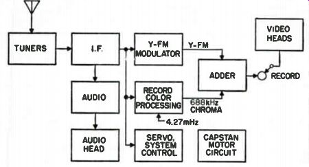
Fig. 10-4. Block diagram of record mode.
The Video signal input to the control circuit on the RS-L board activates the drum servo and pulse generator integrated circuits.
The servo system controls the speed of the head drum only and the pulse system produces switching signals used in switching between the two heads and in switching the 4.2 MHz carrier. The vertical signal which has been separated from the composite video is passed through an integrator network to extract only the vertical sync pulse. The output toggles a flip-flop which divides and shapes the signal into a 30 Hz square wave. This "control" signal is recorded onto the tape. This same signal is processed to control the drum brake; and thus the speed of the Heads.
Video Playback Mode
On playback, the video chroma and control signals are taken from the video heads, then processed and routed out through a RF modulator with an RF output on either channel 3 or 4. Refer to Fig. 10-6 for a simplified block diagram of the playback mode.
The video signal (Y-FM) is picked up by the video heads, sent to the YC-L board where it is amplified, deemphasized, limited, demodulated, and sent to the RF modulator which gives an RF output on either channel 3 or 4.
The chroma signal pickup from the video head is converted back to 3.58 MHz. Any crosstalk or jitter is attenuated and ACC and ACK voltages are developed. The chroma is then added to the luminance signal, coupled to the RF modulator, and then out of the VCR to the TV monitor.
The control track on the tape is picked up by the control head, amplified and sent to a delay circuit and onto the brake circuit. The speed of the head drum is therefore servo controlled by comparison against the playback control signal.
In early model VTRs, the rotational speed of the head drum and the forward speed of the tape past the drum was selected so that between each of the slant video tracks, recorded on the tape, is an unrecorded area. This blank area, called the "guard band" has been necessary in order to reduce cross talk between adjacent tracks during playback. The concept is the same as with the guard band between the tracks on a longitudinal audio recorder.
In the Beta tape system, the guard band between adjacent tracks has been reduced to zero. Two comparatively new techniques are utilized to reduce cross talk. One principle of this technique is based upon the inherent loss of high frequency playback response which occurs when azimuth misalignment exists between the record and playback head gaps.
This phenomenon is well known to most technicians who have made head azimuth adjustments in audio recorders. The angle of both the record and playback head gaps to the recorded track must be the same or high frequency response is lost.
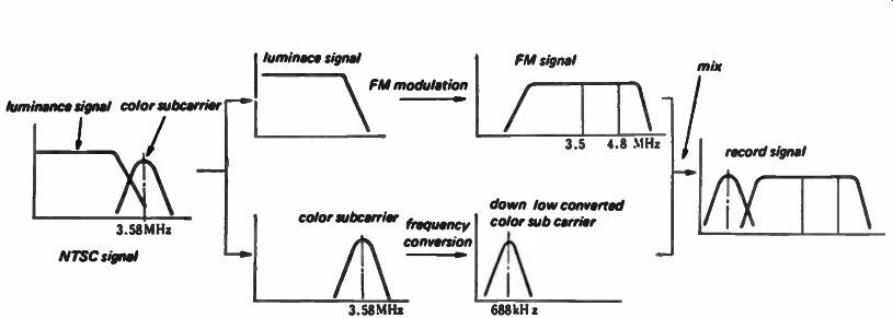
Fig. 10-5. Record signal distribution.
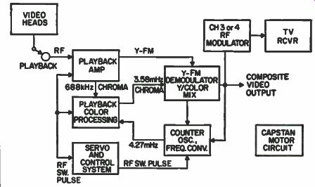
Fig. 10-6. Block diagram of playback mode.
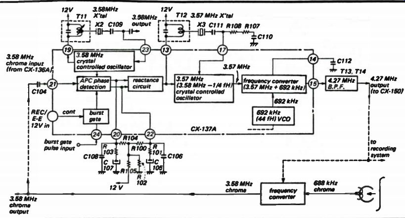
Fig. 10-7. Block diagram of APC circuit.
Since in any two-head, helical scan VCR, the adjacent track on each side of the track being played back, at any given instance, is always a track recorded by the head not in contact with the tape. Thus, cross talk can be attenuated at the relative high luminance FM frequencies by deliberately introducing an azimuth displacement between the two head gaps.
APC Circuit Operation
The APC (automatic phase control) functions only in the playback mode, but not in the record mode.
A block diagram of the APC circuit is shown in Fig. 10-7. It consists of a phase detector, reactance circuit, 3.57 MHz (3.58 MHz - 1/4 fH) crystal controlled oscillator, burst gate circuit which performs phase detection only for the burst signal, and a 3.58 MHz crystal controlled oscillator whose output is used as a phase reference. The reactance circuit is a variable capacitance type and is connected to the 3.57 MHz crystal controlled oscillator to be part of its oscillating time constant. The reactance circuit and the crystal controlled oscillator are interconnected so that the 3.57 MHz oscillator is a voltage controlled crystal oscillator (VCXO). In the record mode the 3.57 MHz oscillator is a stable reference oscillator. In playback the frequency of the VCXO is controlled by the output of the phase detector. The VCXO output is supplied to the frequency converter where it beats against the output of the 692 kHz (44 fH) VCO to produce 4.27 MHz. This 4.27 MHz output is fed to a bandpass filter and supplied to the chroma frequency converters of the record and playback system. The playback 3.58 MHz chroma signal is then fed to the APCV PHASE DETECTOR. The reference signal is supplied by a 3.58 MHz crystal controlled oscillator. The output signal of this oscillator and the burst portion of the two (record and playback) chroma signals are phase compared.
The detector output is filtered in RC filters and fed to the VCXO to control the 3.57 MHz oscillator frequency. Since phase comparison is made only with the burst signal, the burst gate controls the phase detector so that the output of the APC phase detector is supplied only during the burst period. In the record mode, the output of the APC phase detector is blocked by applying the REC/E-to-E+ 12 volts DC to the burst gate as a control voltage in order to stop the operation of the burst gate. This allows the 3.57 MHz VCOX to function as a fixed frequency oscillator in the record mode. In playback, the 688 kHz Chroma signal reproduced by the video heads is at a frequency which is 43.75 times the horizontal sync signal and contains phase instability caused by mechanical jitter. The AFC loop slightly over-corrects this phase instability since the horizontal sync frequency cannot be multiplied by 43.75. The APC loop detects the small phase variations which result from this over correction and develops a DC control voltage which controls the instantaneous frequency (phase) of the 3.75 MHz (3.58 MHz - 1/4 fH) VCXO to compensate.
CX137A IC APC Circuit Checks
For proper voltage at the chip check for +12 volts DC at pin 2 of the chip. Also, check for +8 to +8.5 volts DC at pins 20 and 22 of the IC. If voltage is not correct check components at pins 20 and 22. If components are good then suspect a faulty chip.
For APC loop operation make sure the scope waveforms at pins 4, 5, and 6 are like those shown in the Fig. 10-8 block diagram.
The Chroma Record System
The chroma record system functions as a record ACC (automatic chroma level control), as a color killer, and performs the frequency count-down conversion to 688kHz. The block diagram in Fig. 10-9 illustrates chroma record operation. The video signal is applied to a 3.58 MHz bandpass filter where the chroma signal is separated.
The filter output is supplied to the ACC gain-controlled amplifier.
This circuit is similar to the ACC control range found in a TV receiver.
This amplifier controls the gain to maintain the burst signal at a constant level.
The ACC output is fed to a frequency converter and burst gate circuit.
Also, applied to this circuit is a delayed horizontal sync input. It opens the burst gate at the proper time to allow only the burst through. This burst signal is then coupled to the burst transformer and then to a crystal ringing filter circuit which converts the burst signal to a CW signal. The mean amplitude of this CW signal is proportional to the amplitude of the burst signal. The filtered CW signal is then sent to an amplifier which amplifies it to a level high enough to drive the following ACC detector circuit.
The ACC peak detector detects the CW signal and compares it with the reference voltage to obtain an error voltage. The ACC output level is adjusted by changing the reference voltage. The output voltage is supplied to the ACC gain-controlled amplifier and to the color killer stage via the DC amplifier.
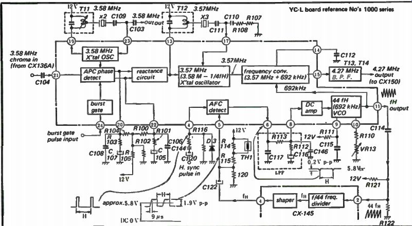
Fig. 10-8. Block diagram of CX137A chip.
The color killer level is automatically set by the setting of the ACC output level, so that the killer actuates when the ACC level drops 1 dB below the reference. The color killer output is applied to the frequency converter. When no color signal is present, the killer cuts off the frequency converter. The color killer output voltage is +4 volts in the chroma mode, and zero in the monochrome mode.
The chroma signal is routed from the ACC control amplifier to the frequency converter. In the frequency converter, which is a balanced modulator, the chroma signal is heterodyned against a 4.27 MHz CW signal supplied to the frequency converter. This provides the sum and difference components of the two input frequencies. These frequencies are about 7.9 MHz and 688 kHz. The output of the frequency converter then goes to a low pass filter which rejects the higher frequency allowing only the 688 kHz signal to pass through.
Chroma Signal System Circuit
After separation from the Luminance, the 3.58 MHz Chroma signal is applied to a frequency converter as was previously stated. Here it is heterodyned with 4.267919 MHz signal. The resultant 688.3774 kHz signal is recorded on the tape. The 4.267919 CW signal is derived in a manner such that it is always phase-locked to the horizontal sync in the incoming video signal. The output signal from a 3.575611 MHz crystal oscillator is beat against the output signal from a 692.307 kHz voltage controlled oscillator, and the VCO is kept phase locked to horizontal sync.
When the two signals heterodyne in the frequency converter, the resultant sum frequency is the 4.267919 CW signal. The 692.307 kHz VCO is kept-phase locked to the incoming "H" sync by dividing down its output frequency to 15.734 kHz in a divided by 44 count-down circuit.
The 15.734 kHz output signal from the countdown circuit is phase-compared against incoming separated H sync in a phase comparator which yields a DC output voltage. The DC output from the phase comparator is applied to the 692.307 kHz VCO as the control voltage. As shown in Fig. 10-10, the 692.307 kHz output frequency is exactly 44 fH. When they heterodyne, the resultant 4.267919 MHz signal is equal to 3.579545 MHz + (44- 1 / 4) fH. This means that the down converted chroma signal has the relationship (44- 1 / 4) fH locked to incoming horizontal sync.
As the result of this relationship, the 688 kHz down-converted chroma signal recorded on the tape retains the same relationship to H sync as did the original 3.58 MHz chroma signal. The carrier phase inverter circuit is driven by a flip-flop output and RF switching pulse. The flip-flop is triggered by the horizontal pulse. The 30 Hz switching pulse is supplied by the RG board. During "A" head field period, the flip-flop is toggled back and forth line-by-line. Then the 30 Hz pulse switches to "B" head and no phase reversals occur because the horizontal pulse cannot change the flip-flops mode.
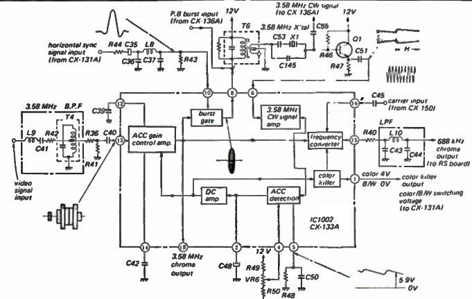
Fig. 10-9. Record chroma signal processing circuit.
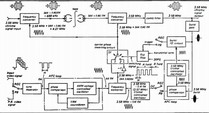
Fig. 10-10. Simplified block diagram of chrome system.
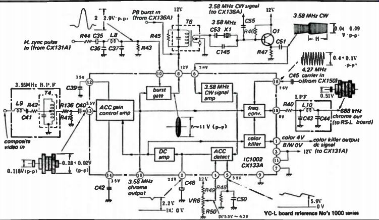
Fig. 10-11. Block diagram of CX133A chip.
CX133A Chroma Processing IC
The type CX133A IC has been specially developed for use in the chroma signal processing circuit of VCR's. This IC encompasses the following seven functional circuits.
• Input for 3.58 MHz chroma ACC gain control amplifier.
• Burst signal gate.
• 3.58 MHz CW (continuous wave) amplifier.
• Detector for ACC drive.
• DC amplifier
• Color-Killer signal generator circuit.
• 3.58 MHz frequency converter into 688 kHz chroma signal.
Troubleshooting Tips
Since these seven circuits are working together, the individual circuits cannot be checked independently. Use the block diagram in Fig. 10-11, which gives all of the correct oscilloscope input and output waveforms along with the correct DC voltages that should be found on pins of this CX133A chip.
Chroma Playback "Chip"
In the chroma playback mode the RF signal is fed from the RF playback amplifier on the RS-L board. This signal contains both the chroma and Y -FM signals. This signal is routed through a low pass filter which rejects the Y-FM signal, extracting only the 688 kHz chroma signal. Refer to Fig. 10-12 for the CX136A chroma playback chip block diagram.
The 688 kHz signal is applied to an ACC gain controlled amplifier.
The DC voltage, obtained by detecting the playback burst signal, is applied to the gain controlled amplifier. A feedback loop thus formed adjusts the gain of the ACC amplifier so that the burst signal level remains constant.
Since separate capacity stage circuits for the ACC detection output are provided for each channel, the ACC loops are independent for each of the two heads and no difference in chroma output level is distinguishable even if a large level difference exists between the two head outputs.
The ACC output signal, 688 kHz, is applied to a frequency converter where it is heterodyned and the difference signal of 3.58 MHz is produced.
The phase of the playback chroma signal is inverted at a 1H rate when the "A" head is playing back. This is restored to continuous phase in the frequency conversion process.
The signal now passes through the 3.58 MHz filter and then to an emitter follower circuit and is coupled to the comb filter, where the cross talk component is removed. The comb filter output is applied to an output amplifier. From the amplifier the signal is fed to the Y/C Mixer.
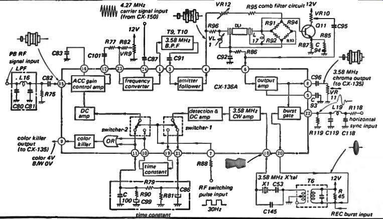
Fig. 10-12. Chroma playback circuit
AGC Control Circuit
A burst gate, using a delayed horizontal signal as the gate control, extracts the burst signal. The extracted burst is supplied to the 3.58 MHz crystal filter. This is the same crystal filter circuit used in the record system. As in recording, the burst signal is converted into a 3.58 MHz CW signal of low level. It is amplified to a high enough level to drive the detector circuit.
The 3.58 MHz signal, whose amplitude is proportional to burst, is detected in the detector circuit whose output is fed to a hold circuit via switcher 1. Separate hold circuits are provided for each of the video heads and switching is done by switchers 1 and 2. Using this method the ACC loops become independent for each channel. This results in no signal level difference, in chroma output for the two combined channels, even if there is a big difference in the chroma output levels of the two heads. The RF switching pulse (30Hz) drives switchers 1 and 2. The output of switcher 2 is amplified in a DC amplifier to drive the ACC gain controlled amplifier.
The filtered outputs of the time constant are also sent to the color killer circuit via an OR gate. The color killer is set to actuate when the ACC detector output voltage drops below the control range of the loops.
The DC voltages at the output of the time constant circuit decrease so that the ACC amplifier gain increases when the chroma signal is low. When this level decreases below the control range of the ACC, the ACC locks out and the voltages of the time constant circuits drop to about 1 volt. The color killer functions when either of the two channels locks out. The output of the color killer is 4 volts DC in the color mode and zero in the monochrome mode.
CX136A IC Circuit Checks and Tips
The CX136A IC is used for playback chroma processing, encompassing the circuits of playback ACC gain control amplifier, playback color killer circuit and frequency converter to convert 688 kHz playback chroma to the 3.58 MHz chroma output signal. Refer to the block diagram (Fig. 10-13) for the correct scope input and output signals along with the proper DC voltages at the pins of the IC. Some troubleshooting symptoms that may be caused by this chip circuit are as follows.
• No color
• Color flicker (ACC does not work)
• Carrier leak and/or Cross talk in color signal
For no color check for 3.58 MHz chroma signal (1.9 volts) at pin 8 of the IC. Is color killer output of about 4 volts DC present at pin 9 of IC? Check the 30 Hz switching pulses present at pin 7 of the chip. Check for a chroma signal of 0.3 volt at pins 9 and 10 of the CX135A chip. If all input signals are near normal but output signals are not and the DC voltages seem to be incorrect then the CX136A chip would be a prime suspect.
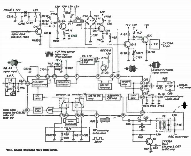
Fig. 10-13. Block diagram of CX136A chroma processor IC.
ZENITH MODEL KR9000 VCR
For normal VCR operation a TV station signal (VHF or UHF) is recorded by the machine and later played back through a television receiver. Thus the input to the KR9000 is at a VHF or UHF frequency, with video chroma and audio modulation.
The Record Mode
Looking at Fig. 10-14, we see the TV input signal appears at the top left of the block diagram. Each input signal is coupled through a splitter, producing two outputs each for VHF and UHF: These tuners operate very similar to tuners in conventional TV receivers.
The output of the tuner(s) is at I.F. or intermediate frequencies in the 41 to 47 MHz bandwidth. The IF signal is processed by circuitry on the IF-4 board, very similar to a TV set operation. The signal is amplified and the three resultant signals developed by detection circuits are the outputs of this IF functional block. One signal is the recovered video signal, which includes both the luminance and chroma information. Another output is the audio signal portion of the program being processed. A third output is an AFC, signal, which is developed by a circuit that senses a change in IF video carrier frequency caused by tuner oscillator drift. This DC voltage is coupled back to the tuner oscillator circuit, resulting in a continuous correction of oscillator drift, locking the oscillator to the correct frequency for the channel signal received.
As the video head revolves during the record process, two magnets on the bottom side pass over fixed coils to create the PG pulses, that are directly related to the speed of the head rotation. These pulses are coupled into the ARS board, where they are compared with a signal developed from the video information, to control and maintain the correct speed of the video head.
The Playback Mode
When the recorded video tape is played back, the heads pick up the information as the tape moves past them. The audio head couples the audio information to the ARS board, for amplification and connection through the CP-3 board to the audio output socket and the RF modulator. Note block diagram of the playback mode in Fig. 10-15.
The control head sends the control track signal to the ARS board where it is compared with the 30 PG pulses from the revolving video head for maintaining the correct speed of the video head.
The video heads track the recorded video signal on the tape and the rotating transformer couples this information to the ARS board. The video signal is composed of the FM luminance and 688 kHz chroma signals, which are amplified and separately coupled to the YC-2 board for further processing. This processing recovers the original luminance frequencies as well as the 3.58 MHz Chroma, which are mixed together to form the normal NTSC composite video output that connects to the CP-3 board and the video output socket as well as to the RF modulator.
The audio and video signals are used to modulate either a channel 3 or channel 4 RF carrier, which is coupled to the television receiver for viewing.
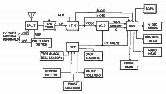
Fig. 10-14. Block diagram of KR9000 units record mode.
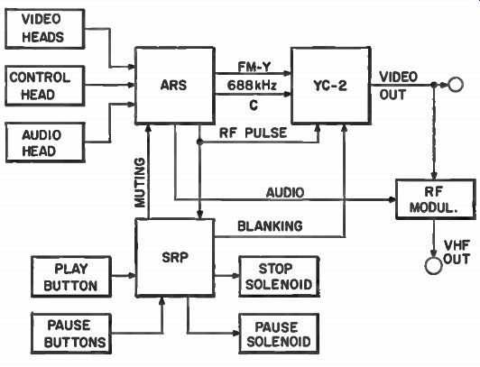
Fig. 10-15. Block diagram of KR9000 units playback mode.
Luminance (Video) Playback System
Refer to the block diagram in Fig. 10-16 as we review this video playback system. As the video heads rotate during the playback mode they pickup the recorded information from the video tracks on the video tape.
The combined frequency modulated (Y) signal and 688 kHz chroma signals are coupled through the rotating transformer to the ARS board. There is a "chain" of three functional blocks for the output signal of each of the two video heads. The blocks, mostly inside IC2001, are: the pre-amplifier, the equalizer amplifier, and the switcher circuits. Input to this chain of blocks enter the IC at pins 23 and 24. A 30 Hz signal, the RF switching pulse, at pin 18 switches the processed signals to pins 16 and 17, in time with the active tracking of each head. There are three possible signal outputs from the three center-tapped resistances across pins 16 and 17: monochrome, the luminance portion of the color program, and the chroma (at 688 kHz). Test Point 5 is the take-off point for a black and white signal to pin 14 of IC2001 and internally to the B/W position of a switch.
The other switch position is marked "color" and is connected to pin 15. A signal containing both color and B&W can be taken off the top pair of resistors and through the HPF block to pin 15. Only the Y -FM luminance information is connected through the high pass filter (HPF), because the Y -FM signals are in a high range of frequency by comparison to the chroma frequency. Therefore, no color information goes through to pin 15. Thus the signal that is to be processed further in IC2001 is strictly luminance.
The condition of the internal switch connected to pins 14 and 15 is determined by the DC voltage on pin 12. This voltage is the playback automatic color killer (PB ACK) signal. If there is no color information in the playback video tape the pin 12 voltage is 0 and the internal switch is in the B/W position. Thus the monochrome signal is coupled from pin 14 through to the Limiter block. If there is color in the video signal the pin 12 voltage is about +4 volts and the internal switch is in the color position and the pin 15 signal is coupled through to the limiter block.
In either case the Luminance signal continues through the drop out compensator block and out pin 4 to Q2007, a buffer stage. The buffer output goes in two directions. One is up and to the left through DL2001, a delay line that delays the signal for a period of one horizontal line, about 63 microseconds. The delayed, fed-back signal is coupled to the drop out compensator by way of pin 6.
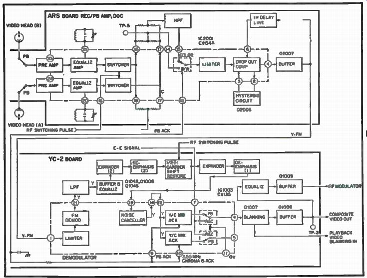
Fig. 10-16. Luminance playback system.
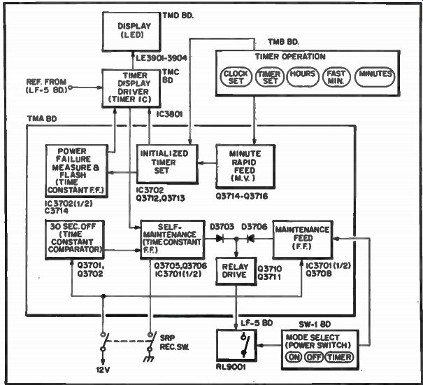
Fig. 10-17. Clock timer block diagram for KR9000 VCR.
The purpose of the drop out compensator is to insert the 1H (1 horizontal line) of delayed picture information into the main signal in place of dropout, or no information, on a horizontal line during playback.
The Y-FM signal moves out of the ARS board and into the YC-2 board and pin 1 of IC1003. Inside the IC the signal is limited to eliminate amplitude variations before it is coupled into the FM demodulator. The demodulator output, which is the original Y -FM signal as well as the recovered lower frequency luminance signal, appears at pin 21.
A low pass filter (LPF) selects only the demodulated low frequency luminance and couples it through to a buffer and equalizer block and then upward and on to the right through a chain of functional blocks.
These blocks include expanders and de-emphasis circuits. The emphasis added to the high luminance frequencies for the record mode now must be counteracted, otherwise the high frequencies of the playback signal will be distorted, of higher amplitude than the original transmitted TV signal.
The de-emphasized signal returns to IC1003 at pin 19 and inside to the noise canceller block. Out pin 14 and back in pin 12 goes the signal and then into two similar blocks, labeled Y/C mixers. Within these blocks the mixing of the playback luminance and chroma signals takes place and the outputs are connected to the PB (playback) positions of the internal switches coupled to pins 4 and 5. In the playback mode of operation the pin 11 voltage is 0 volts, and the switches are in the PB positions. The playback luminance signal couples out of pin 4, past the blanking block and through the Q1008 buffer, to the video out jack and through to the RF modulator.
The blanking transistor, Q1007, is in shunt with the signal path between pin 4 of IC1003 and the buffer stage. During normal operation Q1007 is not conducting and is a high impedance to ground and does not affect the video signal flow. Usually when the VCR is first turned on in the play mode, the tape movement is not up to normal speed. Then the SRP board couples a positive voltage to the base of Q1007, turning it on to saturation. The result is a very low impedance to ground for the output luminance signal, which is thus routed to the ground. Without a video signal into the TV receiver the picture tube is blanked out. When the correct tape speed is reached, the blanking stage is cut off and a normal picture appears on the TV receiver screen.
Clock Timer
A block diagram of the complete clock timer for the Zenith VCR recorder is shown in Fig. 10-17.