In this Section we will look at electronic digital clocks that are used with clock radios. Circuit operation and some troubleshooting tips will be covered.
ELECTRONIC DIGITAL CLOCK CHECKS (ZENITH MODEL 1480)
The following check should be made to verify proper operation of the electronic digital clock.
In the normal mode of operation, the clock will display real time in a 12-hour format. Move the clock time switch to "time set". Depress the fast button. Time should advance at 60Hz rate. AM and PM indicators, to the left of the time display, should change state when time passes through 12:00. Depress the "slow" button. Time should advance at about a 1 Hz rate. Move the clock time switch to "alarm set". This should cause the display to switch from real time to alarm time. While in "alarm set" position, depress "fast", then "slow" Buttons. Alarm time should advance as previously described for real time settings.
Move clock time switch to "run". Depress the "sleep switch". Radio should turn on and display should switch from real time to sleep time.
Starting at 59, display should count down at about 1 Hz rate until the button is released. When released, display should revert to real time but radio should continue to play until internal counter counts down to zero at a one minute rate.
Touch the. "Touch 'n' Snooze" plate. The radio should turn off.
Depress "sleep switch". Radio should turn on and the display show the number of sleep time minutes remaining. Continue depressing the "sleep switch" until counter reaches zero. Radio should turn off.
Set the function switch to "auto radio". The alarm check indicator should illuminate. Move clock time switch to "alarm set" and note time of alarm setting. Move clock time switch to "time set". Using the "fast", then "slow" buttons, advance real time up to alarm time. Radio should turn on at precise alarm time setting.
Touch the "Touch 'n' Snooze" plate. Radio should shut off for about nine minutes. Check by advancing real time with "slow" button. This cycle should be repeatable for about one hour from the alarm time setting.
Repeat the two steps above with the Function Switch in "auto alarm" position.
Temporarily disconnect the line cord from the AC socket. When the line cord is re-connected, the display digits and AM/PM indicator should be flashing on and off. Depress "fast" or "slow" buttons (in "time set" position) or depress "sleep switch". Flashing condition should stop. To verify proper operation of the power fail circuit make the operational check.
Troubleshooting the Digital Clock A block diagram of the clock circuit is shown in Fig. 9-1. Input and output connections to the clock IC are shown as well as interconnections between the IC and clock display. The IC chip connections shown in Table 9-1 will also help you when troubleshooting this clock circuit.
MOS Circuit Care
The following precautions should be taken so as not to damage the MOS IC in this clock system.
• Always turn off the power to unit before replacing the MOS IC chip.
• Avoid electrostatic build-up which can occur by contact with wool or synthetic materials.
• Working surfaces, test equipment, and soldering irons must be at the same reference (ground) potential as the devices under test and the container for the devices.
Display Dimmer Circuit
A built-in light sensor will automatically adjust the clock display intensity, based on changes in room lighting. A light dependent cadmium sulfide cell (R901), mounted to the lower left of the clock display, functions as a light sensing element. This cell, in parallel with R726, is connected from +24.4 volts output of the bridge rectifier to the base bias circuit of the auto dimmer transistor Q708. Q708 is connected between the low side of the clock displays common cathodes and ground. Light variations will effectively vary the Q708 base circuit resistance, changing base bias, resulting in a corresponding change of current flowing through the clock display segments and hence the intensity of the segments.
Power Failure Protection Circuit
During normal operation, with AC power applied to the radio set, transistor Q503 is conducting, transistors Q504 and Q505 are off, and multivibrator Q501, Q502 is "locked-up".
When power to the radio set is interrupted, the DC voltage at point "HH" begins to drop from a nominal 24.2 volts toward 0 volts. When the reading reaches about 10 volts, the voltage drop across voltage divider R507/R509 biases transistor Q503 off. This in turn biases on transistor Q505 which allows capacitor C505 to charge and enable DC to DC converter Q504/T501 to oscillate. Output of the converter (about 20 kHz) is rectified and filtered by CR503 and C514 respectively.
The resultant DC voltage is maintained and regulated at about 10 volts by Q503. This voltage is used to enable multivibrator Q501/Q502.
The multivibrator is designed to produce a modified 60 Hz square wave output at point "II" which is used to maintain the operation of the clock IC. The power failure protection circuit will continue to operate as long as sufficient battery voltage is available to allow capacitor C505 to charge through Q505 (normally four hours with a fully charged battery at time of power interruption). When power is restored, the NI-CAD battery begins charging. Note that during a power interruption, the voltage normally at the output of full-wave rectifiers CR501, CR505 is not present, therefore, display CR701 is not illuminated.
A simple check with the oscilloscope can be made to verify proper operation of the power failure protection circuit.
If Ni-CAD battery is in a completely discharged state, connect radio to AC power line for at least 15 minutes to obtain a partial charge on the battery. Attach ground lead of scope to chassis ground and probe scope to point "H" on power fail circuit board (60 Hz output pin). For normal operation the scope will display a half-wave rectified sinewave as shown in Fig. 9-2.
Disconnect the AC line cord. The wave shape should change within one or two seconds to the waveform shown in Fig. 9-3.
This waveform will disappear in a few seconds if the battery is not fully charged. If, however, the waveform will disappear completely as soon as the AC line cord is disconnected, the power fail circuit is inoperative and must be repaired.
With the AC line cord connected, set real time to approximately five minutes before alarm time. Move radio function switch to "auto alarm". Disconnect AC line cord. Tone alarm should sound in approximately five minutes. This confirms that the tone alarm circuit will function in event of a power failure.
Repeat the same procedure as above, except that the radio function switch should be in the "radio alarm" mode. When alarm time is reached, only the tone alarm will be heard. The radio will not be heard and clock display will be blank.
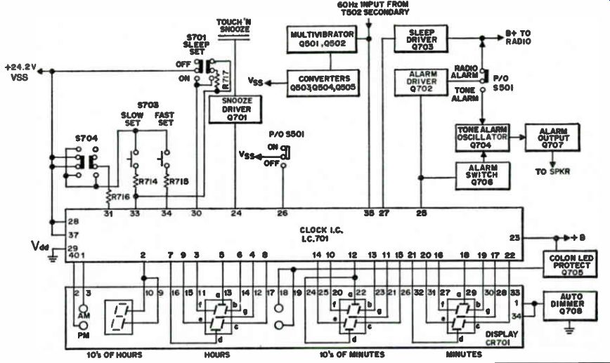
Fig. 9-1. Simplified digital clock readout circuit.
---------------- Table 9-1.Clock IC701.
PIN NO. CONNECTION REMARKS
1 AM OUTPUT 2 10's of HOURS b&o 3 HOURS f 4 HOURS g HOURS a 6 HOURS b 7 HOURS d 8 HOURS c 9 HOURS e 10 10's of MINUTES f 11 10's of MINUTES g 12 10's of MINUTES a&d 13 10's of MINUTES b 14 10's of MINUTES e 15 10's of MINUTES c 16 17 18 19 20 21 22 MINUTES f MINUTES g MINUTES a MINUTES b MINUTES e MINUTES d MINUTES c
Drives segment f of 10's of hours digit. Approx. +15.7 VDC when AM LED is ON. OV when OFF Both segments either ON or OFF simultaneously. Approx. +15.7V when ON. OV when OFF. Pins 3 thru 9 drive HOURS 7-segment LED. Approx. +15.7V when given segment is ON, OV when OFF. Pins 10 thru 15 drive 10's of MINUTES 7-segment LED. Approx. +15.7V when given segment is ON. OV when off.
Pins 16 thru 22 drive MINUTES 7-segment LED. Approx. +15.7V when given segment is ON, OV when OFF. 23 OUTPUT COMMON SOURCE Approx. 17 VDC. Insures low output ON resistance to DISPLAY. 24 SNOOZE INPUT Momentary application of Vss to pin 24 inhibits alarm output approx. 9 minutes.
25 ALARM OUTPUT +24.2V when activated. Enables alarm output driver for 59 minutes or until temporarily inhibited by Snooze Alarm Input (pin 241 or reset by Alarm OFF Input (pin 261.
26 ALARM OFF INPUT Momentary application of Vss to pin 26 resets alarm latch.
27 SLEEP OUTPUT +24.2 VDC when activated. Biases on Sleep Driver for up to 59 minutes.
28 Vss 29 Vdd 30 SLEEP DISPLAY INPUT t . 31 ALARM DISPLAY INPUT 32 SECOND DISPLAY INPUT 33 SLOW SET INPUT 34 FAST SET INPUT 35 50/60 Hz INPUT 36 60/60 Hz SELECT 37 BLANKING INPUT 38 12/24 HR. SELECT 39 1 Hz OUTPUT 40 PM OUTPUT +24.2 VDC (Clock 6+). OV (Chassis ground). Display Mode Select Inputs. Programs selected display when Vss is applied to pin. In absence of inputs, real time is displayed.
Not used.
Time Setting Inputs. Application of Vss to these inputs advances clock time.
60 Hz modified sine-wave. 20 to 25 V pp.
Not used for 60 Hz operation.
+24.2 VDC. Application of Vss to pin 37 enables display. Vdd inhibits display.
Not used for 12 Hour format.
Not used.
Drives segment e of 10's of HOURS digit. Approx. +15.7V when ON, OV when OFF.
----------------
Clock IC Function Chart
To make troubleshooting easier refer to the clock IC function chart (Table 9-1) which gives IC 701 pin outs and their functions.
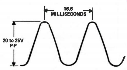
Fig. 9-2. Correct 60 Hz waveform.
---------------
Fig. 9-3. Correct waveform change after radio is unplugged for two seconds.
NOTE: This waveform will disappear in a few seconds if battery is not fully charged. If, however, the wave form disappears completely as soon as AC line cord is disconnected, the power fail circuit is inoperative and must be repaired.
-------------- FM Multiplex Decoder (Used in Zenith Digital Clock Radio)
A phase locked loop (PLL) oscillator circuit eliminates the need to regenerate the 38 khz subcarrier. Therefore, phase accuracy of the 38 kHz signal is only limited by the loop gain of the system and by the stability of the oscillator frequency. Both of these parameters can easily be control led, providing fast, easy adjustment and long term stability.
Basic functions of IC 301 are as follows. Note block diagram of the decoder in Fig. 9-4.
Regeneration of the 38 kHz subcarrier frequency.
Stereo indicator switching.
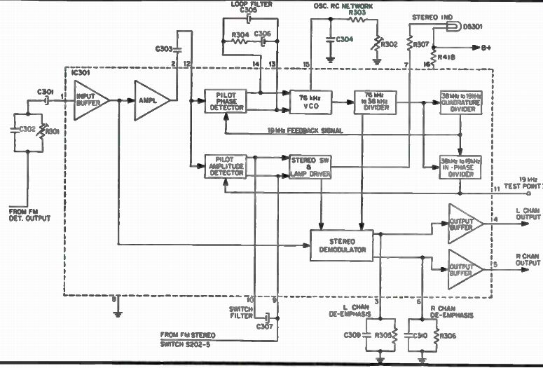
Fig. 9-4. Block diagram of FM multiplex decoder.
Decoding the multiplex signal (matrixing the L + R and L-R, 38 kHz)
to provide the L and R outputs.
The phase locked loop is comprised of the following.
Pilot phase detector.
76 kHz VCO. 76 kHz to 38 kHz divider.
38 kHz to 19 kHz Quadrature Divider.
These circuits are used to regenerate the 38 kHz suppressed carrier required to demodulate the multiplex signal.
A multiplex signal from the FM detector is fed through pin 1 to the input Buffer which provides a high impedance input and unity gain to the demodulator. The amplifier which follows the buffer, provides a gain of three to the pilot phase detector and amplifier detector.
Pilot phase and amplitude detectors are synchronous, balanced chopper types which develop differential output signals across external filters. Chopper transistors in the phase detector are driven from the quadrature divider. The 19 kHz pilot signal from the Quadrature detector is compared with the 19 kHz pilot signal contained in the multiplex input signal. Error signal developed across the loop filter controls the 76 kHz VCO. In the phase locked condition, the pilot signal is in quadrature with the internal 19 kHz signal.
A 76 kHz RC relaxation type (VCO) generates a positive low duty cycle 76 kHz output, whose free-running frequency is controlled by external components. This VCO also uses the differential error voltage from the pilot phase detector for phase lock to the 19 kHz pilot.
A 76 kHz to 38 kHz divider converts the 76 kHz from the VCO into a 38 kHz square wave in a simple divide-by-two circuit. The 38 kHz square wave output is fed to the stereo demodulator, 38 kHz to 19 kHz quadrature divider and also the 38 kHz to 19 kHz in-phase divider. The 38 kHz to 19 kHz in-phase divider develops a 19 kHz signal which is in-phase with the pilot signal. The in-phase divider is controlled by both the 76 kHz to 38 kHz divider and the 38 kHz to 19 kHz quadrature driver to prevent 180 degree phase ambiguity. Its output drives the pilot amplitude detector which is the same as the pilot phase detector, but because of the in-phase relationship of the 19 kHz drive with the pilot, this detector operates as a synchronous amplitude detector instead of a phase detector. A 19 kHz test signal is provided through pin 11 to test point "I". The differential voltage developed across the switch filter C307 drives the stereo switch and lamp driver.
Stereo indicator lamp is driven by the stereo switch and lamp driver which also enables the stereo demodulator, when a stereo signal is present.
The stereo demodulator is a fully balanced synchronous detector type which receives the multiplex signal from the input buffer, the regenerated 38 kHz subcarrier from the 76 kHz to 38 kHz divider and the stereo/mono switching voltage from the stereo switch and lamp driver. Left and right output signals are developed across external resistors to ground from pins 3 and 6.
Squelch Circuit (Transistor Type)
This squelch circuit is used in various AM/FM/Aircraft and public service radio receivers.
The basic squelch circuit (see Fig. 9-5), uses two directed coupled transistors (Q401, Q402). The bias voltage of the first squelch transistor (Q401)is determined by the position of the squelch control (R402) which is part of a voltage divider network connected between B+ and B-. When the control is a minimum (near B+) Q401 is turned "on". Q401 collector current through R407 will turn Q402 "off". As control R402 is advanced (toward B-) a point will be reached (under no signal conditions) when forward bias on Q401 has been reduced to a point of "cut off". When this occurs, Q402, will be turned "on". Q402 collector voltage will appear at diode CR401, turning the diode "on", applying bias to Q403, reducing forward bias on Q403, thereby turning the audio off.
When a signal appears at the Q206 collector, it is coupled via capacitor C238 to a diode doubler circuit, (CR206, CR207). One end of the doubler is connected to B- while the other end is connected Q401 via resistor R405. When the voltage of the doubler circuit is of sufficient amplitude, it will overcome the preset squelch voltage on Q401, causing Q401 to turn "on", turning Q402 "off' and allowing Q403 to conduct, thereby passing audio on to the sound output stages.
Service Notes
The most common troubles in this circuit will be defective transistors, diodes and resistors that have changed value.
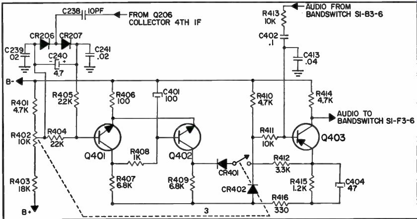
Fig. 9-5. Transistor squelch circuit.
RCA TV DIGITAL CLOCK AND SCREEN READOUT SYSTEM
The following digital/clock and TV screen readout circuits are found in some of the late model RCA remote control color TV receivers.
Clock and Display System
The clock and display circuitry provides two basic functions for the digital address system.
Converts the channel number BCD code generated by the control IC to video signals, which allow the channel number to be displayed as decimal characters on the TV screen.
Generates and maintains time-of-day information in an hour and minutes digital format, which is also converted to video signals to be displayed on the TV screen simultaneous with the channel number.
The clock and digital system also, in response to time out, half-entry, and CTS codes from the control IC, sets the color of the display (white, red, or green) and the amount of time the display remains on the screen.
A block diagram of the basic clock and display system is shown in (Fig. 9-6). The channel number BCD code is coupled from the control IC on the command module to the clock IC located on the clock and display module.
The clock IC also receives 60 Hz clock pulses from the crystal controlled reference clock located on the command module. The clock IC converts both the BCD code and the clock information to a channel number and time-of-day display code for use by the display IC. The time-of-day may be updated by the viewer via hours and minutes update push buttons located on the front control panel.
The display IC decodes the display code from the clock IC and the CTS code from the control IC to provide the proper series of color blanking and luminance drive pulses to the sets video circuitry for character display on the TV screen. Auxiliary blanking is provided to both the luminance and chrominance circuitry to blank station video and color outputs during character display. Horizontal and vertical sync is also defeated during half-entry and non-assigned channel entry to prevent noise from causing character display instability.
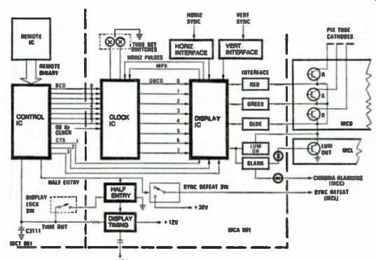
Fig. 9-6. Direct address display system.
The amount of time characters in white are displayed on the screen in governed by display timing circuitry also located on the clock and display module. The viewer can, however, "override" this circuitry and cause the display to remain on the screen continuously by activating the "display lock" switch located on back of the set.
The BCD code and reference clock information applied to the clock IC is converted to a display code. This code consists of two, four-bit words, that are converted to corresponding character video signals in the display IC as illustrated in (Fig. 9-7). The timing of the display code appearing on the clock IC DBCD outputs is governed by "multiplex" pulses generated in the display IC an horizontal sync pulses from the chassis deflection circuitry. The multiplex pulses apply the display code alternately to each set of DBCD outputs (0-3, 4-7). However, the code actually appears on the proper outputs one multiplex pulse before it is "read" by the display IC. In this manner, optimum character stability is achieved as one set of outputs is "settling down" while the other is being read.
The multiplex pulses are derived from a 2.5 MHz reference pulse train divided from a 5 MHz oscillator located in the display IC. The 2.5 MHz reference pulse also provides the timing for the video blanking pulses which represent each character. Figure 9-8 illustrates the relationship between the character format, the 2.5 MHz reference pulses, and the output blanking (video) pulses. The horizontal sync pulses set vertical alignment of the characters from one horizontal line to the next by synchronizing the first multiplex pulse to horizontal retrace and thus initiating the order of the DBCD readout.
Note in Fig. 9-8 that each character occupies a rectangle 20 vertical lines high (interlaced to 40) and 8 reference pulse periods wide. Character generation starts on the 192nd horizontal line after vertical sync and ends on the 212th horizontal line. The 5 MHz reference oscillator in the display IC is synchronized with horizontal sync pulses coupled from the chassis deflection circuitry through input interfacing stages. Applied vertical sync pulses provide a reference for establishing character vertical positioning.
The display output interfacing circuitry consists of emitter followers in the red, green, and blue blanking outputs, as well as the luminance and chrominance blanking outputs. The luminance drive is a transistor switch and resistor stage designed to provide the correct driver output current for proper saturated (white or color) characters. Figure 9-4 illustrates in simplified form the inter-relationship between the display interfacing and the sets video circuitry. For explanation purposes, the display waveforms generated are those for the character "1" as shown in (Fig. 9-10). For this digit, the pulse shape applied to the red, green, and blue (Q7-9) interfacing emitter followers is as shown in (Fig. 9-9). Note that blanking is applied to the leading and trailing edges of the character. During these blanking intervals, current is diverted from the red, green, and blue output stages, causing a black area to surround the digit. This greatly enhances the sharpness and visibility of the character.
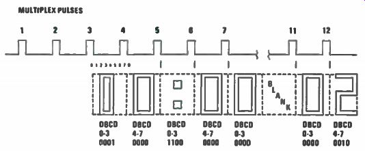
Fig. 9-7. Clock IC outputs.
A luminance drive pulse is supplied to transistor Q5 which establishes the video output driving current for proper white saturation. If blanking were applied for the full character width to any combination of the R, G, B blanking stages, along with luminance drive, the character would be produced in full color. This is illustrated by the "0" in (Fig. 9-8). Of course, blanking applied to all three color stages simultaneously would completely blank the video, producing a black screen (muted video). This occurs during half entry or wrong channel input, except in those areas where the characters are displayed.
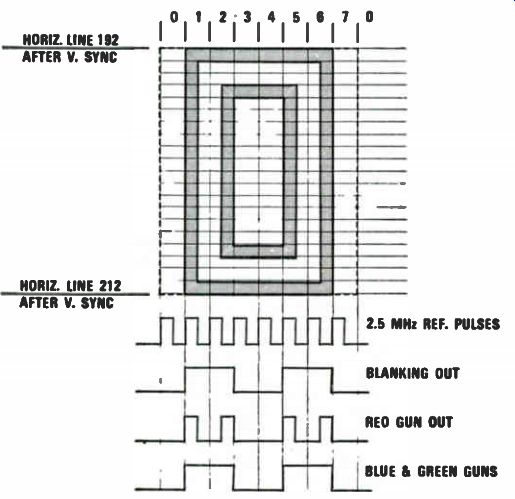
Fig. 9 - 8. Display format of red "0" with output waveform.
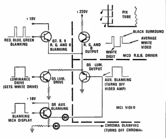
Fig. 9-9. Display - Video Drive for Digit No. 1.
An auxiliary blanking pulse (which is the same as the luminance drive pulse) is applied to an auxiliary blanking emitter follower Q6. This stage cuts off the luminance output stage (Q5 on the video module), preventing station video information from appearing on the screen during character display and provides a blanking pulse to IC2 on the chroma module which prevents station chroma input to the R, G, and B outputs.
Referring again to (Fig. 9-6), note that the half-entry terminal is coupled to an electronic sync defeat "switch". This switch provides a positive voltage to the base of the PNP sync separator (Q3), disabling this stage during half-entry and wrong channel selection. This defeat is necessary to limit vertical instability of the character display when no valid station sync information is received.
Figure 9-11 illustrates the display timing circuitry. A character display will appear in white on the screen whenever the time-out terminal on the control IC is taken low (toward ground). This automatically occurs when any command (except volume up or down) is received. The display will "time-out" (disappear) when the time-out becomes sufficiently positive. This is caused to happen by allowing capacitor C3111 (located on the command module) to charge from +12 volt DC supply through transistors Q10 and Q11. These transistors are normally biased into saturation making the charging time constant dependent on R43 (270K) and the value of C3111, of about 4 seconds.
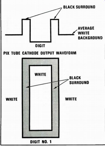
Fig. 9-10. Comparison of white 1 digit to output waveform.
PIX TUBE CATHODE OUTPUT WAVEFORM
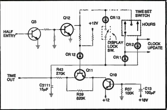
Fig. 9-11. Display timing circuitry.
During half-entry, it is desired to extend the display "time-out" to give the customer sufficient time to enter the second digit before the safety-time-out feature turns off the receiver. This extra half-entry time is provided by turning off Q11 through elimination of forward bias supplied by the half-entry "switch", Q3 and Q12. During half-entry, Q3 turns on, turning off Q12, which removes Q11 forward bias. The C3111 charging time constant then is extended to approximately 15 to 20 seconds by the addition of resistance R39. The half-entry switch also disables the display-lock switch and the time-set switch operation during half-entry, by removing the ground return through Q12.
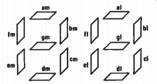
Fig. 9-12. LED display and logic conditions.
When power is initially applied to the chassis, it is desired to have the display visible when the picture tube warms up. This is accomplished by delaying the turn on of Q10 for approximately 10 seconds by charging capacitor C13 from the 18 volt power supply bus, which is derived from the chassis 38 volt power supply. The voltage on the base of Q10 will decay toward the turn-on voltage of this device as C13 discharges through R37.
TV Channel Indicator LED Display
The LED display decoder driver IC is used to drive a two-digit, seven-segment LED channel indicator. Eight lines of binary coded decimal (BCD) information is supplied to the IC located on the control module to allow continuous, non-multiplex operation. The code which relates to the input and output states is the standard BCD-to-seven segment code which activates the appropriate segment(s). The LED display chart, (Fig. 9-12), gives the logic condition or output code of the LED Display Driver IC. If a problem occurs resulting in loss of, or incorrect LED display, the chart will aid you in determining if the problem exists in the MSC module or LED assembly.