High Voltage Protection Circuit
The circuit as shown in Fig. 32 looks like the horizontal "hold down" circuit in other XL-100 chassis. However, it should be noted that the circuit as used in the CTC 74, and CTC 81 chassis is not used to meet (HEW) requirements.
The circuit comprised of Q501 (and associated components) is designed to disable the horizontal sync circuits in case an open develops in the horizontal trace ITR circuit. The oscillator is forced off frequency, in the direction that prevents damage to components in the deflection circuit.
Under normal operating conditions (and most "failure" conditions) the circuit of Q501 is not conducting; cut-off state is maintained due to the reverse bias of the base-emitter junction-set by the 6.8-volt Zener diode in the emitter. Quiescent "positive" voltage, developed vi -a CR504 from the sweep pulse (negative going), is not sufficient to overcome the base-emitter junction. Under these conditions, the horizontal hold circuit (located in the MCH module) is unaffected, receiving its normal operating potential - the horizontal will remain in sync.
Note that the pulse available to the anode of CR504 (from terminal 13) is highly negative; in other chassis where this circuit acts as a hold-down - a "positive" pulse is applied at a comparable point, as a sampling of the high voltage being developed. Here, an unusual failure must occur in the deflection system, to cause a signal with "positive-going" excursions at the anode of CR504 - sufficient to be rectified, fed to the resistive network of R516, R517 and the base of Q501 ++ turning the transistor on. With this transistor biased into conduction, the DC potential applied to the horizontal hold control (about 30 volts under normal conditions) is clamped to about 6.8 volts (CR506 in the emitter circuit). This voltage change drives the horizontal oscillator well off frequency, causing a loss of horizontal sync, protecting the deflection circuit until the fault is located and repaired.
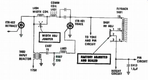
Fig. 31. Simplified horizontal deflection circuit.
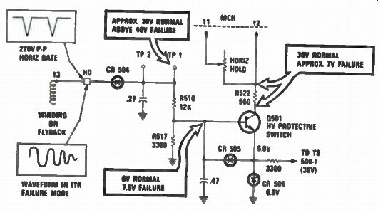
Fig. 32. High Voltage protection circuit - RCA CTC 74.
Because its purpose is different, troubleshooting and testing the "protective" circuit in the CTC74 or CTC81 chassis requires a different procedure than used for the "hold-down" circuit in other XL-100 chassis.
You may recall, the circuit of Q501 is normally at cutoff, having no effect on the horizontal oscillator. A negative going pulse is normally fed to the anode of CR 504 and, a pulse with high, positive going excursions - such as caused by an "open" failure in the trace ITR circuit - must be present at CR 504 to switch Q501 to an "on" mode.
Trace/Retrace Service Information
Possible damage to deflection components could occur if the trace ITR (or circuit) is defective. The protective stage is then defeated, and power is applied. Of course, a fault could develop within the Q501 stage, causing loss of horizontal sync; however, the original cause (or circuit) can be located by a proper sequence of servicing checks.
Assuming a loss of horizontal sync, the following service procedures should be used:
• Replace the MCH module with a good module, and readjust the customers hold control. If sync is restored at about the center of control range, a defective module is indicated.
• If, with adjustment of the customer's control, the oscillator can be adjusted close to sync, center the hold control and slightly adjust the horizontal range control on the MCH module to sync-in the picture.
• If conditions do not improve, measure the DC voltage at terminal 12 of the MCH module. If other than normal voltage is present at this point, replace the trace ITR, and recheck for correct operation, indicated by the return of sync, and/or a proper voltage at terminal 12.
• An abnormal voltage (6.8 volts) at terminal 12 of the MCH module confirms the "protective circuit" is "on", but does not indicate whether the origin is a defect, or caused by a component failure associated with the protective circuit (an emitter-to-collector short, for example). A DC voltage check at TP 1, TP 2, or the base element will indicate if the stage is being keyed on; viewing the waveform at point HD will yield the same result.
• A normal voltage at terminal 12 of the MCH module, indicates the protective circuit is not causing a loss of sync. The strong possibility now exists of problems in circuits associated with, or operating in conjunction with, the horizontal oscillator.
After any servicing operations, the protective circuit should be checked for proper operation. The value of some components, and the normal operating voltages in the CTC 81 circuit are slightly different than in the CTC 74 circuit. The circuit as used in the CTC 74 appears in Fig. 32, while the CTC 81 circuit is shown in Fig. 33.
Operation in the CTC 74 can be checked out as follows: Set the line voltage to 120 volts AC and all controls for a normal picture. Momentarily short across R516 with a 12 K resistor. Under these conditions, the picture should lose horizontal sync, and the raster will become dimmer than normal. If these symptoms occur, the protective circuit is capable of working properly.
Operational checks in the CTC 81 follows the same basic procedure, however, R516 in the CTC 81 chassis is 18K, requiring another value resistor to come up with a resistance of 6K. A resistor substitution box can be used to shunt across R516. Loss of the horizontal sync should now occur under the above conditions. Voltages and waveforms during normal and abnormal operation should approximate those that are indicated in Figs. 29 to 31. The ringing, sine-shaped waveform (see Fig. 32) at point HD is representative of the signal with an "open" in the trace circuit.
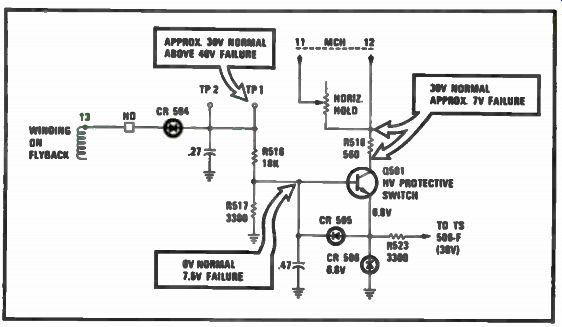
Fig. 33. High Voltage protection circuit - RCA CTC 81.
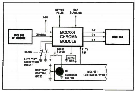
Fig. 34. Chroma module and related systems.
CHROMA SYSTEM (RCA SOUD/STATE IC'S)
The following IC circuits are used in the RCA CTC74 and CTC81 color TV chassis.
Chroma information is coupled from the MCK 001 IF module to the MCC 001 chroma module (See Fig. 34) which amplifies and demodulates the chroma sidebands, providing color difference signals to the driver module MCD 001. The chroma module is supported by several external circuits such as the color and tint controls.
Some other inputs to the MCC 001 chroma module are horizontal rate keying pulses and blanking voltages for sets with digital address options.
Built within the chroma module is a regulated DC supply fed from the chassis 28 volt source and referenced to an 11.7 volt regulated supply derived in the luminance/sync module.
Chrome Module Circuits (MCC 001)
Looking at Fig. 35, note the chroma sideband information of about 600 mV enters the chroma processor integrated circuit, ICI. This circuit performs a number of functions including chroma amplification, automatic chroma control (ACC) and color subcarrier regeneration and control (AFPC). The exact frequency of the 3.58 MHz color subcarrier is set by crystal Y1 and capacitor C11. The color reference signal (burst) is separated by an internal gate activated by the 1 volt keying pulse that is fed to pin 9 of IC 1.
The processed chroma exits IC 1 via pin 15 and is capacitively coupled to pin 3 of the chroma demodulator, IC 2. The 3.58 MHz CW subcarrier information enters IC 2 on pin 16 at the proper phase to provide "I axis" chroma sideband demodulation. A phase shift network, consisting of R12, Li, C28 and C25 sets a 90 degree phase shift for the subcarrier to allow for "Q axis" demodulation. A customer color control, R4203 sets the gain of the IC 2 input chroma amplifier.
The subcarrier information may be phase shifted by an internal tint control circuit. The degree of phase shift is adjusted by the tint control pot, R4204. The demodulation process yields R -Y, G-Y, and B-Y difference signals at the proper respective amplitudes.
The regulator transistor, Q1, provides an 11.7 volt DC regulated supply for operation of the chroma module. Power is supplied from the chassis 28 volt DC source, but the regulator is referenced to the 11.7 volts in the MCL 001 module. This reference is used in order to maintain luminance to chroma tracking with contrast settings independent of supply voltage changes.
The Chroma Processor (IC 1)
A simplified block diagram of the chroma processor (IC 1) is shown in Fig. 36. Chroma sideband information entering pin 1 goes to a linear chroma amplifier which is gain controlled by an automatic chroma control voltage developed in the ACC detector. The amplified sideband information is then coupled to the AFPC and ACC detectors as well as the second chroma amplifiers.
The AFPC detector has the reference subcarrier (burst) gate and phase detector for phase locking the 3.58 MHz subcarrier oscillator.
Capacitor C16 is an external filter for the AFPC circuitry while C11 and Y1 set the operating frequency for the oscillator.
The ACC detector is gated to allow burst input from the first chroma amplifier. Also applied is a phase shifted input from the 3.58 CW oscillator.
This phase shift allows the ACC detector to become sensitive to amplitude variations in burst levels. These variations are filtered by capacitor C5 and fed back to the first chroma amplifier, providing gain control for this stage.
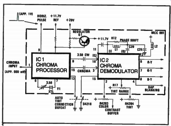
Fig. 35. Simplified chroma module diagram.
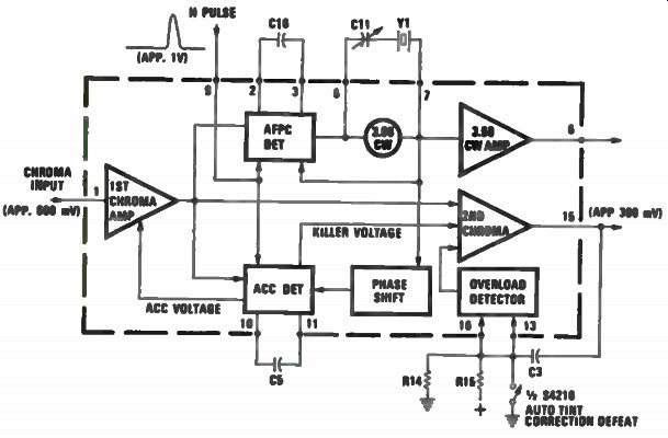
Fig. 36. Block diagram of chroma processor module.
Loss of a burst signal causes the ACC detector to produce a voltage which cuts off the second chroma amplifier. Thus, the chroma circuitry is effectively "killed" when black and white picture information is received.
The IC also has an overload detector which reduces the gain of the second chroma stage upon reception of an abnormally high saturated chroma signal.
The Chroma Demodulator (IC 2)
In Fig. 37 we see the chroma demodulator, IC 2. The chroma sidebands at about a 300 mV level are first applied to a gain controlled chroma amplifier. The gain of this amplifier is determined by adjustment of color control, R4203. Chroma blanking for digital address display (DAP) is also applied to this stage of the circuit. From the amplifier, the chroma sidebands are coupled to the "I" and "Q" demodulators.
The 3.58 MHz CW subcarrier enters IC 2 on pin 16 at a level of around 400 mV. The nominal phase of the subcarrier after being fed to the IC allows demodulation on the "I axis". However, the subcarrier phase can be altered by a DC controlled phase shifting (tint control) circuit. Control of this circuit is by the tint control, R4204, and a "tint range" centering control. Inductor L2 and its distributed capacity is broadly tuned to 3.58 MHz in order to restore a sinewave shape to the subcarrier waveform, which is distorted in the tint control circuit. The output of the tint control circuit is then fed to the "I" demodulator, via an adder stage, which has no effect on the subcarrier signal if the automatic tint correction feature is defeated.
A phase shifting network consisting of Li, C28, and C25 provides the 90 degree subcarrier phase shift for "Q" demodulation. The outputs of the "I" and "Q" demodulators are coupled to a matrix which provides the R -Y, B -Y, and G -Y difference signals at their proper amplitudes.
COMB FILTER CIRCUIT (RCA CTC 99/101 CHASSIS)
The purpose of comb filtering is to more perfectly separate the video signal and the chroma signal throughout the entire bandwidth of the video spectrum. Comb filtering greatly minimizes the crosstalk interference that would occur if chroma information were allowed to pass through the luminance channel. The comb filter operates on two basic principles.
• From one line to the next, the video information is basically the same. This means that as the picture is scanned vertically, there is very little change in the luminance information from one horizontal line to the next.
• Next, the chroma information on one line is 180 degrees from one line to the next, so the chroma information on one line is 180 degrees out of phase with the chroma information on the previous line.
Operation of the Comb Filter The heart of the comb filter is U601 (see Fig. 38), the comb filter integrated circuit chip. This IC contains the charge-coupled devices and provides all of the functions of comb filtering: the delay, the amplifiers for the video and chroma processing channels, and the summing circuits.
The U601 IC is powered from several power supplies. These are: 16 volts B+ pin 22, 9.1 volts B+ pin 9, -5 volts B- pins 1, 5, 6, and 7. Video information is coupled into U601 at pin 11. The 10.7 MHz clock pulse, developed from the 3.58 MHz chroma subcarrier frequency tripler circuit, is inserted at pin 3. Pin 21 is the combed luminance output. Pin 13 is the vertical detail information output and pin 14 is the combed chroma information output.
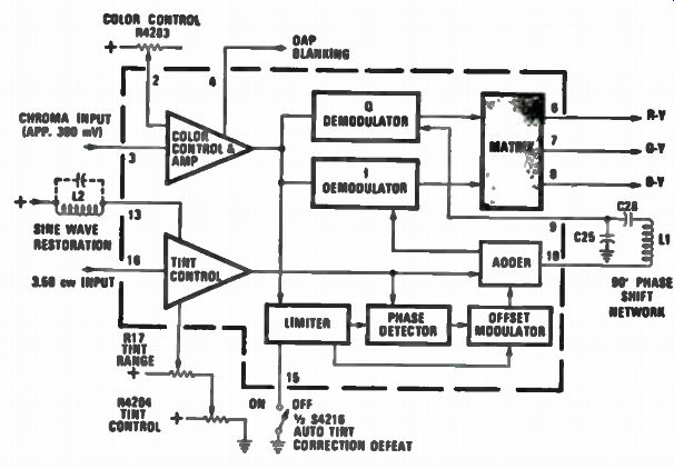
Fig. 37. Simplified block diagram of 1C2, on the chroma module.
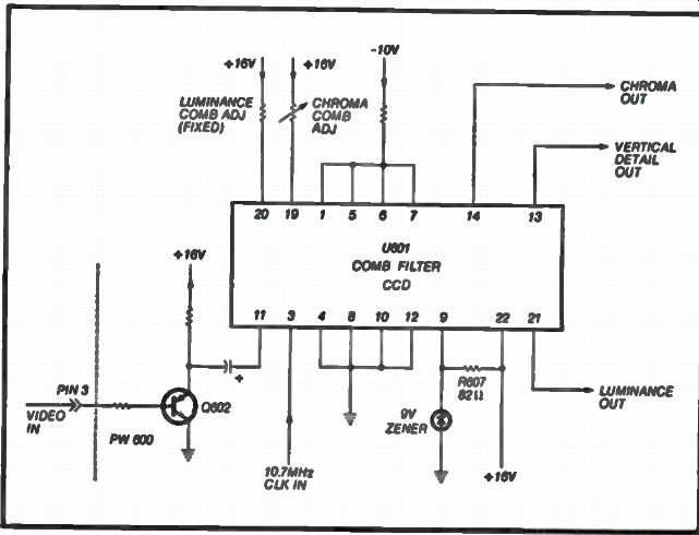
Fig. 38. Simplified comb filter diagram.
To understand the operation of the comb filtering, the frequency spectrum of the video signal in an NTSC frequency interleaved color system must be understood. The video signals occur between 0 and 4.2 MHz. However, to provide color transmission, a chroma subcarrier which is modulated by the color information is inserted at 3.58 MHz. The subcarrier, which is suppressed at the transmitter, creates sidebands which extend .5 MHz above the 1.5 MHz below 3.58 MHz.
To keep subcarrier sidebands from appearing in the luminance portion of the picture and generating crosstalk and other interference patterns, the video signal in a conventional receiver has a bandwidth of about 3 MHz. This minimizes the possibility of interference between low frequency chroma sidebands and high frequency luminance signals in the receiver's luminance channel. However, the limitations of video bandwidth causes a loss of high frequency (detail) picture information.
Note video spectrum in Fig. 39.
Comb filtering allows the recapturing of video information between 3 and 4.2 MHz, thus restoring a large amount of picture detail.
The relationship between the transmitted video information and the scanning rate causes the video information to occur in "bursts" of energy at the horizontal rate multiples. Therefore, at every 15.734 kHz from 0 to 4 MHz a "burst" of energy exists containing the video information. The chroma information also occurs in "bursts" of energy at the horizontal rate intervals. However, because of the selection of the chroma subcarrier frequency (3.58 MHz), the energy bursts are offset from the video energy bursts by one-half the horizontal rate. Thus, the chroma information is "interleaved" with video information.
Comb Filter Service Tips
Because the comb filter is just one of several circuits that process chroma and video information, the first step is to isolate the problem to the comb filter board or other circuitry, such as the IF, chroma processor, video processor, and etc. In Fig. 40 you will find the key scope input waveforms and other check points.
• Check for proper B+. Pin 9 of the PW600 board should read - 10 volts, and pin 11 should be +23 volts.
• Check for the presence of the video input signal at pin 3 of the PW600 board. If this signal is not present, the problem is in the IF circuitry.
• Check for the presence of the 3.58MHz CW at pin 7 of the PW600 board. This input is used to develop the delay line clocking pulses. Without this input, there will be no clocking pulses and the comb filter will deliver no output except noise. If the 3.58 MHz waveform is not at least 1 volt in amplitude, the comb filter will not be operational. If this voltage is incorrect, check the chroma circuitry for the defect.
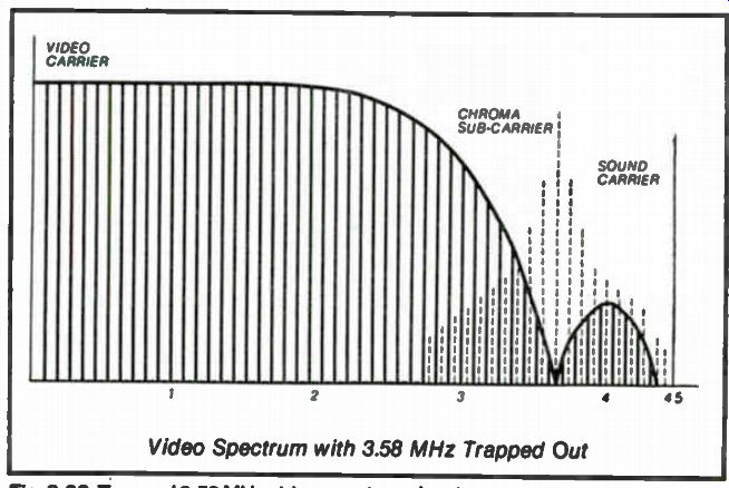
Fig. 39. Trapped 3.58 MHz video spectrum drawing.
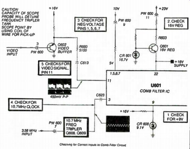
Fig. 40. Correct signal inputs of the comb filter.
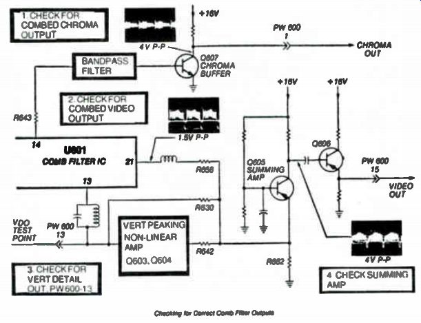
Fig. 41. Correct comb filter output signals.
• Check for chroma output signal at pin 1 of the PW600 board. If an output is present at this point, the problem is in the chroma circuitry.
• Check for video output at pin 15. If video output is present, the problem is in the video processing or video output circuitry.
• Check for the presence of the vertical detail output at pin 13. The lack of vertical detail output from the comb filter will appear as loss of picture resolution.
Loss of Video/Noise or Smearing in the Picture
Check the comb filter circuit U601 for +9 volts at pin 9 and for - 5 volts at pins 1, 5, 6, and 7.
Check pin 22 of U601 for the +16 volts regulated DC power. If this voltage is not present, suspect regulator transistor Q601 or Zener bias CR601 (16.7 volts) for the base of Q601.
Check at capacitor C623 for the 10.7 MHz clock signal. Do not connect the scope directly to the capacitor lead because the capacity of the scope probe on this circuit point will detune the frequency tripler. To check this signal, place a small loop of wire (or use scope pick-up loop) on scope probe tip and coil it around C623. This will feed enough signal to the scope without de-tuning the tank circuit. Because of the capacity coupling, it is impossible to specify a peak-to-peak voltage. However, if the signal is present, this indicates the tripler is working and the comb filter circuit should now be operational. To tune the tank circuit, adjust coil L610 and L606 for maximum amplitude. After adjusting each coil, readjust the other to obtain maximum amplitude.
Check for presence of a video signal input to comb filter circuit at pin 11. If this video signal is not present, the problem may be in the video buffer Q602. Refer to Fig. 41 for correct output signal waveforms.
Now, with the scope, look for the combined video output signal at pin 21 of U601. If the output is not present, check DC voltage at pin 21. If it is not close to 4.6 volts, suspect a leaky filter capacitor or faulty U601. Also, check for the vertical detail output at pin 13 of the U601 chip. If this waveform is not present, there is a defect in IC U601.
Check the output of summing amplifier Q605. If this signal is not present, check the outputs at pin 21 and pin 13 of the U601. If the outputs are present at these two points and not present at the collector of Q605, then Q605 is defective. Likewise, if a waveform is present at Q605 and is not present at pin 15 of the module, the problem is in the buffer stage of the Q606 transistor.
Loss of Color/Good B & W Picture
Check the comb filter circuit U601 for +9 volts at pin 9 and for - 5 volts at pins 1, 5, 6, and 7.
Check pin 22 of U601 for the +16 volt regulated supply voltage. If this voltage is not present, suspect regulator transistor Q601 or Zener diode bias CR601 (16.7 volts) for the base of Q601.
Check at capacitor C623 for the 10.7 MHz clock signal. Use scope pick-up loop around capacitor C623 so as not to detune the tank circuit. If a signal is present, this will indicate that the tripler is operating and the comb filter circuit should be working. To tune the tank circuit, adjust coils L610 and L606 for maximum signal amplitude on the oscilloscope.
Check for the combed chroma output at the collector of the chroma buffer transistor Q607. If the waveform is not present at this point, check back to pin 14 of IC U601. If it is not present at this point, the IC is defective.
Notes for Comb Filter IC Replacement
If the comb filter IC is replaced, it is necessary to readjust the chroma comb adjust control. To do so, connect a scope to the vertical detail output point (pin 13) and adjust this control for minimum sync amplitude in the output waveform.
It is also necessary to check and possibly reset the frequency tripler tuned circuits and the IF preset control R344.
IF Preset Adjustments
• Connect channel 2 of a dual-trace scope to VDO test point which is pin 13 of PW600.
• Connect channel 1 of the scope to collector of bottom vertical output transistor Q504.
• Adjust the IF preset control (R433) to provide 520 mV peak-to-peak amplitude of symmetrical VDO signal at the beginning of the retrace interval.
VIDEO CIRCUIT AMPLIFIERS (TUBE TYPE-AC COUPLED)
Many of these tube-type video amplifier circuits were used in small screen RCA color TV receivers. As we look at their operation, refer to the simplified schematic in Fig. 42 for the first and second video amplifier circuit stages.
Video Circuit Operation
In these sets video detection is accomplished by a diode circuit and the detected signal is coupled to a two stage video circuit. The first video amplifier uses the triode section of a 6GH8A tube. This stage has a frequency-selective coupling circuit. Note that the grid and cathode are driven independently. The detector output video signal is fed in between the grid-cathode of the triode for the high frequencies. However, for the low frequency video signals, the triode acts as a cathode follower and provides a low impedance match for the delay line. The video signal then passes through the delay line to a second video stage that uses a 12HG7 high-gain video amplifier tube. The brightness signal is DC coupled from the plate of the second video amplifier to the cathodes of the picture tube via the green and blue drive control circuits. As in many other color sets a set-up or service switch is included for picture tracking adjustments.
When in the set-up position, a fixed voltage is applied to the cathodes of the picture tube and the vertical sweep is collapsed. In this switch position the black and white tracking of the picture raster can now be easily performed.
Video Circuit Quick Checks
The first check when troubleshooting these video circuits is to measure all tube plate and screen voltages. For any voltages that are found to be improper, look for plate load resistors that have increased in value and leaky or shorted by-pass capacitors.
For weak or complete loss of video use your scope to trace the video signal through all stages of the system in order to pin-point any circuit fault. Components that are known to have failed in these circuits are the delay line, video peaking coils, and leaky or open coupling capacitors. Do not overlook faulty cathode by-pass capacitors and open contrast controls.
Any of these components may become defective intermittently.
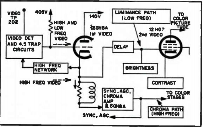
Fig. 42. Simplified first video amplifier circuit.
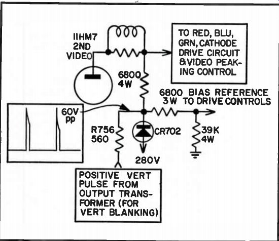
Fig. 43. Vertical retrace circuit.
VERTICAL BLANKING CIRCUIT (TUBE TYPE)
This tube type vertical retrace blanking circuit is found in many small screen RCA color TV receivers.
Operation of the Vertical Blanking Circuit
Vertical retrace blanking is accomplished in the plate circuit of the second video amplifier. Illustrated in Fig. 43 are the components associated with the vertical blanking operation. Let's now take a closer look at this vertical blanking operation. During active scan time CR702 is biased on (conducting); during vertical retrace time, a positive pulse from the vertical output transformer is fed through R756 to the diode. The 60 volt positive pulse is sufficient to bias off the diode. During the blanking interval, the positive voltage pulse is added to the plate voltage of the 11HM7 tube and coupled to the cathode circuits of the picture tube, driving the cathodes more positive-cutting off the picture tube during retrace time.
Several important points should be remembered when signal tracing the video circuitry through the 11HM7 tube stage. The video signal at the grid of the tube is altered by the insertion of the horizontal blanking pulse.
When the grid waveform is viewed at a horizontal rate on the scope, an additional negative pulse will be seen in the sync area of the waveform.
Likewise, the plate circuit waveform (at a horizontal rate) will contain the added pulse during blanking time. The amplitude of the pulse at the plate will be determined by the setting of the brightness and contrast controls.
When the plate waveform is viewed at a vertical rate, a positive excursion of the waveform will be noticed in the waveform area associated with the vertical blanking time. It should be noted that both the vertical and horizontal blanking areas will be altered from the output of the second video amplifier to the cathode of the color picture tube.
Points of Service
The most common faults in this blanking circuit would be loss of the vertical blanking pulses at the CR702 diode due to an open R756 resistor or defects in the vertical sweep stage. Also, an open or shorted CR702 diode will cause loss of vertical blanking and bright retrace lines will show up on the screen of the picture. Use the scope to look for low amplitude, distorted pulses or complete loss of these vertical blanking pulses in this stage.
COLOR DIFFERENCE AMPUFIERS (TUBE TYPE CIRCUIT)
These tube type color difference amplifier circuits are used in many small screen RCA color TV receivers.
Circuit Operation
These color amplifier stages have several unique features as shown in Fig. 44. Note that the R -Y, G-Y, and B-Y amplifiers operate in the grounded cathode mode, with grid taken from the blanker circuit. Also, note that only capacitive coupling is used from the output of the difference amplifiers to the grids of the picture tube.
The DC reference level for the color grids is established using a clamp circuit. Each grid (red, green, and blue) has an associated clamp diode to provide the DC level for the grids of the picture tube.
Notice the symmetrical appearance of all three amplifiers up to and including the path to the picture tube control grids. The cathodes are grounded and grid-bias voltage is obtained from a divider network connected to the negative voltage available at the blanker grid circuit.
The plate output circuit of each amplifier has basically the same configuration. The connection from the blanker grid circuit to the common grid circuit of the difference amplifiers sets the grid bias for the amplifiers.
In other color difference amplifier circuits the blanker plate pulse is applied at the cathodes of the difference amplifiers, setting the operating point, restoring DC, and providing horizontal retrace blanking.
Key Points of Service Check for correct B+ on plates of all color difference amplifier stages.
If not correct look for plate resistors that have changed in value (opened or increased in resistance) and any leaky by-pass capacitors or shorted spark-gaps that may be found in some circuits.
Shorted clamp diode will cause picture to be all one color. An open clamp diode may cause picture brightness to vary.
Check and make sure you have the proper negative bias voltage from blanker stage applied to control grids of the difference amplifiers.
If one color is missing, check for a faulty .01 uF coupling capacitor or open choke coil that feeds chroma information from the "X" and "Z" demodulators to the color difference amplifiers.
Make sure, with the scope, that you have the proper negative horizontal pulse from the blanker stage being fed to the DC clamp diodes.
TV SOUND CIRCUIT (SOU D-STATE IC)
This TV audio circuit is used in RCA's CTC-85 color chassis and several other models. The complete sound system is contained within one chip.
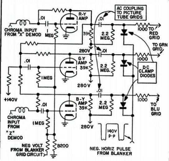
Fig. 44. Color difference amplifier circuits.
Circuit Operation The 4.5 MHz sound information developed by the combination sound detector/AFT discriminator chip in the IF module is fed to the sound module circuit as shown in Fig. 45A. This circuit demodulates the 4.5 MHz sound signal and amplifies the recovered audio to a power level that will drive the 32 ohm speaker. The customer volume control also interfaces with this sound circuit.
As shown in Fig. 45B, 4.5 MHz sound and audio processing is performed in a single integrated circuit chip, U-1. For simplicity of explanation, the device is illustrated as two sections - "U-1A" and "U-1B". The 4.5 MHz sound information is coupled to a double tuned transformer (Ti) via a coupling capacitor Cl. It is then applied to section U31A which amplifies and demodulates the information. The audio information is then coupled to the audio preamp and power stages in section "U-1B" through R1 and C8. The customer volume control applies variable DC bias to the gain controlled stages in the preamp to allow adjustment of the audio level.
Capacitor C24 (part of the speaker connector) provides the desired tone control characteristics. The power amplifier of U-1B furnishes a maximum power of approximately 1.5 watts (5 % distortion) audio which is coupled to a 32 ohm speaker via capacitor C13.
Points of Service
For complete loss of sound check for +27 volts DC to the module. If this voltage is correct then check the speaker voice coil, as it may be open.
The next check point is to see if you have correct 4.5 MHz sound signal input into capacitor C10.
For low or distorted sound suspect the U1 chip, the L1 coil or the T1 transformer. Also, check alignment of coil Li and the Ti transformer.
SYNC SEPARATOR CIRCUITRY (SOLID-STATE)
This sync separator stage is used in the RCA all solid-state CTC-40 color TV chassis.
Circuit Operation
A simplified schematic of this sync separator circuit is shown in Fig. 46. Sync pulses appearing at the collector of the noise inverter stage are coupled to the sync separator amplifier. This stage provides a signal of the correct polarity to drive the sync separator circuit.
The sync separator is a PNP common emitter "switch" which is pulsed into conduction by the negative going sync pulses coupled to its base by capacitor C312. Resistor R358 provides a discharge path for this capacitor. The output of the sync separator consists of positive going sync pulses which are applied to the vertical and horizontal deflection sweep circuits.
The noise immunity of the sync separator system is optimized during horizontal sync time by the use of a relatively small coupling capacitor, C312 (.01 µF) between sync stages. However, at the frequency of the vertical sync pulses, the impedance of C312 is too large to hold the sync separator in saturation throughout the pulse interval. The initial part of the vertical sync is enough, however, to charge C312 sufficiently to forward bias diode CR309. This action effectively clamps capacitor C357 across C312, providing a lower impedance path for the vertical sync pulses.
Capacitors C357 and C356 provide filtering for high video and chroma frequency information.
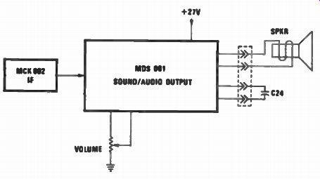
Fig. 45A. Block diagram of IC sound circuit.
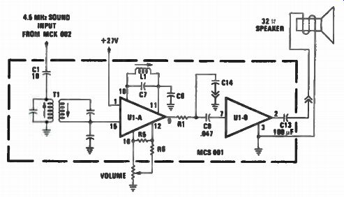
Fig. 45B. Simplified schematic MDS 001.
Points of Service:
Use the scope to trace the sync pulses throughout the sync separator circuit. Check for the correct vertical sync pulse output and the correct horizontal output pulse from this stage.
A defect in this stage can cause both the horizontal and vertical picture lock to be lost or just the vertical or horizontal lock to be lost.
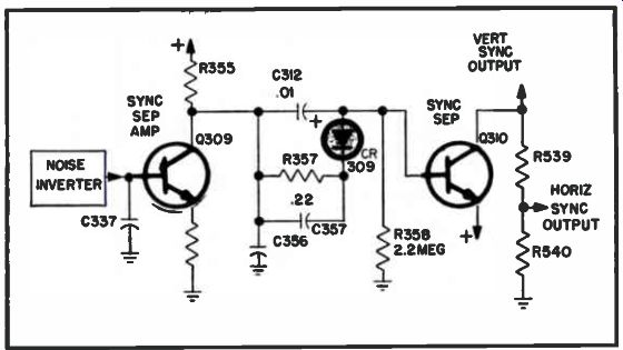
Fig. 46. Transistor sync separator circuit.
Check for proper DC voltages to Q309 and Q310 transistor stages.
Next, check transistors Q309, Q310 and diode CR309.
Look for value changes in resistors R539, R540 and leakage in capacitors C312 and C35.
AUTOMATIC GAIN CONTROL (AGC) CIRCUIT (SOLID-STATE)
This all solid-state (transistor) automatic gain control circuit is used in RCA's CTC-40 color TV chassis.
AGC Circuit Operation The function of the AGC system is to maintain a relatively constant video detector output over a wide range of TV station input signals. Thus, changes in video signal amplitudes are translated into DC voltages which are used to control the gain of the RF amplifier and IF stages.
Video information from the first video amplifier is fed to the gated AGC amplifier which produces a DC voltage proportional to the sync tip amplitude. The sync pulse is the only constant voltage level in the composite video signal that changes only when the signal input to the TV receiver changes. This DC AGC voltage is filtered and applied simultaneously to the RF AGC clamp circuitry and the IF AGC inverter stage.
Gated AGC Amplifier
A simplified drawing of the gated AGC amplifier is found in Fig. 47.
Video information with positive going sync pulses (level proportional to picture-carrier strength) is fed to the base of the gated AGC amplifier transistor. This transistor is made to conduct only during sync pulse time by positive going "keying" pulses coupled to the collector by capacitor C1.
These keying pulses occur at a horizontal rate and thus key the transistor on simultaneously with the horizontal sync pulses contained in the video information fed into the base. The bias on the transistor is kept low to allow the base emitter junction to become forward biased only during the positive peaks of the sync pulses. This optimizes the noise immunity of the amplifier.
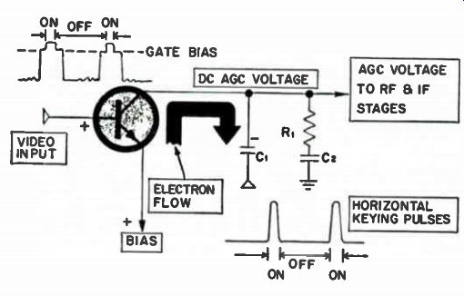
Fig. 47. Gated AGC amplifier circuit - simplified.
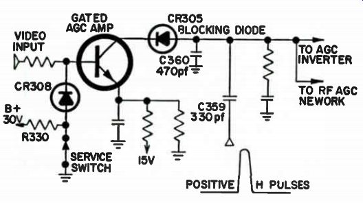
Fig. 48. Gated AGC amplifier circuit.
When the transistor conducts, electrons flow from the emitter to the collector, leaving a negative charge on capacitor C1. This negative voltage thus becomes the AGC voltage. Its true value will now be proportional to the amount of amplifier conduction, which in turn is determined by the peak positive amplitude of the incoming sync pulses. The RC network consisting of R1 and C2 improves the overall stability of the AGC system.
A more complete schematic of the gated AGC amplifier is shown in Fig. 48. In order to produce a blank raster for picture tracking set-up, a positive voltage is fed to the AGC amplifier by the action of the set-up switch. When the set-up switch is open this allows the positive 30 volt potential normally dropped across R330 to forward bias diode CR 308 and appear on the base of the AGC amplifier. This voltage will then saturate the transistor, producing a highly negative AGC voltage which cuts off the RF and video IF stages. This action removes the video information from the screen, which in turn causes a blank raster. A diode, CR 305, is placed in series with the collector of the gated AGC amplifier to prevent the developed negative AGC voltage from discharging back through the collector-base junction between keying pulses.
Key Check Points for Gated AGC Stage
Use a scope to check for proper video signal at base of the gated AGC amplifier stage.
With the scope check for the horizontal keying pulses that are fed to the collector of gated AGC stage via the C359 coupling capacitor. If the above two signals are not present or correct the gated AGC stage cannot operate properly.
Check for the +15 volt DC bias at the emitter of the gated AGC stage.
Suspect the following components if you have an AGC problem in this chassis: The AGC amplifier transistor, diode CR305, diode CR308 and coupling capacitor C359.
AGC CONTROL SYSTEM (SOLID-STATE TRANSISTOR)
This AGC circuit is used in the Sylvania E09 all solid-state color TV chassis.

Fig. 49. Transistor AGC circuit.
AGC Circuit Operation
Referring to the circuit in Fig. 49 we see that this AGC system consists of video inverter stage Q414, AGC comparator stage Q416, buffer stage Q202, and tuner AGC inverter stage Q203.
Transistor Q414 is driven by noise free video from IC400. This stage inverts and reduces the amplifier of the video to provide proper drive for the AGC comparator, Q416. The AGC comparator stage collector is ungated, and powered by a floating DC voltage developed by T400 sweep transformer pulse winding at pins 1 and 2, diode SC460, and capacitor C452. This stage compares the negative most portion of the composite video signal (usually the tip of the sync) and the DC voltage on the emitter, determined by the AGC control setting, R900. The comparator, Q416, controls the amplitude of the current pulse to filter capacitor, C217, and likewise, the voltage across it. This voltage is buffered by emitter follower, Q202, and is used to control the gain of the IF and tuner to maintain a constant tip of sync voltage at the base of Q416, the transistor comparator stage.
For signals from 10 microvolts to about 1.5 millivolts, the IF AGC controls the gain, and the tuner AGC controls the RF gain. IF gain decreases as the applied voltage from R217 increases, until diode SC210 is cut off, at this point IF gain is at minimum. Now, the tuner becomes the gain control factor. The RF stage is an FET and requires a voltage range from 10 volts to about 1 volt for maximum to minimum gain reduction.
Transistor Q203 provides the necessary inversion and level shifting for the FET tuner. Gain control above a few hertz or flutter is accomplished entirely by the IF stages. The combination of R226, R227, R1250 and C1250 components eliminate most of the AC signal and removes the tuner from the AC control loop. Capacitor C216 and resistor R218, provide the path for the AC component when diode SC210 is cut off. In this AGC system, further AC gain reduction is available from the IF beyond the minimum DC gain. This action is due to C215 and R215. These components are used to lower the AC loop gain at near maximum IF gain.
Points of Service
Keep in mind that this is not a keyed AGC system. The pulses from the winding on T400 are only rectified by diode SC469 and the floating DC voltage applied to the collector of Q416, AGC comparator.
Check with the scope for a correct video signal at the base of Q414 inverter stage.
Check for faulty transistor and diodes. Then check for the proper DC voltages on these transistors.
Remember, that a fault in the IF stages may cause a symptom that looks like an AGC trouble.
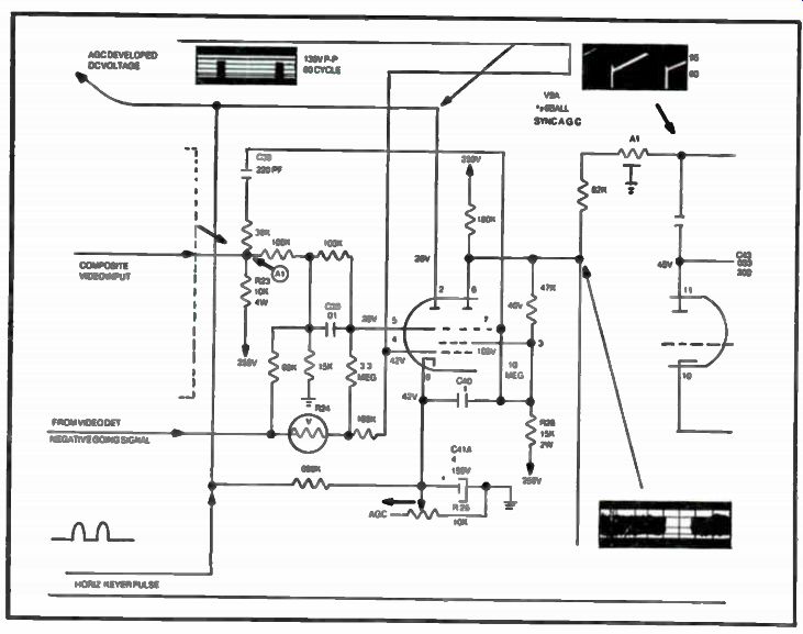
Fig. 50. Tube-type sync/AGC circuit.
SYNC AND AGC CIRCUITS (TUBE TYPE - ZENITH)
This sync/AGC circuit was used in many models of Zenith tube-type color TV sets. This BA 11 tube circuit is probably one of the most interesting sync/AGC systems in common use at this time.
Circuit Operation (Sync/AGC)
Referring to the 6 BA 11 circuit in Fig. 50, you will note a composite video signal, fed from the detector, has negative-going sync pulses and they are fed to pin 4. This signal usually is low in amplitude, and when noise free, has little effect on tube conduction. When noise pulses appear, a negative-going noise spike sends the tube deeper into cutoff for the duration of the noise spikes and prevents distortion of sync pulses at pin 6.
The average conduction of the sync operating point is set so that only the upper 30 percent of the video signal brings the tube out of cutoff, permitting only sync pulses to appear in the output. Note that pins 3, 6, 7, and 8 all are common to the AGC section of the BA 11 tube. As the control in the cathode circuit is set for minimum resistance, grid bias between 4 and 8 goes more positive and the tube conducts more. Thus, the AGC voltage at pin 2 (plate) goes more negative and is applied to the video W grids, causing IF cutoff.
When the AGC control is rotated clockwise, causing more cathode resistance, the bias is more negative and tube conduction is less. This reduces the negative AGC bias on the video IF's, and will cause the IF's to overload. During cutoff or overloading of the IFs, video is blacked out and does not reach the sync-input gm at pin 7, which will affect operation of the sync-separator section.
Circuit Checks and Tips
The secret in troubleshooting this complicated circuit is to find out which section is defective, as one fault usually masks the other sections operations. The cathode (pin 8) and first grid (pin 4) are common to all sections of this stage. This first grid is part of the noise cancelling circuit.
A good way to start checking is to short together pins 4 and 8 with a clip lead. ff the set now operates, the trouble is in the noise cancelling circuit.
Now check the video signal "back up stream" with the scope to find the problem. Also check the DC bias voltages, ff the set still refuses to work, leave the jumper in place and check the AGC section next.
The AGC section is comprised of plate pin 2 and the two other grids on the left side of the 6 BA 11. Instead of a constant B+ voltage, this plate receives a pulse (keyer) from the horizontal sweep transformer. For AGC voltage to be developed, video information with sync pulses must be found at the grid pin 5. This part of the tube conducts only when the keying pulse at the plate coincides with the horizontal sync tip pulses at the grid. Thus, the AGC voltage is developed on the basis of the horizontal sync pulses amplitude. Use your scope to see that the horizontal keyer and sync pulses are present and correct.
For sync troubles, check for correct DC voltage at plate pin 6 and also scope this plate and grid pins 3 and 7 for the correct sync pulses.
A dual-trace scope is very effective for testing this sync and AGC circuit system. There are several video, sync, and keying pulses fed to and from the plates and grids of these circuits, and all pulses must be of the correct phase and amplitude or this stage cannot function properly. By using a dual-trace scope, two pulses can be monitored simultaneously for correct timing, phase, amplitude and waveform.
While adjusting the AGC or noise-cancellation control, and at the same time viewing these pulses on the scope, lots of service information can be obtained. If the set has no picture or sound, and if AGC trouble is suspected, the first procedure would be to clamp the AGC line. If there is any video still present, then proceed with the scope checks. If the set has no picture (no video signal to CRT grids) it is almost a sure bet there aren't any sync or video pulses present at the sync/AGC tube elements. Should sync or video pulses not be found at the plates or grids, you may wish to inject pulses from a TV analyst in order to obtain some sort of picture on the screen of set under test. If partial operation can be attained, the scope can now be used to further pinpoint the faulty circuit stage or component.
ZENITH SYSTEM 3 ELECTRONIC POWER SENTRY AND HORIZONTAL SWEEP SYSTEM
All of these new Zenith circuit features are located on the 9-160 module that can be repaired or replaced. The 9-160-03 module is used in the 13, 17, and some 19 inch screen size sets. The 9-160-04 module is found in most 19 inch sets and all 25 inch screen size receivers. As we look at and see how to troubleshoot some of these very complex and unique circuits you may wish to refer to the complete diagram of the 9-160-03 module that is shown in Fig. 51. This self-regulating horizontal sweep and power system provides AC line and load regulation without using a power transformer and is thus called an Electronic Power Sentry.
A block diagram of this Electronic Power Sentry system is illustrated in Fig. 52. A line operated 150 volt DC power supply provides the energy to a horizontal pulse-locked chopper. The chopper regulates the voltage and drives the sweep and High Voltage transformer with a constant pulse. The HV transformer also supplies all the regulated voltages to the rest of the set with a scan rectification scheme.
The "key" to the new regulation system is the pulse width modulation (PWM). The line and load voltages are sensed by the PWM which controls the chopper rate by varying the "on time" of the chopper, and therefore, the supply voltage.
The main point to keep in mind when servicing this chassis is that the voltage for operating the entire set are derived from the sweep transformer.
Circuit Operation
As the block diagram indicates, the 150 volts DC B+ is regulated by the pulse width modulator and horizontal output transistor. As the B+ increases, the PWM decreases the "on time" of the horizontal driver, decreasing the stored energy and keeping the sweep voltages constant. As the B+ decreases, the PWM increases the driver "on time", increasing the stored energy and maintaining a constant voltage at the sweep stage outputs.
The Chopper Circuit
As we look at Fig. 53 let's see how the chopper circuit is used in the electronic power system. Figure 3-53 shows a pulse-width-modulated energy storage step-up converter/regulator. The AC line connected bridge rectifier and filter provide a voltage to the primary of the chopper transformer TX3301. The horizontal output transistor, QX3326, which is in series with the primary of TX3301,controls the stored energy by varying the "on time" inversely to changes in B+. If the B+ decreases, the "on time" must decrease, to maintain a constant current level. For a constant energy, current must be constant. The secondary winding of the transformer provides the step-up and phase inversion. During conduction of the transistor QX3326, the polarity across the secondary goes negative to positive. The negative voltage at the anode of the load diode CR3308 prevents its conduction.
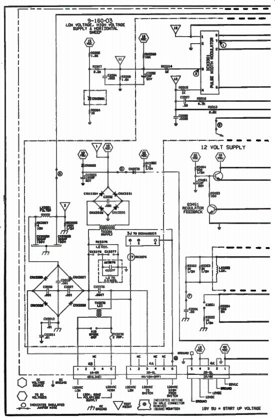
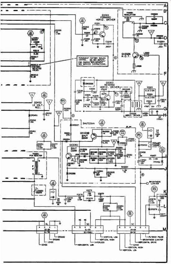
Fig. 51. Complete schematic of the 9-160-03 module.
After the QX3326 transistor turns off, the voltage on the primary reverses. Thus, the secondary voltage also reverses, forward-biasing the load diode CR3308 and charging the load capacitance. The voltage at the load capacitance is sensed and fed back to the Pulse Width Modulator (PWM) ICX3301. The PWM varies the base drive, inversely proportional to the load voltage variations. This in turn provides the regulated load voltage. The peak "off" voltage of the transistor is also inversely proportional to the "on time."
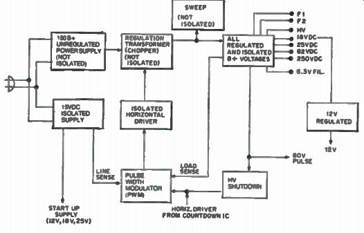
Fig. 52. Block diagram of the Electronic Power Supply.
Self-Regulated Sweep System
The circuits shown in Figs. 3-54 A & B are of the somewhat simplified regulator and horizontal output. The combination and further simplification of these two circuits evolved into the self-regulator, and is shown in Fig. 54C.
In the combined, evolved circuit, the transistor is removed from the sweep circuit, and will now operate as a chopper transistor. The load diode CR3308 is returned to the retrace capacitance. Since the drive power is supplied by the load diode, the B+ at the sweep decoupling capacitor, C3321, is not required. Since the chopper and sweep operate through a common transistor, there must be isolation during damper time. The isolation is provided by a diode CR3306 between the damper diode CR3307 and the transistor QX3326, the horizontal output. The diagram and waveform illustrations in Fig. 55 show the combination circuit in operation. After the completion of retrace time, the PWM is prepared to decide how soon the transistor will "turn on", to begin the energy storage process mode. For normal operation, the transistor turns on about 18 microseconds after retrace time, until the end of the trace. The "turn-on" time will vary from 5 to 30 microseconds after retrace. This time variation compensates for AC line to load variations as they occur.
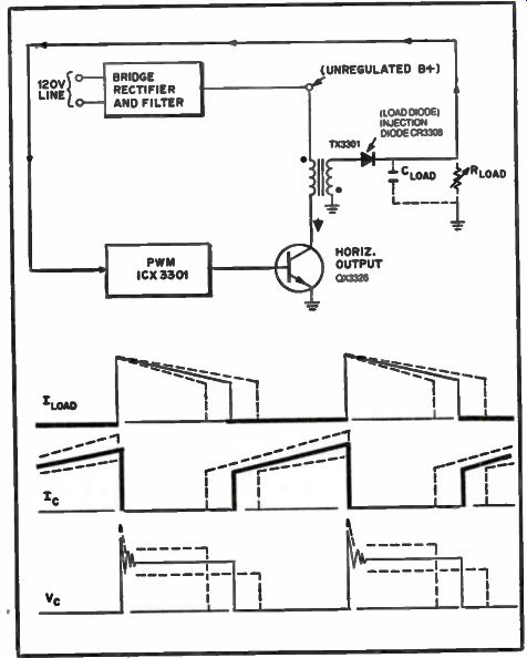
Fig. 53. Chopper circuit and waveforms.
The transistor QX3326 is "on" for the chopper operation during damper time. The diode CR3306 from the damper to the transistor, called the blocking diode, is reverse-biased until the damper is off. When the damper cathode goes positive, the blocking diode is forward-biased, clamping the yoke voltage via the transistor QX3326. The current through the transistor is a composite of the chopper current and positive yoke current. The transistor "turn-off " starts the retrace time.
Figure 56 shows the start of retrace. The transistor, QX3326, damper, and blocking diode are "off ". The voltage at the collector of QX3326 rapidly goes positive due to the inductive kick of the regulator transformer. The polarity reversal for the primary of the regulating transformer is also seen on the secondary. The positive voltage at the anode of the load diode CR3308, referred to as injection diode, forward biases the diode into conduction.
The retrace is produced by the resonant circuitry in the deflection circuit. The injection diode CR3308 is forward-biased because the anode voltage is increasing faster than the cathode voltage. The injection current aids in charging the retrace capacitance to a constant peak voltage level.
This helps to add the lost power. Also, the injection circuit continues to supply energy during retrace time. Thus, the injection diode CR3308 continues to conduct until the pulse width modulator restarts the transistor with a requirement for more power.
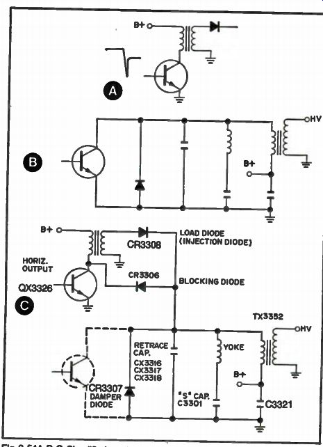
Fig. 54 A-B-C. Simplified regulator and horizontal output circuit.
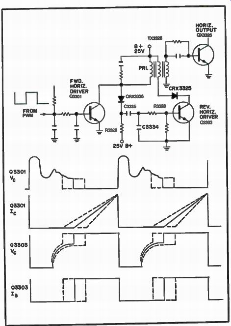
Fig. 55. Evolved chopper circuit and waveform.
The In-Phase Driver
The driver in the conventional sweep circuits is part of an out-of phase system. For example, when the driver is on, the output transistor is off, and vice-versa. This system has an energy storage circuit storing energy during conduction, and supplying output base drive during the off time of the QX3326 transistor.
In the self-regulation-system, the driver is part of an in-phase system. When the forward driver Q3301 turns on, the output transistor also turns on. The driver circuit is powered by the 25 volt supply, which allows for a low resistance primary winding on the driver transformer TX3326. The closely coupled secondary winding is directly driven by a current ramp. The inductive impedance and low resistance provide for a very efficient driver circuit. The direct-drive produces a constant drive level independent of the duty cycle. The conventional sweep circuit with the out-of-phase drive system requires a minimum "on time" to turn the output transistor "on" at low line voltages, and produces excessive drive current at high line voltages.
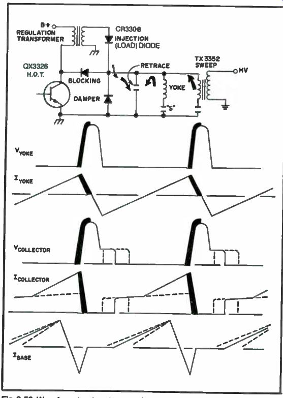
Fig. 56. Waveform drawings for start of retrace.
One disadvantage is the negative drive current which is unacceptable for a fast fall time in the output transistor. To maintain a fast fall time in the output transistor, a reverse driver transistor Q3303 is added to this circuit. The forward driver transistor Q3301 is driven by the pulse width modulator IC and the reverse driver transistor Q3303 is driven by the collector voltage of Q3301.
A diode CRX3336 and resistor R3329 form a clamp circuit which clips (or clamps) the peak of the collector voltage of Q3301. The waveform is decoupled by capacitor C3335. A capacitor C3334 and resistor R3328 form an integrating network which shapes the signal that drives the base of Q3303. Transistor Q3303 turns "on" after Q3301 turns "off". The current through Q3303, flowing through the primary of TX3326, drives the base of the output transistor, QX3326, negative, providing a "clean" output pulse to switch QX3326 in about 0.5 microseconds.
The Pulse Width Modulator
Now, let's look at Fig. 57 which shows the schematic of the pulse width modulator and the internal circuit of the PWM IC. Pin 3 is connected to a reference voltage, while pin 4 is driven with a triangle waveform.
When the triangle wave reaches a larger amplitude than the reference voltage, Q9 and Q10 will steal current from Q11 and Q12 from the current source Q13. The action of Q10's conducting will cause Q6 and Q7 (a positive feedback switch) to snap-on. Transistor Q5 is an in-phase current mirror of the Q7 collector current. Therefore, Q5 will also turn on, feeding a large current into the base of Q3 which, in turn, will also overdrive Q1, the output device. The result will be a square wave output, starting and ending where the triangle waveform crosses the reference voltage applied to pin 3.
Let's dig in a little further now and see how this is used in the electronic regulator system.
Going back to Fig. 57, note that pin 7, of the PWM IC receives the "H" drive pulses from the "countdown IC" 221-103 located on the M2 module. When troubleshooting this sweep system this is a good scope check-point to look at to see if these "H" pulses are present and correct.
These pulses (note correct waveform in Fig. 59) are coupled to the base of Q14, an overdriven amplifier, which amplifies and clamps the "H" pulses between ground and B+, producing a 12 volt P-P square-wave.
This square-wave exits the PWM at pin 6 and is then shaped by R3316, C3307, and C3306 to a triangle and coupled to pin 4, along with a DC reference voltage from R3317, R3312, and R3310 to the same point. On the other half of the differential comparator (pin 3) a sample of the voltage from the 15 volt, 60 Hz power supply, and a sample of the 18 volt sweep derived power supply are mixed. If either supply varies, the resultant square-wave output will vary in duty cycle, providing pulse width modulation. The actual transfer graphs for some typical voltage changes are shown in Figs. 3-58 and 3-60.
To visually illustrate the action of the pulse width modulator, refer to the dual-trace scope pattern shown in Fig. 61. These waveforms were taken at the base of the forward driver transistor Q3301 which is indicated as scope check point 4 on the full schematic shown in Fig. 51. The top trace occurred when the AC line voltage was at 130 VAC and you will note the pulse is narrow. Now the bottom trace widens out as the AC line voltage goes down to 75 VAC. Thus, a good example of the PWM in action.
Now, once again, return to Fig. 57. Look at pin 8 of the IC, which is marked "Flyback Pulse". This input can stop the square-wave from appearing at the output of the PWM at pin 1. It is used to prevent the PWM from turning on the driver and, hence, the horizontal output transistor from turning on, during flyback when the collector voltage is high. This input is also used to shut down the system if the high voltage becomes too high.
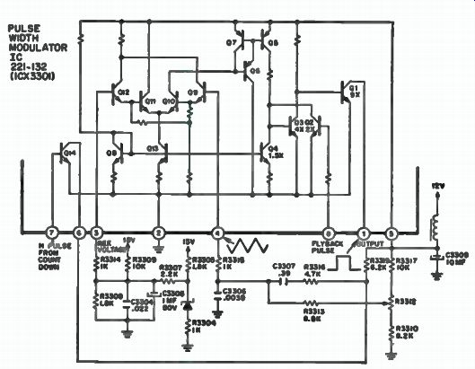
Fig. 57. Pulse width modulator IC.
AC Line Power and Kick Start Comments
This system has a 150 volt unregulated power supply and a 15 volt DC isolated power supply. All power for the receiver operation is derived from the unregulated AC line-connected 150 volt B+. This also includes the CRT filament. Don't try to measure any of the AC supplies from the sweep transformer. However, the DC voltages can be easily measured during any troubleshooting procedures.
The term "line-connected" B+, or "line-connected" ground, indicates no isolation from the AC line.
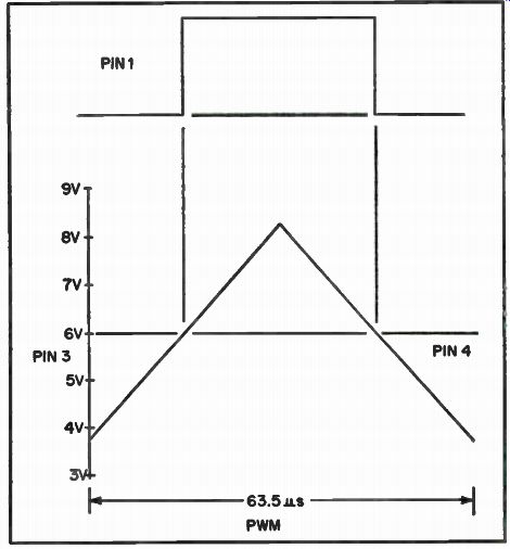
Fig. 58. Transfer graph.
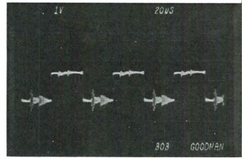
Fig. 59. Correct "H" pulse to PWM IC.
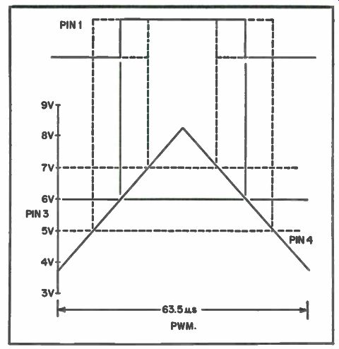
Fig. 60. Variations of transfer PWM characteristics.
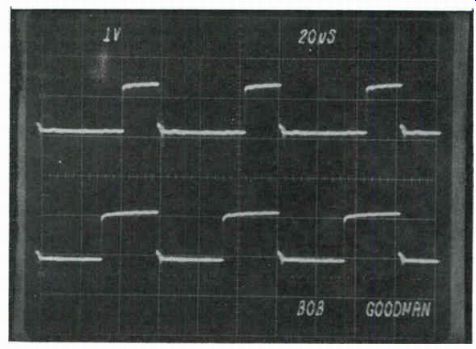
Fig. 61. Scope pulse illustration of pulse width modulator in action.
Keep in mind that the 15 volt supply is used only as a reference of the 60 Hz supply line voltage by the PWM at pin 3. The 15 volt supply is isolated from the AC line by transformer TX3351.
The power supply section is protected against lightning spikes or surges with an air spark gap, and a fuse for any short circuits that may develop.
High Voltage and Excessive Load Shut-Down
A shut-down circuit is used for X-ray and HV sweep breakdown protection and goes into operation only if the high voltage increases by 4 to 6 kilovolts. Also, if an excessive load (current) exists or if the potential difference between the "hot" and "cold" grounds becomes excessive, its effect is to shut down the entire receiver by cutting off the horizontal stages.
This module contains a 12 volt regulator, a 32 volt current source, scan rectification circuits that produce 62 volts DC, 25 volts DC, 18 volts DC, 250 volts DC and voltage for the picture tube filaments.
Circuit Modification for Horizontal Output Transistor Failures
Remember, when a 9-160 module fails there can be various causes of horizontal output transistor failures other than a defective transistor.
One case, which is probably the most common, is intermittent or total loss of base drive. This may well be caused by poor contacts of the intermodule connector plugs or other component failures such as the 221-105 IC (loss of the 503 kHz oscillator), 221-103 IC (loss of the count-down process), or 221-132 (faulty PWM IC), or even components associated with these IC's.
Since this type of failure can be due to any of several other faults, a new circuit has been incorporated in the 9-160 module which protects the horizontal output transistor. However, if a horizontal output transistor has failed, check for an intermittent contact of the inter-module connector plugs.
In this new circuit, (see Fig. 62) a transistor (121-973) is placed across pin 8 of the pulse width modulator (PWM) IC 221-132 to ground.
The transistor turns on when the 8.2 Zener diode conducts. Thus, pin 8 is grounded through a 47K resistor once start up has occurred. If the horizontal drive signal should now be lost, the horizontal sweep circuit will squeg at a safe rate and will prevent overstress of the horizontal output transistor.
Another cause of horizontal output transistor failure is a loss of "off drive" which is the signal or current necessary for a fast cut off time, incorrect or loss of the base current. The base current of the horizontal output transistor is due to the function of the reverse driver stage. When a horizontal output transistor is replaced, the base drive signal should be checked. The primary reason for loss of base current is a faulty reverse driver transistor or a reverse driver base clipper diode CR3336. It may be difficult to check the base current when the horizontal output transistor has been changed. So, it is important that at least the base voltage waveform be checked for correct shape and amplitude as the system may function properly for long periods of time before the horizontal output transistor fails again.
Another cause of output transistor failure may be caused by a breakdown of the heat transfer grease. In some cases when some black arc track marks are visible, the horizontal output transistor may be good and only the grease has broken down.
In one case where the output transistor shorted and blew the fuse, a customer removed the back of the seat and shorted across the fuse and turned the set back on to watch his special program. However, not for long, as a loud noise made him pull the plug, quick. This shorted transistor caused the C3315 capacitor to blow-up and also burnt up the 6.8 Ohm R3323 resistor.
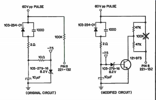
Fig. 62. Modification of horizontal output circuit.
Service Procedures and Tips (9-160 Module)
Use the following procedures for isolating the faulty module that will cause loss of (H) signal.
Turn the set on and check for presence of the 503 kHz (H) oscillator signal at pin 4 of connector 1B located on the 9-151 module. This will be a 1.5 P-P signal riding on a 2.5 volt DC level as viewed on the scope.
If this signal is incorrect or missing, replace the 9-151 module.
Now verify that the horizontal drive signal is present at pin 4 of connector 2B on the 9-152 module. This will be a 2 volt P-P signal riding on a 1 volt DC level.
If this signal is incorrect or missing, replace the 9-152 module. If all tests and modules have been OK up to this point then the 9-160 module is faulty.
Set Inoperative (Fuse Blown). When the fuse is blown on the 9-160 module, the cause could be the module or a short somewhere else in the receiver. A few checks with the ohmmeter should help locate the difficulty quite easily.
Make a resistance check on the Q3226 horizontal output transistor.
From the collector (case) to the heat sink you should have a reading of 3K ohms or more. A very low or zero reading indicates a shorted device.
Before repairing this module, make sure a failure of this output transistor was not caused by a defective 9-151 or 9-152 module.
Ohmmeter readings can vary due to a number of factors, such as the ohmmeter range used, the lead polarity, and etc. Always reverse the leads and use the low ohms scale to make these resistance readings.
Excessive Picture Brightness (Retrace Lines). The cause of this symptom is usually the loss of the +250 volts on the 9-160 module (probable faulty diodes) or a defective 9-155 (RGB video module). In some instances a defective 9-155 module will also damage the 9-160 module. A faulty picture tube will also give nearly the same symptom.
To prevent damage to a new 9-160 module, make the following checks before module replacement.
Check for the presence of +250 DC at pin 3 of connector 3C on the 9-160 module. If the voltage is OK, check for +250 volts at pin 2 of connector 5B on the 9-155 module.
If the voltage is correct, then replace the 9-155 module. If no voltage is found, turn the set off and measure the resistance of R3481, a 47 ohm resistor. If the resistor is good, replace the 9-160 module. If you find the resistor open, replace both the 9-155 and 9-160 modules.
Deflection Yoke Tips and Checks. Should the horizontal windings on the deflection yoke become shorted, the screen will go black, the HV will drop to about half value and the 2 amp line fuse will blow. At first it may appear as a faulty 9-160 module. One quick check is to remove the 3P yoke plug and jump a clip lead from pin 4 of the 3P plug to pin 3 of the 3D yoke plug. Now turn on the set and the high voltage will go up and you will see a thin white vertical line on the screen if the yoke was defective.
With the yoke plugged in and a scope connected to pin 1 of the plug 3D (hot lead) and the ground lead of the scope to pin 6 of the 3D yoke plug, the waveforms taken at this point by the scope can be used as comparisons to give you an indication of the yoke's condition.
The bottom trace in Fig. 63 is for a good yoke, while the top waveform indicates an open yoke winding condition. While in Fig. 64 the bottom trace is for a good yoke and the top trace indicates a faulty yoke that has shorted windings and has loaded down and detuned the sweep output stage.
Another place where you can make a scope check is on the 250 V DC supply pulse winding that is tap K on the TX3352 sweep transformer. A good pick-up point on the board is at the L3476 choke coil. A good yoke will give a pulse like that shown in the bottom trace of Fig. 65. An open yoke will produce a pulse as shown in the top waveform. A shorted yoke will give a very low amplitude pulse at this test point.
High Voltage Shut-Down Quick Check. To determine if the 9-160 module is in the shutdown mode, a quick and simple check can be made. Measure the DC voltage at pin 3 of connector 3C on this module. If the 9-160 module is in the shutdown mode a voltage of +8 to +9 volts will be measured at this pin. The normal DC voltage is +.9 to + 1.2 volts DC.
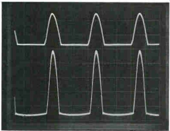
Fig. 63. Top pulse shows an open yoke, while bottom trace is for a good
yoke.
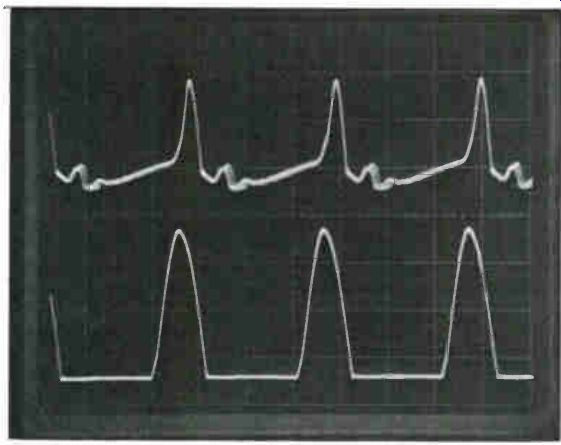
Fig. 64. Top trace Indicates a shorted yoke while bottom trace is for
a good yoke.
TV SOUND-SOLID-STATE IC (QUASAR TS-958 & TS-959 CHASSIS)
This IC sound system is used in the Quasar TS-958 and TS-959 color chassis. Most of the sound signal processing stages are within IC 201. This IC contains the sound IF/Limiter, detector, and two audio amplifiers (pre-amplifier and driver)stages.
Circuit Analysis
Referring to the circuit in Fig. 66, we see that capacitor C201 couples the picture and sound carriers from the third IF stage to diode D201. These signals beat in the diode to produce the 4.5 MHz FM sound IF signal which contains the transmitted audio modulations. This signal is fed through a selective tuned circuit to sound IF transformer 1201 which couples the sound IF to pins one and two of the IC. The 4.5 MHz sound IF signal is amplified and fed to the detector. The external quad coil between 9 and 10, shifts the phase of the sound IF signal 90 degrees. This phase shifted signal is also applied to the detector stage in the IC. The detected audio signal is amplified and leaves the IC at pin 8. Capacitor C212 couples the signal to the tone control, and C209 couples the audio to the volume control. From the volume control, C210 couples the signal to pin 14 of the IC and to the audio driver section. The driver of the chip, pin 12, direct couples the signal to audio output transistor Q201. These pre-amp and audio output driver stages are shown in Fig. 67. Forward bias for Q201 is developed within the IC, and the amplified audio signal at its collector is transformer coupled to the speaker. A diac across the primary protects the output stage transistor against any current transients developed in the transformer.
Sound IC Checks and Tips
Voltage checks and/or signal injection techniques can be used when troubleshooting this sound IC and its associated circuits. First check all supply voltages to see if they are correct. Then check any other voltages in the associated circuits. Use caution to keep the meter probe tips from slipping and shorting any adjacent terminal pins. This can quickly ruin a good IC. If all voltages are correct, then inject a low level signal at the input terminal pins, 1 and 2. Now, check the output of the chip with a scope for the audio signal. Another effective approach is to check the input and output of the IC with a scope for proper signals. These easy checks minimize the possibility of having to replace a good IC that could be damaged during removal.
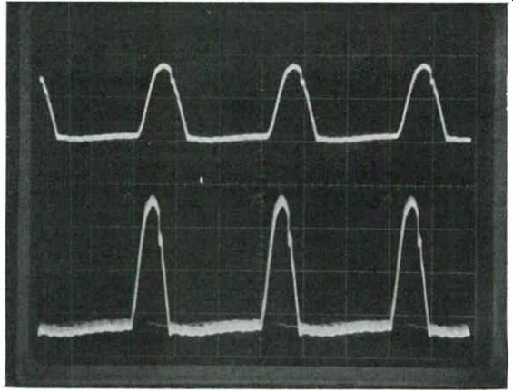
Fig. 65. Taken at 250 volt pulse winding on sweep transformer the top
trace indicates an open yoke. A good yoke gives a trace as shown in the
bottom wave-form.
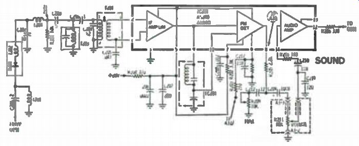
Fig. 66. IC IF/Limiter and detector circuit.
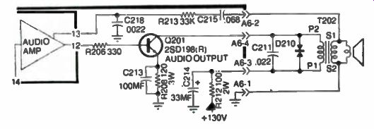
Fig. 67. Pre-amp and driver audio stage.
VERTICAL SWEEP SYSTEM (SOUD-STATE TRANSISTOR) QUASAR
This transistor type vertical sweep system is used in Quasar TS-958 and TS-959 color TV chassis.
Circuit Analysis:
The vertical sweep in this circuit is generated by altering the charge on capacitor (C457), very slowly during scan time and quickly reducing the charge during retrace time. The result is a sawtooth waveform that is presented to the base of driver transistor Q452 (Emitter Follower) which is passed on to the base of output transistor Q455.
Two NPN output transistors are stacked and share the B+ supply voltage. When in operation an average voltage (DC) develops across coupling capacitor C461.
The sawtooth voltage, applied at the base of Q455 controls its conduction, which inversely changes conduction of Q454. This type arrangement produces maximum current through the yoke at the top of the screen which decreases to zero at screen center then increases to a maximum in the opposite direction and moves the beam to bottom of screen. As the sawtooth cuts off Q455, the beam quickly retraces to the top and the process is repeated.
The complete vertical circuit Fig. 68, shows the positive feedback to the oscillator required to sustain oscillation. The same network provides negative feedback to the saw forming capacitor C457 to produce a more linear charge. Linearity correction is also enhanced by feedback from the emitter of output transistor Q455.
The amplitude of the sawtooth voltage developed by C457's charge is determined primarily by the height control (R456) adjustment.
The free running frequency of the oscillator is slightly lower than 60 Hz as determined by the vertical hold control. This allows the negative going sync pulse fed to the emitter of Q451 to lock the vertical oscillator to the TV stations transmitted sync pulses.
Diode D453 protects the base emitter junction of Q454 against excessive reverse bias voltages.
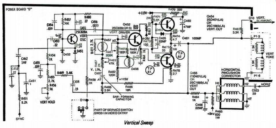
Fig. 68. Quasar transistor vertical sweep circuit
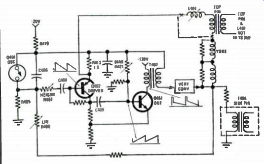
Fig. 69. Transistor type vertical sweep circuit.
Circuit Troubleshooting Tips:
Oscillation at the vertical rate is dependent on the feed-back from the output. Any thing that interrupts the path stops the proper charge/ discharge of the saw-forming capacitor. Voltage checks reveal most causes but a scope can be helpful in troubleshooting problems of vertical linearity and loss of picture sync.
VERTICAL SWEEP CIRCUIT - SOLID-STATE (QUASAR TS-951 CHASSIS)
This solid-state vertical sweep circuit is found in the TS-951 and other Quasar color TV chassis.
During retrace time C408 couples the surge of positive voltage at the emitter of Q401 to the base of vertical driver transistor Q402. Positive voltage to this PNP transistor turns it off, and its collector voltage drops.
Capacitor C409 couples the negative going voltage to the base of Q451, and drives vertical output transistor Q451 into cutoff. Its collector current drops to zero and the field in T402 collapses. This produces current in the secondary of T402 and onto the vertical windings of the deflection yoke.
This vertical circuit is shown in Fig. 69.
At the end of retrace, oscillator transistor Q401 turns off and sawformer capacitor C406 starts to charge via R405. As this capacitor charges, voltage at the emitter of Q401 decreases, and C408 couples this negative going voltage to driver transistor Q402. The driver begins conduction and develops a positive voltage at its collector, which is coupled to the base of the output transistor to initiate conduction in this device. When Q451 begins conducting, current in the output transformer and deflection coils reduces slowly and the beams move downward to screen center. As the sawtooth voltage continues to increase conduction thru Q451, current in the output transformer secondary and vertical yoke coils reverses and deflects the beams linearly to bottom of the screen.
When the beams reach the bottom of the screen, the oscillator emitter voltage has dropped enough to let this transistor conduct and repeat the cycle.
It is essential that the free running frequency of the oscillator be slightly lower than 60 Hz, so vertical sync from the TV station will control it. Vertical hold control value determines this operating point. When a station signal is received C401 couples a negative going vertical sync pulse to the collector of Q401, and across the primary of 1401. The secondary couples a positive going pulse to the base of Q401, which drives it into conduction. Height control R407 varies the amplitude of the sawtooth voltage to the base of the driver transistor, thus it controls vertical size.
Feedback from the vertical output transformer provides wave shaping to obtain good linearity. D402 and C412 protect the output transistor in the event the transformer secondary or vertical windings in the yoke open.
The vertical bias circuit compensates for driver and output circuit tolerances, and R421 is adjusted to obtain best linearity in the top portion of the screen. This control should not need adjustment unless component replacement is required in this circuit for repairs.