This Section covers the various circuits found in a color TV receiver. A description of each circuit followed by the diagnosis of symptoms and troubleshooting checks will help you first identify problems, and then effect repairs.
HORIZONTAL OSCILLATOR/VERTICAL COUNTDOWN SYSTEM
This circuit is found in RCA's CTC 99/101 color TV chassis. The circuit uses an integrated circuit (a computer-related chip U400) to perform the operations of horizontal oscillator and vertical countdown.
This combined countdown circuit feeds both the horizontal drive for sweep output and the vertical drive for the vertical amplifier. Note the block diagram of the countdown circuit in Fig. 1.
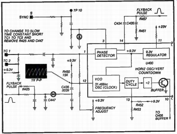
Fig. 1. Horizontal count-down block diagram.
A horizontal rate output pulse is fed from pin 10 of U400 to the horizontal buffer Q406. The buffer stage then drives the driver stage and then the horizontal sweep stage. A vertical rate output pulse is available at U400, pin 8 (TP 9) and is applied to vertical sweep transistor Q500. The vertical pulse triggers the sawtooth transistor developing the ramp signal for the vertical amplifier.
Composite sync is fed to the horizontal oscillator/vertical countdown circuit via terminal S. From this point it is differentiated to provide horizontal sync pulses to pin 3 of U400. The sync pulses can be checked at TP-10. The composite sync signal is also coupled through two stages of integration to develop vertical sync at pin 5. The two stage integrator allows this vertical countdown system to be compatible with most forms of nonstandard sync signals.
The oscillator/countdown circuit is powered from a +9.3 volt regulated supply. The regulator is located within the IC and is biased through a resistor from the +23 volt supply. Pin 11 of U400 is the source for +9.3 volts to circuits external to the chip.
Controlling the horizontal oscillator/vertical countdown IC operation is an internal voltage controlled oscillator (VCO) which develops the clock frequency for the IC. The clock runs at twice the horizontal frequency for reasons we will see a little later on.
The VCO in the IC oscillates at 31.468 kHz, which is exactly twice the horizontal rate. The frequency of the VCO is determined by R450, C436, and the frequency adjust control. The VCO frequency is modified by the phase detector, which is located in the IC. The output of the phase detector at pin 1 is filtered, then coupled to the input of the voltage controlled oscillator (pin 12). To correct this picture bending, the voltage at pin 12 is modulated by feeding a detected sweep error signal to a (.0039) capacitor, C436. This is similar to "anti-bending" circuits used in other chassis.
The output of the phase detector modifies the VCO to achieve frequency lock to the station's horizontal sync signal. The phase detector compares the frequency of the horizontal retrace pulses to that of the incoming horizontal sync pulses coupled from the sync/AGC circuit in the IF. The horizontal sync pulses are differentiated and fed to pin 3 of U400. These pulses are then compared with the retrace pulses which have been integrated by R457 and C435. The resultant sawtooth is coupled to pin 14.
The phase detector output DC voltage (pin 1) is fed to the VCO control input at pin 12.
The output of the VCO is coupled to a duty cycle adjustment circuit.
The duty cycle is determined by a fixed DC reference voltage at pin 13 of U400. The output of the duty cycle block is applied to a divide-by-two counter, in which VCO output frequency is divided by two to provide the horizontal driver with 15.734 kHz horizontal pulses. The output of the counter is coupled through an internal open collector buffer stage to pin 10.
At this point, the output voltage square-wave varies between zero and about 4 volts. This square-wave is fed to the horizontal buffer stage which amplifies the signal which is then fed to the horizontal driver stage.
Vertical Countdown System
The vertical countdown concept is based on the exact relationship between horizontal and vertical sync frequencies. There are exactly 262.5 horizontal lines per field. Division (countdown) by other than whole numbers is not possible in this system; therefore, division of the horizontal rate by 262.5 to provide the proper vertical-to-horizontal sync ratio is not possible. To allow for countdown by a whole number, it is necessary to double the horizontal rate of 15.734 to 31.468 kHz. The result is a ratio of 525 to 1. The master clock VCO in U400 oscillates at the required 31.468 kHz rate. The clock output is then divided by two to provide the horizontal driving pulses and by 525 to obtain the correct vertical pulses.
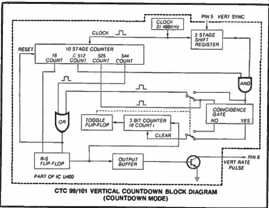
Fig. 2. Vertical count-down block diagram.
The vertical countdown system used in the RCA IC is a two mode system. One mode is the count-down operation, the other is for sync operation. The two modes of operation allow the system to be compatible with non-standard sync signals. The IC internally switches between the two modes of operation to match type of signal being received. Mode switching occurs after eight consecutive cycles of received vertical sync that is in phase, or out of phase, with the 525 count from the countdown system.
Standard NTSC Countdown Mode
The countdown IC uses counters, shift registers, coincidence gates, flip-flops, and other logic circuits to perform the necessary functions for countdown. The operation of the vertical countdown circuit operating in the countdown mode with an NTSC signal will be covered next. Refer to the vertical countdown block diagram in Fig. 2.
A 10-stage counter counts every clock pulse from the 31.5 kHz VCO. After counting 512 clock pulses, the greater than or equal to 512 count line goes high or to a logic 1. This places a logic 1 at one input of an AND gate.
The other input of the AND gate remains at zero until vertical sync occurs.
When vertical sync occurs, both inputs to the AND gate are ones, providing a 1 at the output which is supplied to one input of the coincidence gate. The other input of the coincidence gate is received from the 525 count line of the 10-stage counter. With the presence of an NTSC sync signal, the 525 count goes to a 1 at the same time vertical sync occurs.
This provides a 1 at both inputs of the coincidence gate causing a 1 to occur on the yes line of the coincidence gate. This 1 is applied to the clear line of a 3-bit counter (clearing the counter) thus keeping the toggle flip-flop from changing states.
In addition to feeding an input to the coincidence gate, the 525 count line data is also supplied to one input of a two-input OR gate. The output of the OR gate is coupled to an R-S flip-flop causing the output of the flip-flop to change state (set) generating a vertical pulse via the output buffer stage.
The pulse to the output buffer stage is also counted by the 3-bit counter.
The logic 1 pulse at the output of the OR gate is also coupled back to the reset line of the 10-stage counter forcing it to reset to a 0 count.
The 10-stage counter again begins counting the clock pulses. After it has counted the 16th clock pulse, the 16 count line goes to a logic 1. This line is connected to the R-S flip-flop, resetting the flip-flop; thus, the length of the vertical output pulse is 16 clock counts. As long as an NTSC signal is being received, the operation of the countdown remains in this mode. Therefore, on every 525th count, the countdown circuit checks for coincidence of the 525 count and sync. As long as coincidence occurs, the coincidence gate clears the 3-bit counter, allowing the 525 count to trigger an output pulse through the OR gate and R-S flip-flop, thus, completing the cycle.
If no vertical sync is being received by the countdown IC, the second input to the AND gate remains at logic O. This means that the one input to the coincidence gate stays at logic O. Therefore, when the 525 count is reached and applied to the coincidence gate, the coincidence gate develops a 1 on the no line and a 0 on the yes line. This will clear the 3-bit counter.
As before, the 525 count line energizes the R-S flip-flop through the OR gate. The flip-flop again drives the output buffer stage and also sets a 1 into the 3-bit counter stage. Also, the output of the OR gate resets the 10-stage counter to 0. Again, after 16 counts, the R-S flip-flop is reset, terminating the vertical output pulse. This cycle continues until the 3-bit counter counts eight occurrences of no vertical sync occurring which is indicated by lack of a good pulse on the yes line of the coincidence gate. After receiving the eight consecutive pulses without being cleared, the 3-bit counter energizes the toggle flip-flop which shifts the mode of operation from the countdown mode to the sync mode.
In the sync mode, vertical scan is initiated by the occurrence of vertical sync. If no vertical sync is present, the countdown circuit will run free. The OR gate, which triggers the output generating R-S flip-flop, has two inputs: the output of the AND gate, and the 10-stage counter 544 count line. With no incoming vertical sync present, the AND gate will generate no output pulses. Therefore, the OR gate will be activated by the 544 count line only.
Horizontal/Vertical Countdown Circuit Servicing
For the following service information refer to the circuit and scope waveforms shown in Fig. 3.
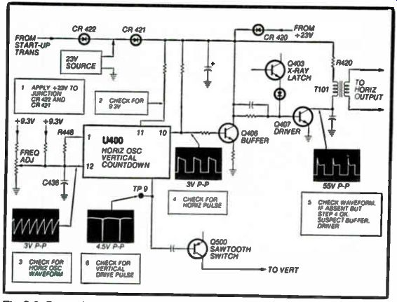
Fig. 3. Count-down circuit with waveform checkpoints
THE SYMPTOMS:
• No horizontal oscillator operations.
• Lack of horizontal or vertical sweep.
• Erratic horizontal operation.
• Erratic vertical operation.
• No vertical scan.
The Diagnosis
Without the horizontal oscillator in operation, no other circuits in the TV chassis will operate, hence, there is no secondary B+ supply. To check the operation of the horizontal oscillator, it is necessary to apply an external source of +23 volts to the cathode of CR422 with the set turned off. Use a battery to sub for this power supply voltage.
Service Procedure
Use an isolation transformer, disconnect the line cord during all static checks, and use insulated tools or clip leads for any dynamic checks.
If during servicing it is necessary to replace the horizontal/vertical IC (U400), a resetting of the horizontal frequency adjustment may be required. To reset this adjustment, short the sync input (TP 10) to ground and adjust the frequency control for a stable horizontal picture.
• No horizontal oscillator operation.
• Lack of horizontal or vertical sweep.
• Erratic horizontal operation.
With +23 volts applied to the cathode of CR422, check for approximately 9.3 volts at pin 11 of U400. This voltage is internally regulated by U400. Check for the horizontal oscillator drive output waveform at pin 10 of the U400 chip.
Check at the collector of the horizontal driver transistor Q407 for the correct drive waveform of 55 volts P-P. If the waveform is present at pin 10 of U400, but is not present at the collector, suspect a shorted Q407 transistor. If these circuits all check out good, then the problem may be in the horizontal start-up circuits.
Erratic Vertical or No Vertical Scan
Check for the presence of vertical drive pulses at test point TP-9. If the vertical pulse is present, the fault will probably be in the set-up switch or vertical amplifier.
VERTICAL SWEEP AMPLIFIER (SOUD-STATE) RCA 99/101 CHASSIS
The main B+ power for this sweep system is a +23 volts instead of a negative supply that has been used in earlier model SS RCA sets. The retrace-switch transistor is supplied with +55 volts providing the extra required B+. The base bias supply for the top and bottom output transistors and the retrace switch is developed through a resistor from the +210 volt supply.
Brief Circuit Analysis
This vertical sweep circuit employs a vertical height tracking circuit.
Height tracking is accomplished through R506, a 4.7M resistor, which is connected to the beam current detector via the X-ray protection/shutdown circuit. Q501's base bias is modulated by the beam current, causing the vertical amplifier output to "track" with changes in average brightness.
This maintains the proper aspect ratio between horizontal and vertical scan, preventing vertical "shrink" under high beam current conditions.
Vertical Amplifier Trouble Symptoms
• No vertical deflection
• Reduced scan
• Retrace lines at top of picture
Some Preliminary Checks
Pull set-up switch in and out a few times to make sure that the switch contacts are not dirty. Check for presence of vertical drive pulse at TP 9.
Check for correct B+ supplies: + 23 volts, + 55 volts, and + 210 volts.
The best way to service this vertical amplifier circuit is to place the service switch in the set-up position. This prevents the oscillator stage from having any effect on the vertical amplifier circuit.
Troubleshooting Procedures
Use an isolation transformer and disconnect the line cord during all static checks. Refer to the simplified diagram in Fig. 4 with the boxed service check points.
No Vertical Deflection
Check the Q501 error amplifier for a 30 volt bias supply at the base.
This voltage is developed in the X-radiation protection circuit and can be measured at the end of R506 away from the base of Q501. Without this voltage, the vertical amplifier will not operate. If this voltage is not present, check-out the X-radiation protection and shut-down circuitry.
Now check the midpoint voltage of the vertical amplifier stage at the collector of Q504. If this voltage is less than 12 volts, suspect a shorted transistor.
Next, check for 13 volts base bias at the collector of Q502. If 0 volts, suspect shorted Q501 or Q502. Verify shorted Q502 by shorting the base of Q502 to ground. With the base shorted to ground, the collector voltage at Q502 should increase to greater than 10 volts.
Retrace Lines at Top of Picture (Scan Reduced)
For this symptom check the collector voltage of Q506. If less than 20 volts, suspect shorted Q506 and an open R520. Remember, if CR502 is open, always suspect a shorted top or bottom output transistor.
Check midpoint voltage. If greater than 20 volts, suspect a shorted retrace switch transistor Q508.
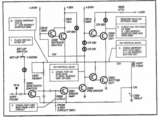
Fig. 4. Vertical amplifier circuit with check point call-outs.
HORIZONTAL SWEEP OUTPUT CIRCUIT (SOLID-STATE) RCA CTC 99/101 CHASSIS
This RCA CTC 99/101 chassis utilizes a conventional transistor sweep output system. All chassis operating voltages are derived from the horizontal output stage. For this reason, a problem in the horizontal output stage will cause other chassis functions to be inoperable.
Note that the horizontal output transistor may fail due to over-stress caused by a fault in some other chassis component. If a horizontal output transistor is replaced, you should perform the following service checks to prevent destroying the replacement transistor in the process of locating a defective component.
Some Symptoms
• Dead set
• Shutdown occurs
Troubleshooting Procedures
Caution: Use isolation transformer and unplug AC line cord for all static checks.
Refer to simplified circuit in Fig. 5 along with the service procedures indicated in the numbered blocks.
Defeat the regulator circuit by shorting across SCR 100. This can be accomplished by jumping between SCR 100 heatsink and TP 12 which are not shown in this circuit. Apply a reduced AC voltage through a variable transformer to supply a B+ voltage of about 40 volts. Apply +23 volts to the cathode of CR422 to operate the horizontal oscillator. Refer to Fig. 3.
Operating the horizontal output stage at near +40 volts allows troubleshooting of the stage while reducing the possibility of blowing out the horizontal output transistor or associated components.
NOTE: The horizontal output heatsink is not a HOT ground. Use the negative terminal on can of C106 (B+ filter capacitor) for a HOT ground.
Check the horizontal output base waveform at test point OB. If waveform is not present, suspect the horizontal oscillator driver transistor, Q407 or driver transformer, 1101.
Check the horizontal output transistor collector waveform at test OC. This waveform can be very useful for problem diagnosis. If the waveform shown in step 3 of Fig. 5 is present and correct, increase the variac output to supply approximately +123 volt DC. Now check the secondary B+ supplies to be certain if they are not excessive. If the B+ voltages are all normal then the sweep circuit is operating properly.
If the collector waveform of the horizontal output transistor is close to that shown in step 4 of Fig. 5, suspect shorted secondary B+ diodes or a defective sweep transformer. To further check for a sweep transformer short, disconnect the two secondary B+ diodes, + 210 volt and +23 volt supply. ff the waveform is still as shown in step 4, the horizontal output transistor is probably bad.
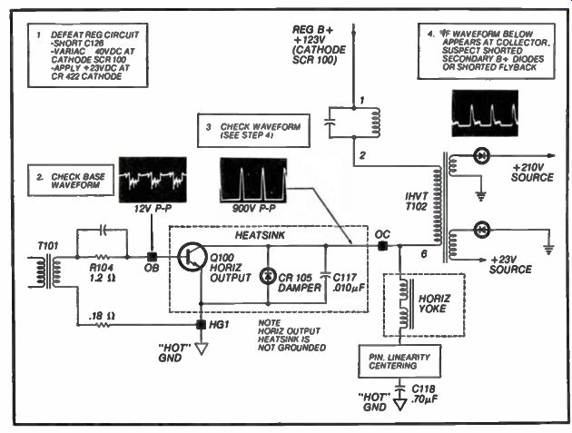
Fig. 5. Horizontal sweep output with scope waveforms.
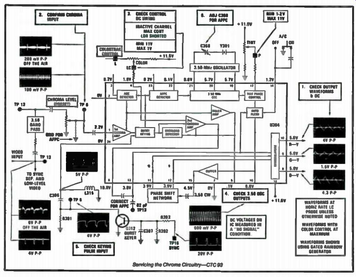
Fig. 6. Chroma circuit with check points and waveforms.
CHROMA CIRCUITRY (IC CHIP) RCA CTC93 CHASSIS
This sophisticated RCA U304 chroma IC contains an ACC detector, AFPC detector, chroma amps., burst keyer, color killer, 3.58 MHz oscillator, buffers and demodulators. Refer to the block diagram in Fig. 6 for this chroma chip circuit, and the scope waveforms that should be found for normal set operation of color reception.
Color Symptoms
• Weak color.
• Improper color.
• Improper tint.
Circuit Diagnosis
The symptoms listed above are almost always associated with a fault in the chroma circuitry. However, color faults can be caused by troubles in the video IF circuits. Should you find no chroma input signal to the IF circuits, then a faulty "front end" or tuner would be indicated. The tuner can be checked by inserting a video signal containing 3.58 MHz information to test point 6 located on the main chassis board. Signal amplitudes of . .1 volt to .8 volt p-p should produce good color on the screen.
Note that the color bars may or may not be in sync. Use a color-bar test generator for this check. Since all color processing operations are performed by the integrated circuit, most of the color problems will be caused by the U304 chip.
Service Checks and Tips
Use an isolation transformer and unplug AC line cord during all static test procedures.
NOTE: All waveforms are taken with the color control at maximum and a keyed color-bar rainbow input test signal. Allow the set and any test instruments to warm-up 5 or 10 minutes before any tests or measurements are performed.
Points of Service
Check at pins of the chip with a scope for any missing or incorrect waveforms. Referring to Fig. 6, check and see if you have the correct DC voltages at all pins of the U304 IC as indicated.
With the scope, confirm that you have the correct chroma input signal at TP 6.
Check the chroma level (preset) for proper DC swing, 1 to 11 volts with a maximum to minimum color level.
Check for 3.58 MHz oscillator sinewave output signals at pins 11 and 12 of the IC. Again, with the scope, check the keying pulse input. If the pulse is missing, there will be no color. This should be checked at the input of Q312 (station sync), and directly at pin 24 of the IC. Some AFPC Adjustment Tips Adjust the 3.58 MHz oscillator trimmer capacitor C368 by using the following procedure.
• With color-bar generator, feed signal to the RF input.
• Ground TP 6. Make this ground connection as short as possible.
• Connect TP 13 (video output from IF) to C377 (pin 13 of chroma IC) via an 82 pF capacitor.
• Adjust C368 to zero beat the color-bar pattern. Use a nonmetallic screwdriver.
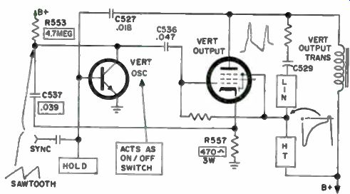

Fig. 7. Vertical sweep circuit with operational guide.
HYBRID VERTICAL SWEEP CIRCUIT
This hybrid vertical sweep circuit will be found in the RCA CTC-36 and other chassis. Referring to Fig. 7 we see that this circuit is comprised of a transistor oscillator stage and a pentode output stage. The pentode is a special type, having a diode plate which utilizes the common cathode of the pentode. This diode, in conjunction with a resistance capacitance network coupled as a feedback between the output and the input electrodes of the pentode, develops a feedback voltage for addition to the sawtooth waveform for vertical linearity and size control. Another feedback path, to sustain oscillation, is from the output stage to the base circuit of the transistor oscillator. The base circuit is also the input where the vertical sync pulses are injected. The vertical control circuitry (V hold control) is designed to adjust the triggering waveform component to the base of the oscillator. The height and linearity circuits operate in conjunction with the pentode stage.
The transistor oscillator stage acts as an on-off switch. A resistance capacitance sawtooth generator circuit (R553, C537) coupled to the grid of the output stage is subjected to alternate charging from the B+ supply and discharging through the transistor in an operating cycle recurring at the vertical sweep rate. Thus, the charging path for C537 is completed through the cathode resistor of the output tube. The oscillator transistor conducts during retrace time to provide a discharge path for the sawtooth capacitor. The sawtooth voltage developed across (C537) is coupled via (C536) to the control grid of the output stage. This grid voltage waveform, which is substantially linear, causes plate current to flow in the output stage. The plate current variation of the output stage is coupled to the deflection yoke by means of a vertical output transformer.
During the trace portion of each deflection cycle plate current increases causing plate voltage to decrease in a substantially linear manner. At the end of vertical trace time, a positive polarity synchronizing pulse is fed via a capacitor to the base of the oscillator transistor, driving the transistor into conduction. As the transistor conducts, the voltage across C537 decreases rapidly, driving the control grid of the output stage negative.
When the output stage is driven into cutoff, the plate voltage waveform increases rapidly as a result of the energy stored in the deflection yoke windings. The developed positive pulse, coupled through C527 to the base of the oscillator keeps the transistor in a conductive state.
Near the end of vertical retrace, as the positive waveform decreases, the oscillator transistor is turned off. Capacitor C537 then starts to recharge in order to begin the next deflection cycle.
During retrace time the capacitor (C529) in the linearity circuit is charged through the conduction of the internal diode. The discharging of this capacitor through the linearity and height control circuits, during field scan, provides the feedback waveform for linearity. The linearity control setting determines the amount of charge that C529 receives during retrace. Thus, the proper waveform for linearity can be attained.
Adjustment of the height control, however, primarily determines the average DC of the waveform, and in so doing provides the bias control for proper picture height setting.
The detailed circuit shown in Fig. 8 of the vertical oscillator and output stage, will now be used to point out several other features. The oscillator is provided with an additional triggering waveform component derived from one of the transformer secondary windings. The waveform is coupled to the base circuit of the oscillator via R414, the vertical hold control, and R546. DC base bias is provided by R419 coupled from the B+ supply to the junction of the hold control and R414.
A diode (CR 502) is coupled across the sawtooth forming capacitor C537. The purpose of this diode is to prevent an instability condition, as the C537 would otherwise charge to the cathode voltage potential during retrace; any disturbance in the output tube could then be regenerative and cause some picture jitter. With CR502 in the circuit, the voltage across C537 at the start of each cycle is kept constant (due to forward drop in diode) and independent of what the cathode voltage was in the preceding cycle. Thus, by assuring that at the start of every cycle the grid drive on the tube always starts at the same point (for a given setting of the controls) the vertical jitter will be prevented.
A VDR (RV 602) is located in the height control circuit to maintain a constant reference voltage to provide height tracking with line voltage variations.
The normal-service-raster (set-up) switch grounds the grid circuit of the output tube through a 1.8K resistor when in the service position, to collapse vertical sweep for making color temperature (grey scale tracking)
adjustments. The function of the 1.8K resistor is to provide protection for the diode and transistor from picture tube arcs.
PLATE-COUPLED VERTICAL SWEEP CIRCUIT (TUBE TYPE)
The vertical sweep oscillator turns off and on (be it tube-type or solid-state) approximately 60 times each and every second. A pulse from the sync separator stage is used to turn the vertical oscillator on at the proper time.
You can consider the height control circuit as the components between the vertical output stage and the vertical oscillator stage that control turn-on time. The vertical linearity circuit is used to connect the sweep output circuit with the vertical oscillator circuit to control this length of time. Hence, it controls the time on and off of the sweep output circuit or the actual length of time to stay turned on.
As we now see, the vertical sweep system can be broken into two basic stages. The vertical oscillator stage whose on/off timing is controlled by a sync pulse from the sync separator stage. The vertical output (amplifier) stage that is turned on and off at a 60 Hz rate by the vertical oscillator and is controlled via the height and linearity circuits.
Again, the height and linearity circuits control how long the output circuit stays turned on and off. See Fig. 9.
So, the vertical sync pulse holds the vertical oscillator to the correct speed while the vertical output stage then develops the proper raster scan size for the picture tube.
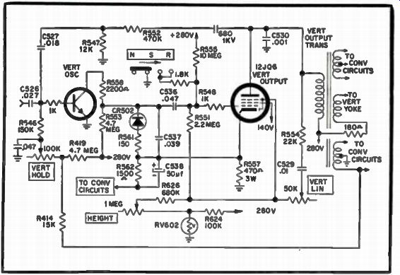
Fig. 8. Vertical oscillator and output circuit.
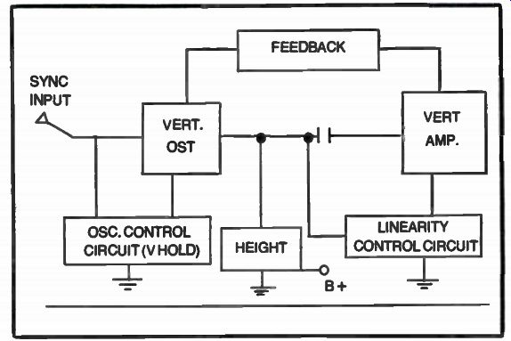
Fig. 9. Block diagram of plate-coupled vertical sweep system.
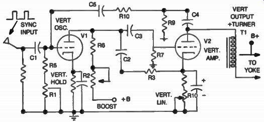
Fig. 10. Simplified diagram of a multivibrator.
With just these two blocks the vertical circuit seems quite simple.
However, things do become more complex when you consider the feedback loop from the output stage that may be used for vertical height, linearity or vertical sync pulses.
PLATE-COUPLED MULTIVIBRATOR (TWO TUBE TYPE VERTICAL OSCILLATOR AND AMPLIFIER)
The vertical sweep system shown in Fig. 10 is a plate-coupled multivibrator consisting of V1 and V2. For the oscillator portion, V2 (amplifier) is the normally off tube. Coupling from the plate of V1 to control grid of V2 is via C3 and R7. The feedback from the plate of V2 to the control grid of V1 consists of C4, R9, R10 and C5. This network is also a shaping circuit and ensures that the voltage fed back has correct amplitude and waveform to sustain oscillation.
C1, R1 and R5 control the main frequency, determining the RC time constant of the circuit. Check these components if you have oscillator drift, which of course causes vertical picture roll. The vertical hold control R1 is located in the grid of V1, the tube that is normally off. R2 is the height control while C2 and R3 constitute the shaping network across which the output trapezoidal waveform is taken.
The output from V1 is now coupled via C3 to V2 the vertical amplifier stage. Next, the vertical output transformer couples the trapezoidal waveform to the deflection yoke. Note that a positive sync pulse is fed to the control grid of V1, the normally off tube to synchronize the oscillator.
The output amplifier found in the vertical sweep stage of a tube type TV receiver is a power amplifier. A high current carrying triode or power pentode is usually used. A power amplifier is required because the deflection yoke winding is a current driven coil. Deflection is accomplished by the changing magnetic field around the yoke, which occurs because of a changing current through the yoke windings.
The voltage waveform which appears in the control grid of the vertical amplifier, V2, has been shaped to cause linear deflection. With a scope you will see the familiar trapezoid waveform (see Fig. 11) which will appear in the output of the vertical amplifier.
Brief Vertical Sweep Circuit Review
A typical vertical sweep circuit (see Fig. 12) used in many Zenith sets features an oscillator and amplifier, with the amplifier acting as part of the oscillator. The vertical oscillator triode (V5A), discharges and couples a strong pulse into the vertical output grid, (V5B) which is a class "A" amplifier, via the set-up switch and C76. This in turn couples a higher pulse to the output transformer and yoke for deflection. For the feedback action, a portion of the output pulse is looped back from the plate, pin 4, via .01 e (C71), a 47K resistor, then on to .0039 uF (C73) and a 100 K resistor to the oscillator grid pin 10. This triggers the next discharge pulse. The vertical sync pulse is coupled into the cathode, pin 11, at a point above the X5 diode.
Some Troubleshooting Comments
When a multivibrator stage is faulty, it is usually tough to troubleshoot the circuit while in operation unless a signal is injected into the circuit. The injected signal is then followed through the circuit (with a scope) to locate the point where the signal path is broken. The test signal can be fed in at the sync input point by using the TV stations sync pulse.
Another simple way to check the vertical sweep section is to couple an AC signal from the sets tube filament transformer winding with a capacitor over to the sync input point. This 60 Hz AC signal is then traced with a scope through the vertical oscillator stage (now acting as an amplifier) on through the coupling network and the second oscillator stage (vertical output amplifier) and then back via the signal path (feedback circuit) to the vertical oscillator section. Of course, the shapes of the waveforms will be modified by the various shaping networks. The signal amplitude and its waveform are your clues to a defect, since you will be looking for a breakdown in the signal path or a low signal amplitude which may be preventing normal oscillation.
Vertical Sweep Trouble Symptoms
The following is a list of trouble symptoms that indicate a problem in the vertical sweep system:
• Complete loss of vertical deflection.
• Partial loss of vertical deflection (may have foldover).
• Excessive vertical deflection (picture stretched out).
• Intermittent sweep.
• Vertical picture roll (may want to roll after set warm-up).
• Vertical picture jump and/or jitter (usually caused by a sync trouble).
• Intermittent or pulsating vertical sweep or roll (the bouncing ball affect).
• Vertical picture nonlinearity.

Fig. 11. Trapezoidal waveform for the vertical sweep.
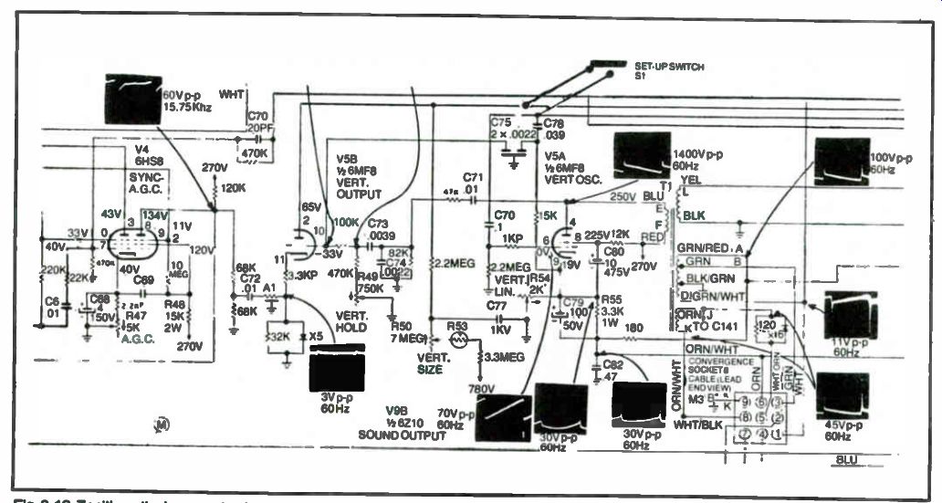
Fig. 12. Zenith vertical sweep circuit.
Vertical Circuit Quick Checks
Let's now look at some ways to make some vertical circuit checks to quickly isolate the faulty component. For these following circuit checks and trouble tips we will be referring to the vertical sweep circuit used in a Zenith 15Y6C15 color chassis. See Fig. 12.
We will begin these points of service checks with a set that has complete loss of its vertical sweep.
The first step is to open the feedback circuit at the junction of the 47K resistor and .0039 / if' capacitor (C73), which should now produce a horizontal line across the screen due to complete vertical collapse. Should complete vertical collapse not occur, the vertical output stage is oscillating itself in the absence of a vertical drive signal. Check (C82) .47 uf, (C79) 1001.uF, the exact value of 15K resistor from cathode pin 9 and the vertical linearity control (R54), as a fault with one of these components may be causing the oscillation.
Now connect one end of a .1 uf, 600 volt capacitor to the sets 6.3 volt AC filament terminal leads. Use the other end of the capacitor, through a clip lead, as a 60 Hz drive signal, to check sweep circuitry performance.
With this set-up, touch the test lead to the vertical output plate, pin 4 of V5B. A one-shot negative kick will appear on the screen as the .1 uF test capacitor charges up. The vertical sweep on the sets screen should now increase to several scan lines, indicating that the output transformer circuits and the deflection yoke are good.
Should no deflection occur suspect the following components.
• Vertical output transformer or yoke could be faulty or open.
• Plate load resistor for V5A. Check for 250 volts B+ at pin 4.
• Some sets have a vertical centering pot. If open, this will cause loss of deflection.
• Check the 12 K ohm screen grid resistor and capacitor C80.
• Vertical linearity control R54 may be open.
• Also faults in the pincushion circuit and on the convergence board will cause loss (sometimes partial) of the vertical sweep.
Partial Vertical Deflection Checks
Some shorted turns of the vertical output transformer can cause partial loss of vertical deflection. A more common trouble is an open capacitor, C73, from cathode to ground of the V5A tube. For a quick check just bridge a 100 µF, 450 VDC capacitor across C73. Make sure you connect the test capacitor with the proper polarity. Note that on some brands of sets this capacitor may be located on the convergence board.
Also, R55, the 3.3 K ohm cathode resistor may have increased in value.
Just bridge another resistor across to see if you now have full deflection sweep. The vertical sweep output cathode circuit is also returned through some of the controls on the convergence board. So, check these, they may be open or you may find a crack in the PC board.
If the sweep circuit has checked out OK up to this point, then inject the test signal into the vertical output tubes control grid, pin 6. Since this stage is a class A amplifier, the scan on the picture tube should display about 3 inches of vertical sweep (sinewave, not sawtooth) which will indicate that the output stage is good.
With the 60 Hz test signal fed to the vertical oscillator plate, pin 2 of V5 A, an identical deflection to that observed on the vertical output grid, indicates that the set-up switch and the (C76) coupling capacitor are good.
If no deflection is observed then suspect a faulty (usually open) coupling capacitor between plate of oscillator and control grid of the vertical output tube. Also suspect any capacitors tied to the coupling network (such as C75) as they could be shorted or have some leakage and will bleed-off the signal before it reaches the output stage grid. Also, look for open or increased-in value resistors in this network. Also, a faulty set-up switch S1, will cause a loss of vertical deflection or erratic vertical sweep action in this circuit. The switch may have developed leakage to ground or the contacts may be dirty and this will cause the vertical sweep deflection to be intermittent.
Oscillator Grid Injection Checks
Before placing the test capacitor on the vertical oscillator grid, pin 10, connect the set for normal viewing by tuning in an active TV channel. Now clipping the test capacitor to pin 10, should create a full picture scan, indicating the vertical circuit is functioning properly, except for the disconnected feed-back loop. Picture will tend to roll around vertically (see Fig. 13) since the triggering (sync-lock) is at the 60 Hz AC line frequency rate.
Connecting the test capacitor to the loose end of the .0039 uF capacitor (C73) in the feed-back circuit should produce a vertical picture sweep, but at a reduced amplitude. You can also hold the (C73) capacitor between your fingers and obtain some vertical sweep, amplitude being dependent upon the amount of random 60 Hz AC picked up via your body capacitance.
With the feedback circuit now connected, you should have normal vertical sweep. If not, then some component in the feedback loop (between plate of output stage and control grid of oscillator) is open, or a by-pass capacitor to ground, or a capacitor to another portion of the vertical circuit is shorted. The prime suspects would be C73, C71, C74, and the 100K and 47K resistors.
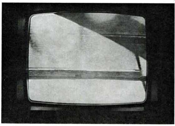
Fig. 13. Picture roll caused by 60 Hz AC in the oscillator circuit.
In order to keep oscillating, the vertical circuit relies on the 60 Hz pulse that comes from the plate of the vertical output stage, through the feedback loop, and to the control grid of the oscillator stage. Without this pulse, the vertical oscillator stage would actually go into saturation, thus shutting down the whole vertical sweep operation.
In summation, when an oscillator (multivibrator) is faulty, it can be tough to troubleshoot when it is in operation unless a test signal is injected into the circuit. This test signal can then be followed with the scope in order to pinpoint the place of signal path interruption. If the 'TV station sync pulse cannot be used, then a test capacitor is an easy way to couple a 60 Hz AC signal from the sets tube filaments to the vertical circuits sync input point. The test signal is then traced with a scope through the oscillator stage (now acting as an amplifier) through the coupling networks and onto the vertical output stage and then through the feedback circuit to the first stage again.
Vertical Oscillator Frequency Checks
Loss of vertical frequency control (no picture lock or vertical roll) may be caused by loss or attenuation of the vertical sync pulses, or to value changes in the frequency determining components in the oscillator stage.
You can easily determine if the oscillator is at fault by varying the vertical hold control. ff the picture can be rolled up and down, it is almost a sure bet that the oscillator is operating properly and the trouble is caused by loss of, or improper sync pulses. You should now suspect a fault in the sync circuits or in other circuits that supply information to the sync stages.
If rotation of the vertical hold control will not roll the picture in both directions, then look for trouble in the oscillator circuit. Probably the quickest way to locate the fault is to check-out or sub-in each component in the oscillator circuit as there are only a few. Prime suspects would be the tube itself V5, or C73, C74, 100K resistor, 470K resistor, C75 special dual-capacitor and the vertical hold control, R49. The fast vertical roll in Fig. 14 was caused by a leaky C73, .0039 ,ÁF capacitor.
If diode X5 in cathode of V5A becomes shorted there will be no vertical picture lock-in. This fault causes the sync pulses to be shunted to ground. An open X5 diode and/or value change of the 32K resistor will cause no vertical sweep or a reduced deflection. A pulsating vertical sweep, sometimes referred to as the bouncing ball affect, is caused by a faulty Al integrator RC network.
Vertical picture jitter and jump is usually caused by components that are intermittently going bad. Also, a hum bar creeping up the screen will make the picture jitter. A light shade drifting bar is usually due to a signal path trouble, while a black bar is a fault in the DC power supply, such as an open filter capacitor. And do not overlook leakage between multi-section filter capacitors.
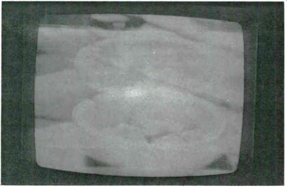
Fig. 14. Leaky capacitor causes fast vertical roll.
Vertical Picture Foldover and Stretch In most cases, the reason for picture foldover, is improper bias on the output amplifier tube, which results in overloading, or an improper sweep-voltage waveform fed to the output tube.
If the trouble is caused by wrong bias, a scope check at the grid, pin 6 of V5B, will probably show a clipped waveform at this point. Our job then, is to find the reason for this clipping.
A leaky coupling capacitor C76, a shorted cathode by-pass C79, or a shorted vertical linearity control R54, would up-set the bias on the vertical output stage and cause foldover.
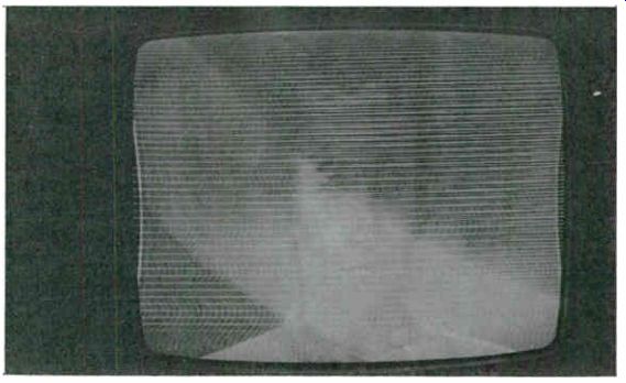
Fig. 15. Faulty VDR causes picture to stretch-out.
A voltage check at the control grid should give you a clue to the problem. Thus, a positive voltage metered at the control grid of V5B, would indicate a leaky capacitor C76. And of course, a zero cathode voltage reading would point to a short in the cathode circuit.
A long stretched out picture is generally caused by too much vertical drive signal from the vertical oscillator. The stretched out picture shown in Fig. 15 was caused by a faulty R54 VDR in the height control circuit.
The clue, in this case, was way too high plate voltage, pin 2 of V5A, on the vertical oscillator stage.
Nonlinearity of Vertical Sweep
Improper operation of the vertical amplifier, which causes a non linear picture as shown in Fig. 16, is usually caused by improper grid bias or low voltages on the plate or screen grid. A defective linearity control may cause the picture to be non-linear. And a leaky coupling capacitor C71 can also cause non-linearity without foldover. In both cases the amplifier is affected. A waveform, voltage and resistance analysis of the V5B amplifier should point you in the right direction. Leakage in C80, an increase in value of the 12K resistor at the screen grid, pin 8, or a defective Ti vertical output transformer can cause a non-linear sweep.
And of course, open filters in the B+ voltage supply can cause the same symptoms. You may or may not see a hum bar across the screen.
Non-linearity may also be caused by a non-linear sweep waveform coming from the oscillator stage. Thus, if the values of C77 or the 2.2 meg resistor have changed, the waveform from the oscillator could be distorted. Waveform, voltage, resistance checks or parts substitution in the oscillator stage should correct the trouble.
THE ZENITH SYNC/AGC PROCESSOR CHIP 221-45
Because of tremendous TV signal variations and interference found in actual reception, some complex IC circuitry has been designed in order to produce a stable picture. This, of course, is referred to as the sync./AGC circuitry. In the Zenith sets this sophisticated chip is known as the sync/AGC processor. It is found in the 9-87 plug-in module.
Briefly, the AGC circuit senses the amount of signal received by the TV set after it has been amplified by the tuner and IF stages. A DC control voltage developed by the signal strength is then fed back to the tuner and IF amplifiers to adjust for proper output signals. In order to have a good signal-to-noise ratio, the gain of the IF amplifiers is reduced before the tuner gain is reduced.
To help you see the total picture for this processor chip operation, refer to the block diagram in Fig. 17 of the complete sync/AGC system which is contained on the 9-87 plug-in module.
The video information that the TV station transmitter broadcasts is, of course, amplitude modulated. This AM video signal will vary according to picture information and cannot be used as a reference to produce the AGC voltage. Because the horizontal sync pulse does not vary, except for changes in signal strength, it is compared to an internal reference to develop the AGC correction voltage.
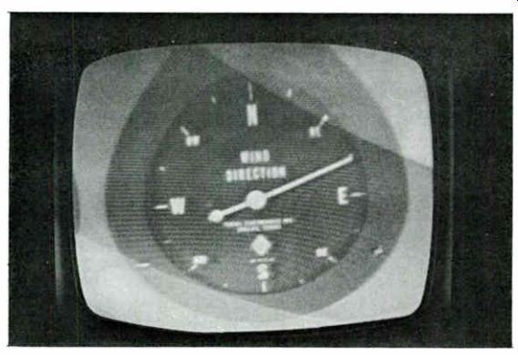
Fig. 16. Nonlinear vertical sweep.
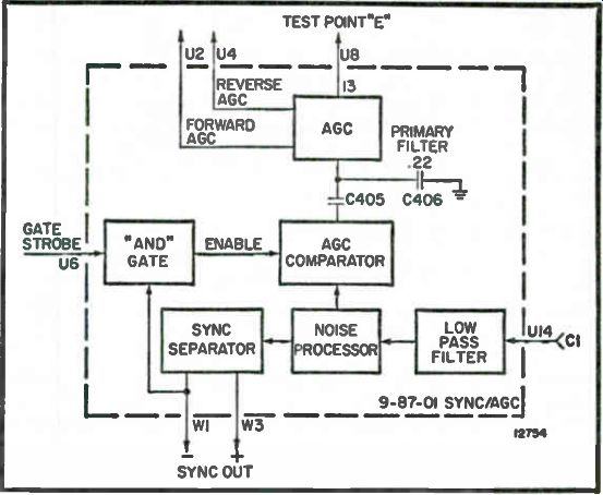
Fig. 17. Functional block diagram of the 9-87 module.
The AGC circuitry uses the horizontal sync pulses which are removed from the composite video signal by the sync separator circuit. They are then processed through a dual-time constant network to produce both horizontal and vertical sync pulses that are used to lock-in the vertical and horizontal oscillators. The complete video signal enters the processor chip and the sync separation function is performed from within.
Now we will take a close look at the Zenith processor IC, how to troubleshoot around it and its associated components plus, review some actual case history problems.
Video Processor Circuitry Operation (Zenith 9-87 Module)
The heart of the 9-87 plug-in module is the 221-45 video processor chip. Two signals are fed into the IC401 chip. One is the composite signal from the IF module and the other is the gating pulse from the horizontal circuit. The IC processor uses these two inputs to develop AGC voltage and sync information as well as performing noise gating and sync-limiting.
As we look at the various processor operations refer to the 9-87 module circuits in Fig. 18A and associated waveform check points. The correct scope waveforms (input and output signals) will appear as shown in Figs. 18B through 18E when all receiver systems are functioning.
Negative going composite video at test point C1, goes via a high frequency filter network formed by choke coil L211 and capacitor C220 to pin U14 on the 9-87 module. The function of this filter network is to remove high frequency components on the composite video signal, which could in poor reception areas interfere with normal sync limiting action.
These filter components could be prime suspects should you encounter poor sync locking action and a replacement module does not solve the problem.
The composite video signal enters the IC at pin 8 via a 1K resistor.
The chip at this point performs the noise processor function. When noise pulses beyond sync tip level appear at pin 8, IC 401 cuts off the AGC and Sync functions for the duration of the noise pulse. Turning off the sync function prevents the noise pulses from tripping the vertical and horizontal oscillators.
Noise Protection and AGC Gate Circuit (221-45)
Within the sophisticated 221-45 chip, is an AGC comparator which is gated so that fast slew rates can be utilized with good noise immunity. You will note in Fig. 19, the noise protection block diagram, that two gates are used. In order for the AGC filter to be charged or discharged, two inputs to the comparator must be present. As with other discrete AGC systems, the keying pulse must be present but additionally, the negative going separated sync pulse from the video signal must be present.
Coincidence of the two pulses will result in AGC action if the detected signal level changes. If, however, the sweep oscillator is out of step, no AGC action can occur until the keying pulse coincides with the signal sync pulse. Thus, no sampling or wrong sampling is made during scan time.
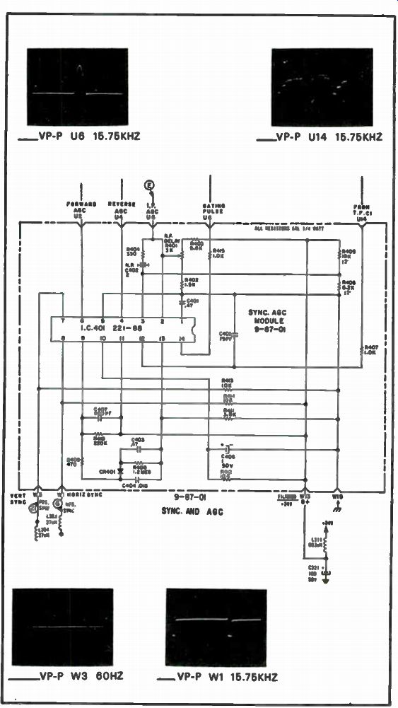
Fig. 18A. The 9-87 module circuit shown with its key waveforms.
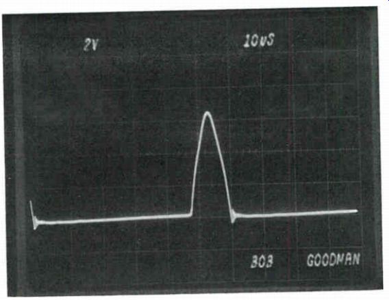
Fig. 18B. Horizontal keying pulse.
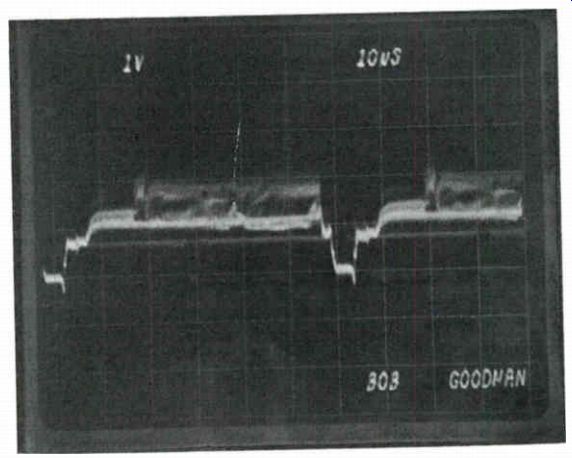
Fig. 18C. Composite video signal.
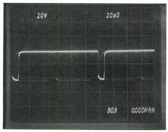
Fig. 18D. Horizontal sync pulses.
AND Gate Note
As Fig. 19 indicates there is a NOT input to the AND AGC gate in the noise protection circuit. Note the NOT circle at one of the gate inputs.
Remember that the NOT symbol indicates logic inversion. Just a note in passing, that you will now start finding these hybrid NOT-input gates in some of the newer generation VCR logic system circuits.
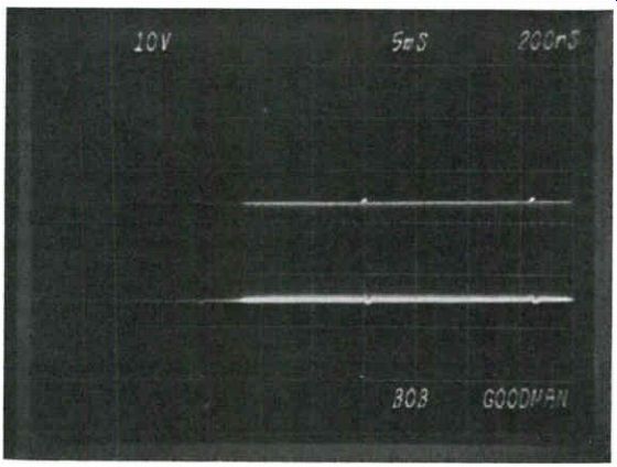
Fig. 18E. Vertical sync information.
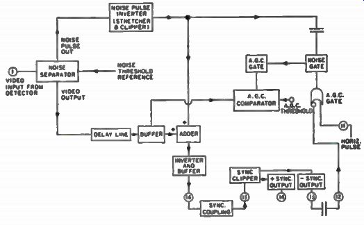
Fig. 19. Block diagram of the noise protection circuit
As the noise cancelled video signal leaves the IC at pin 5 it enters a dual time constant network of C403, C404 and diode CR401. This network provides the sync limiting stage with immunity to aircraft signal flutter.
After passing through the dual time constant network, the noise cancelled video signal enters IC401 at pin 4 and the sync limiting function is performed. Note sync separation location in Fig. 19. Internally, IC401 separates the video information from the sync and amplifies only these pulses. A positive going sync pulse appears at pin 3 of the IC and is the vertical sync. At pin 2 a negative going pulse is used to sync in the horizontal sweep oscillator.
The negative-going sync information at pin 2 is returned to pin 1 thru R404 and C402. The sync pulse is coupled to a gating circuit within the chip. Also, a positive-going horizontal gating pulse is coupled from the horizontal circuit thru R401 to pin 16 of the IC. Both the negative-going sync pulse and gating pulse is needed to key on the gating stage. AGC voltage can only be developed when sync is present which is during the retrace interval. This action occurs in Fig. 19 along the enable line from the AND gate to the AGC comparator stage.
Since AGC voltage can be developed only when sync is present, AGC voltage must be maintained during scan time. Capacitor C406 at pins 10 and 11 of the IC functions to hold this voltage. Also, if noise is present during the sync interval, the sync output will be cut off and C406 will hold the AGC voltage until the next gating pulse.
With no signal present, maximum IF AGC gain is set by the voltage divider comprised of R410 and R418. This divider sets close to +6 volts at pin 12, which in turn sets up a bias on a portion of IC401 that results in about +4.8 volts at pin 13. The +4.8 volts is added to the +DC voltage set by the AGC delay control. The resultant voltage is coupled thru R406 to the IF AGC output voltage at pin U8 of the module. On some sets this is flagged as test point E. When a strong TV station is tuned in, the internal circuitry of the IC increases the output voltage at pin 13 until maximum gain reduction occurs. This voltage is about +7 volts and is determined by the adjustment of the AGC delay control.
In addition to the IF AGC voltage, the IC produces two RF AGC voltages. The AGC voltage at pin 14 is for the field effect transistor (FET) RF stage in the VHF tuner. The AGC voltage present at pin 15 is used by the NPN bipolar transistor RF stage in the UHF tuner. These DC voltages on pin 14 and 15 will vary according to signal strength and type of tuners used in the set. You will not find an AGC level or gain control on these chassis that have the 221-45 IC. This is because of the IC processor design and tight component tolerances in the 9-87 module.
Troubleshooting the Processor Circuits
In this section we will not dwell on repairing the 9-87 module (a new or rebuilt one can easily be plugged in) but rather in checking the modules associated components, voltages and pulse waveforms. As we now look at these various troubleshooting tips and case history problems, refer back to the 9-87 module circuit in Fig. 18A along with the key scope waveform check points for reference information.
When you have a symptom that appears to be a sync/AGC problem, some circuit checks and observations must first be performed in order to get a handle on the situation. The first step is to determine if the problem is actually caused by a fault in the AGC and/or sync circuitry. Symptoms of weak video, loss of video, or distorted picture as well as loss of vertical and horizontal sync can be caused by faults in the tuner, IF stages, AGC/sync stages or power supply. The best way to start checking these sets to determine if the Sync/AGC stage is defective is to sub-in a good module for the one in question, and then adjust the AGC delay control. If this does not correct the problem, then go to the tuner and IF circuits for video problems and the vertical and horizontal circuits for sync problems.
Also, check for +24 DC at pin W13 and correct horizontal keying pulses at pin U6 of the 9-87 module. Should you not have a good substitute module, a variable DC power supply can be used to clamp the tuner and IF amplifier AGC voltages to normal operating levels. If a nearly normal picture cannot be restored, the defect may very well be in the tuner, IF stages or video circuits. At this point a tuner "subber" will help you pin-point the fault quickly.
Let's now look at some "real world" problems with this Sync/AGC module and IC. The Picture Symptom In this Zenith 19FC45 color chassis the picture would roll intermittently and tend to twist. On some channels several wide bands or streaks (see Fig. 20) would go across the screen horizontally. This picture trouble may or may not be of an intermittent nature. The top of the raster may also be of a lighter shade.
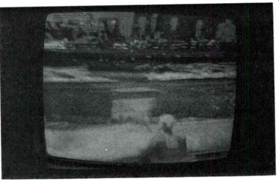
Fig. 20. Streaks caused by open filter capacitor at +24 volt input at
pin W13.
The Cause and Solution
The problem area, in this case, was found to be around the 9-87 Sync/AGC modules associated circuits. To pin down this problem several scope checks were made at various + 24 volt input module pins around the chassis. When the symptom occurred the scope indicated a lot of hash at pin W13, + 24 volt input terminal of the 9-87 module. The hash (horizontal pulses from HV sweep stage) was due to loss of filtering because of an open C321, 100 e by-pass filter capacitor. A replacement filter cleared up this picture problem.
For normal operation at all points where the + 24 regulated voltage enters the various modules the scope trace should be a smooth line even at high vertical scope amplifier gain. If you find hash or spikes on the scope look for open filter and by-pass capacitors or trouble in the 24 volt regulator circuits. Such as a faulty Zener diode or regulator transistor.
Also, make sure that the + 24 volt line measures 24 volts DC. A problem in the regulator circuit can lower this a few volts and cause a picture symptom that looks like sync or AGC trouble.
No Sound or Picture-Blank White Screen
This is a very common and simple problem but can be overlooked very easily. If module replacements do not restore operation check for + 24 volts at pin W13 of the 9-87 module. If no voltage is found, check for an open LX311 filter choke coil in the 24 volt line. This is a small 663 uH coil that may open up or at times will become intermittently open. Loss of voltage could also be caused by a shorted C321 filter by-pass capacitor.
Dual-Trace Scope Phase Comparison Check
A rare but tough to locate AGC problem can be caused by a phase shift in the horizontal keying pulse. An easy way to locate this type of trouble to use the dual-trace scope for simultaneously viewing the AGC keyer pulse (strobe) and horizontal sync pulse for correct timing. This will allow you to make an exact analysis of the two superimposed pulses. To check for this phase shift problem connect the synced in channel of the scope (usually the A channel) to pin 14 of the 9-87 module (video signal) and the B scope channel to pin U6, the horizontal keying pulse. Set scope at the horizontal sweep rate and adjust scope sync controls for a solid lock-in of the two pulses. The dual-trace scope photo in Fig. 21 illustrates the correct timing for a normally operating set. The horizontal sync pulse and strobe pulse must line up precisely.
A mis-timed keying pulse can be caused by some defect in the horizontal phase detector stage or any pulse coupling components. The dual-trace scope waveforms (Fig. 22) readily illustrate this out-of-time condition. Note that the keying pulse is actually in time with the 3.58 MHz color burst signal.
Another good point is to take note of the keying pulse width. If the pulse is too wide some video or 3.58 MHz color burst information may be sampled instead of the horizontal sync pulse level and this could cause the wrong AGC DC voltage to be developed. The symptoms would be picture overload, perhaps some bending or a washed out picture.
Another point of service is to check for proper filtering of the DC AGC control line. If a filter capacitor opens on this line the scope will show some hash. An open AGC line filter will cause various AGC picture problems such as overloading, bending and streaks across the screen.
Mysterious Picture Bending, Weaving and Rolling Symptoms
This intermittent picture problem (it appeared as an unstable sync or AGC fault) would occur on the local cable TV system in our area only on channels that were picked up via the satellite system such as Home Box Office, etc. This picture weaving symptom (see Fig. 23) would only occur in Zenith color sets using the sync/AGC modules with the 221-45 video processor chip. A new or rebuilt module has always corrected the problem. However, just replacement of the 221-45 chip will not always eliminate all unstable pictures on these cable channels.
Also, I have found some very fine and faint noise pulses that were detected on a very wide-band scope that appeared to be mixed with the horizontal sync pulses. Could this be some type of noise from outer space? If any reader has some ideas about this phenomenon, please let me know.
Perhaps these fine pulses were activating the noise protection circuit in the chip (due to one or more off-value components on the module and/or within the chip) and caused the IC's logic circuits to "gate-out" most of the sync pulses.
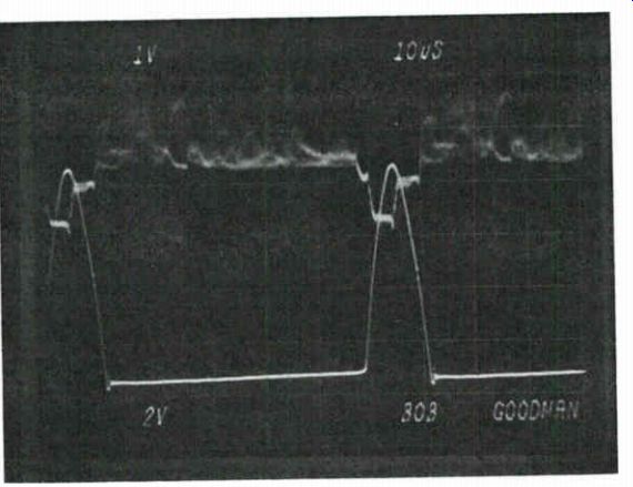
Fig. 21. Dual-trace scope indicates correct timing of the horizontal
keying pulse.
Some Module Checks and Tips
In about 90% of the cases a new 221-45 IC will solve any trouble that occurs with this module. As the circuit indicates, this module does not contain very many discrete components.
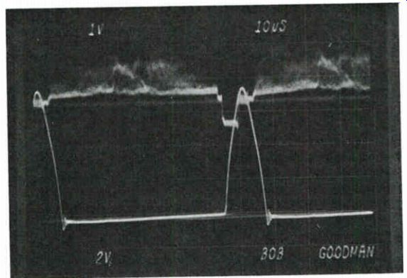
Fig. 22. Dual-trace scope showing mis-timed pulse.
While making a quick visual check of this module be on the alert for burnt or discolored resistors. Then use an ohmmeter to check for any off value resistors. You may then opt to check out the capacitors and the one diode.
For any intermittent problems on this module look for poor solder connections and cracks in the PC runs. Always clean and tighten all of the terminal pin spring contacts before the module is reinstalled. Also, check and clean pins on the main chassis where the module plugs in.
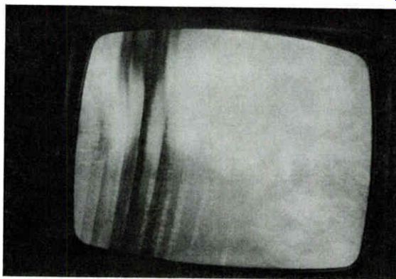
Fig. 23. Picture weave and roll symptoms found on local cable channels
received via satellite.
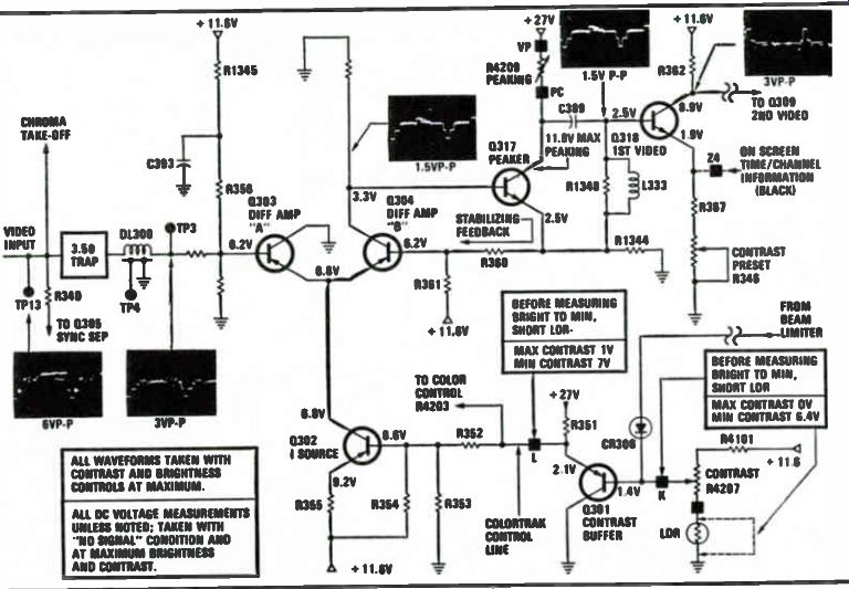
Fig. 24. Low-level video stage with check points.
VIDEO AMPLIFIER CIRCUIT (SOLID-STATE)
This low-level video circuit is found in the RCA CTC 93 and other similar RCA color TV chassis. One circuit that may be new to you is the differential amplifier.
Video Circuit Operation (Part A)
Composite video signals from the IF are fed to a common 3.58 MHz trap and then go via a delay line (DL 300) which feeds video to the base of differential transistor "A" (Q303). Refer to video circuit diagram, Fig. 24. Transistors Q303 and Q304 form a differential pair; while Q302 is the constant current source for the emitter-coupled pair. The more current supplied by Q302 to the differential pair Q303-Q304 will mean more contrast or gain.
The constant current source is controlled by the contrast control setting, LDR (Light Dependent Resistor) and action of the beam limiter via contrast buffer transistor Q301 (controls DC voltage supplied to the base of Q302 constant current source). At this point in the circuit, not only does the DC control voltage affect contrast, but also the color level.
After video signal contrast level has been set at collector of Q304, the signal is then coupled to the base of Q317 for video peaking. This stage provides stabilizing feedback voltage back to the base differential transistor Q304. The first video, Q318, provides for some additional gain and its emitter has a contrast preset control that is factory set.
Low-Level Video Circuit Operation (Part B)
The second video amplifier couples video (via C362) to the video buffer Q306. See video circuit in Fig. 25. With reference to waveform at emitter of Q306, sync tips have been removed and DC is restored at base of Q306 by action of the clamp stage Q307. Positive horizontal pulses coupled to the emitter of Q307 (via R369 and CR302) cause conduction of this stage, clamping capacitor C362 to a reference DC voltage. This reference voltage is set via the brightness control and goes to the base of Q307. If the horizontal pulses are missing, the clamp stage will not conduct.
Horizontal and vertical blanking pulses are elevated by action of the blanker stage, Q310. Both vertical and horizontal pulses are supplied to and amplified by Q310 and matrixed with the composite video signal on the base of Q309. In the waveform on the base of Q309, the elevation in blanking level at this point should be sufficient to drive CRT to cutoff during horizontal and vertical retrace. Diode CR303 carries the bias current due to R371 when blanker is off. Diode CR311 provides protection for blanker transistor Q310 to prevent overstress of the transistor when blanking pulses are applied.
When the clamp stage is operating properly, the video signal black level is referenced to the horizontal retrace blanking level and DC reference is effectively restored. The brightness control (R4202), as well as the beam limiter (Q311), can alter the base reference voltage of Q307, altering the re-established "black" level reference.
The video signal is then coupled from the emitter of Q306 via the service switch and respective drive controls in the R, G, and B matrix-amplifier stages.
Basically, beam current is caused to flow to the B+ supply through R378 (reference current is established) with a portion diverted to ground through the base emitter junction of beam limiter, Q311. Transistor Q311 is normally operated in a saturated state under normal brightness and contrast settings. As beam current increases and exceeds reference current, collector voltage of Q311 will increase and cause the brightness to decrease via CR305 and contrast to decrease via CR306. Thus, beam current is limited by a combination of reducing the video drive and brightness. A filter network removes both vertical and horizontal components found in the beam limiter current applied to Q311. Diode CR312 and R332 make up a beam limiter peak overload detector, allowing fast response to large beam current overloads. If too much beam current appears at Q311, CR307 acts as a protection device to protect Q311 from breaking down.
Video Servicing Procedures
Let's now look at some low-level video circuit troubles and techniques for troubleshooting them.
Video Trouble Symptoms and Diagnosis
• No or distorted video
• No or improper contrast control
• No or improper brightness control
• No control of contrast/brightness/color The low-level video processing circuitry has several direct coupled stages. Therefore, it is essential that the procedure described below be followed when troubleshooting any of the above symptoms.
Note that for sets equipped with FS Remote Scan Tuning Systems, there is essentially a built-in troubleshooting aid with the on-screen time/channel display. If no raster appears, but time and channel information appears on the screen, you can then assume that the low-level video stages signal path is OK from Q318 (1st video) to output of CRT. Troubleshooting Procedures Use isolation transformer and unplug AC line cord during all static checks. Refer to the block diagram (Fig. 26) for these procedures.
No or Distorted Video
Check set-up switch. An open set-up switch will cause a loss of raster or a very dim one as well as a loss of video.
With a scope confirm that you have a video input signal of about 6 volts P-P at TP 13. Now check the DC bias and circuit operating voltages, as well as waveforms at various video processing stages.
Check DC voltage on collector of Q311 beam limiter transistor. If DC voltage is between +18 and +27 volts, suspect open Q311 beam limiter transistor. An open transistor at this point makes both contrast and brightness controls inoperative. Screen will be totally black, even if chroma is turned to maximum.
Check blanker stage Q310, as improper operation can result in insufficient brightness.
No or Improper Contrast Control
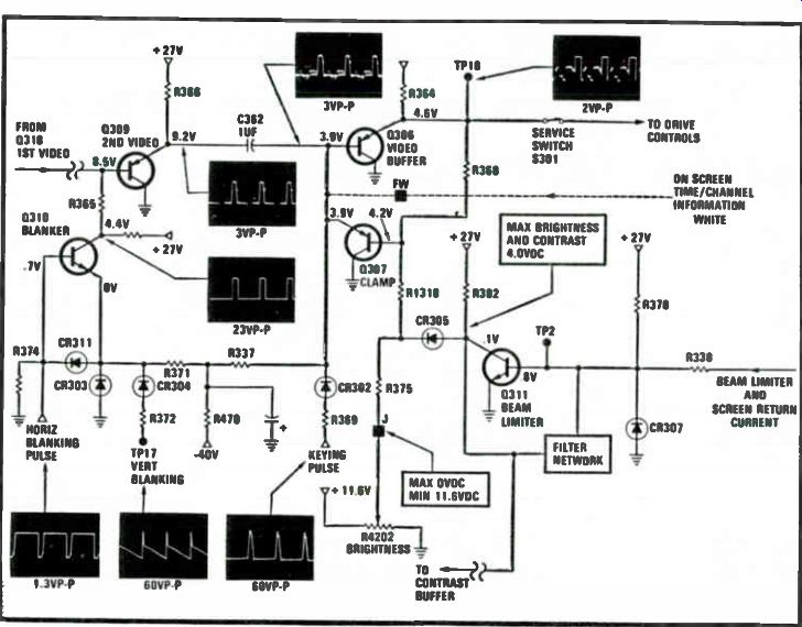
Fig. 25. Low-level video stage with scope waveforms.
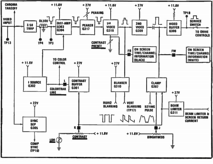
Fig. 26. Block diagram of low-level video stage.
Under this condition, screen will normally appear washed out and chroma control will have little effect. Check various DC voltages associated with the contrast control (test point K) and contrast buffer (Q301). Also check the color track control voltage (test point L), constant current source (Q302), and differential transistor pair Q303 and Q304. If DC voltage at test point (L) reads about +11 volts, assume contrast buffer Q301 may be open. Check diode CR306. If this diode is shorted the contrast control will not operate.
No or Improper Brightness Control
Check Q307 clamp action by scoping the base and collector of Q307 while varying the brightness control. As brightness control is decreased (ccw), video should go in the direction of black.
Confirm proper DC voltage range of brightness control (R4202) at test point (J). To isolate beam limiter stage from the brightness control and clamp stage, ground collector of Q311. If problem clears up, fault is most likely open beam limiter transistor Q311. If CR305 is shorted, this will cause the brightness control to be inoperative.
No Contrast/Brightness/Color Control
The very first check should be the collector voltage on Q311. As stated earlier, an open transistor in this circuit will cause all video and chroma stages to be inoperative. To remove any Q311 influence on video, contrast, and chroma, ground the collector of Q311.
POWER SUPPLY CIRCUIT (FULL-WAVE VOLTAGE DOUBLER, S-S DIODES)
This power supply circuit is used with TV sets that do not have a power transformer. Refer to Fig. 27 for this circuit as used in an RCA CTC 22 color chassis.
Circuit Operation
A 7 amp fuse in series with one side of the AC line is used for circuit protection. Surge protection is provided by a thermistor in series with the B+ rectifiers. The B+ circuit is protected by a special thermal reset circuit breaker. This circuit breaker, CB101, can be tripped by a combination of excessive current demanded of the low voltage power supply and/or excessive current via the horizontal output tube cathode circuit.
The CB101 circuit breaker has a resistive winding (about 1.3 Ohms) that completes the cathode ground return from the horizontal output tube.
If cathode current becomes excessive, the winding heats, causing the thermal bi-metal strip to expand unequally; the metal flexes, causing the breaker switch contacts to open, breaking the B+ line. The same action occurs if the B+ current increases due to a short circuit or overload.
Degaussing is initiated by the customer, using a spring loaded switch located on the back of the receiver.
The power supply drawing shown in Fig. 27 is actually a full-wave voltage doubler circuit. You will note that capacitor C106A functions differently than in a conventional power supply, as it does not act as a filtering capacitor. Operating with diode CR102, C106A charges to the peak value of the applied AC voltage. Using this DC charge as a reference, the other diode rectifier CR101 produces a DC voltage approximately equal to the peak-to-peak value of the AC line voltage supply. Hence, the DC voltage obtained is approximately two times (thus almost doubled) the RMS value of the input AC line voltage.
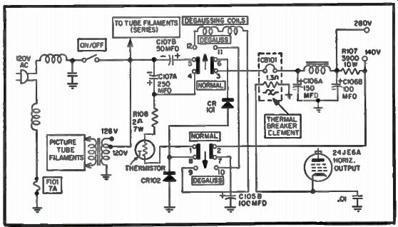
Fig. 27. Power supply and degauss circuit.
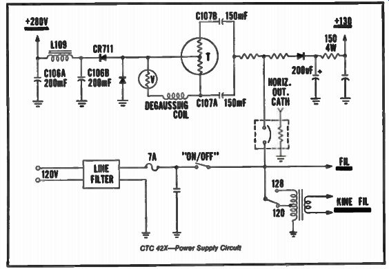
Fig. 28. Power supply circuit - full-wave doubler and half-wave rectifiers.
Power Supply for RCA CTC 42X Chassis
This power supply, used in the RCA CTC42X chassis shown in Fig. 28 has two separate power supply systems. The first is a full-wave doubler furnishing 280 volts B+ to the deflection, chroma, video output and audio output circuits. This power supply has provisions for automatic degaussing, using the circuit that was introduced in the RCA CTC22 chassis (tapped thermistor and split charging capacitor). The other power supply is a half-wave rectifier furnishing + 130 volts to the solid-state video IF, low-level video, sync/AGC circuits, and various tube screen grid voltages.
Power Supply Circuit Points of Service and Tips
The following is a list of various power supply circuit problems.
• No DC voltage
• Low DC voltage output (s)
• AC ripple that may cause bar to drift up or down the screen
• Picture will wave or weave
• Circuit breaker trips off
• Shorted diodes and filter capacitors
Refer to the circuit in Fig. 27 as we look at these various points of service and other information.
Complete loss of DC voltage could be due to a faulty on/off switch, CB101 circuit breaker, capacitors C107A and/or B, thermistor or degauss/normal switch.
Loss of the 140 Volt DC could be caused by an open R107 and/or shorted filter capacitor.
Low DC voltages will usually be caused by faulty filter capacitors (open or leaky) and diode rectifiers (open). All sides of the picture will be pulled in.
A circuit breaker that trips-out immediately is usually caused by a shorted diode CR102 or CR101.
A breaker that trips after about 30 seconds is usually caused by a problem in the horizontal output stage.
A set that operates an hour or more before the breaker trips is usually due to a faulty (weak) circuit breaker.
If the sides of the raster pull-in and weave, suspect filter capacitors C106A and/or C105B to be open. You may also see a bar that drifts through the picture.
If both sides of the raster pull in, suspect an open filter capacitor or a weak horizontal output tube. lithe right side pulls in, then look for troubles in the horizontal sweep stage.
When checking for a faulty diode rectifier use the lowest range of your ohmmeter and measure it in circuit as follows.
Diode Quick Checks
With the ohmmeter set to low range (X1) take a front to back ratio measurement (read in one direction, change polarity and make another reading). If the diode is shorted it will read dead-short for both polarities.
If the diode is open, the ohms value (resistance of in-circuit components) will read the same for either polarity check. Should the diode be good, you will now measure a lower resistance with one polarity than with the opposite polarity.
HORIZONTAL SWEEP-TRACE/RETRACE CIRCUIT (RCA TYPE)
The following horizontal sweep (trace/retrace) circuits will be found in RCA CTC72 and CTC81 color TV chassis and are similar to those found in many XL100 sets.
Oscillator Circuit Operation
The horizontal AFC and oscillator circuits of the CTC74 are contained in the MCH module. The AFC stages, along with the horizontal blocking oscillator and 33 volt Zener diode, are all located on this module.
The block diagram for the MCH-001 module is illustrated in Fig. 29. These stages include the Q1 phase splitter device, whose output is coupled to a pair of diodes for horizontal AFC, and thus control the horizontal blocking oscillator. Positive retrace pulses from the sweep transformer are first shaped by the sawtooth stage before being fed to the AFC stage. Operating B+ for the module stages is derived from a 33-volt Zener diode, initially fed from the 175 volt source via the dropping resistor.
A horizontal range control is connected in series with the customer horizontal hold control. Readjustment of the horizontal range control is seldom required, even when another module is installed.
The horizontal oscillator is a blocking type, connected as in many other XL100 RCA chassis. The output of the oscillator stage is used to initiate retrace, by "triggering" the retrace ITR into conduction.
Horizontal Trace/Retrace Circuit Operation
Figure 30 is a diagram of the trace and retrace circuits as used in the CTC 74 chassis and is similar to other XL-100 chassis.
Intrinsic thyristor rectifiers (ITR 401 and ITR 402) function in circuits similar to those using discrete SCR and diode pairs. ITR's were first used in the CTC 62 chassis, but these trace and retrace circuits are now more simplified.
Voltages in the CTC 74 chassis are developed directly from the power transformer. Thus, T402 no longer has secondary power windings for these voltages and the retrace circuit is more conventional in design than previous SCR systems.
The CTC 74 deflection circuits use a high-voltage transformer with an isolated primary. The top and bottom pin correction transformer is connected in parallel with the primary; the linearity network is in series with the yoke, and both are in shunt with the primary of the sweep transformer.
Operating power (175 volts) is derived from the main power supply circuit. This 175 volts (applied to the horizontal circuit) is obtained via a plug interlock connection and a relay in the power supply. The B+ path is completed by a jumper connection on the yoke plug. For this reason the yoke has to be connected before B+ is fed to the horizontal stages. In the CTC 74, ITR 401 functions as the trace SCR diode combination and ITR 402 as a dual retrace device. The gate signal from the horizontal oscillator to the gate of the retrace ITR is similar to other RCA chassis. Note that two .027 microfarad commutating capacitors are connected in parallel.
Key troubleshooting waveforms would be the trigger pulse at the gate of ITR 402, the commutating waveform at the anode of the device, and the pulse waveform viewed at the high side of the trace ITR. Also important is the gating waveform at the gate of trace device ITR 401. A keying pulse for the AGC circuitry is obtained via the 150 picofarad capacitor connected to the top side of the sweep transformer primary winding.
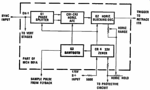
Fig. 29. Block diagram of horizontal IC stages.
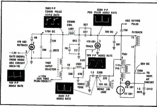
Fig. 30. RCA trace and retrace horizontal sweep circuits.
Because this chassis utilizes a self-regulating power input trans former, there is no need for a high voltage regulating circuit - either in the CTC 74 or CTC 81 chassis.
The simplified schematic in Fig. 31 shows the trace-retrace circuit for the CTC 81 chassis. The circuit is basically the same as in the CTC 74, however, provisions have been made for width and high voltage adjustments.
A width coil, L404, is connected in series with commutating coil L401; a jumper across L404 may or may not be found due to production tolerance. Width can be increased by opening the jumper and if the raster sweep is too wide, 1404 can be shorted.
The high-voltage adjustment switch, S401 in the primary circuit of T401, is not to be adjusted. This switch is usually sealed as shown in the diagram.