Figure 8-1 is a block diagram of the Bearcat 250 receiver. From a single antenna input, low/high VHF (32-50MHz - 146-174MHz) and UHF frequencies (420-512MHz) are coupled through track-tuned amplifier and mixer stages to a common I.F. (10.85MHz). A second oscillator at 10.4 MHz is used for mixing down to a 450kHz second I.F. which is limited and demodulated. The recovered audio is coupled to the audio amplifier and also filtered for activation of the noise-squelch circuit.
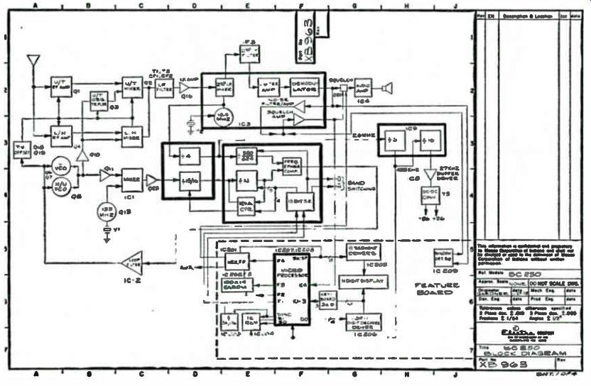
Fig. 8-1. Block diagram of BC 250 BEARCAT programmable scanner.
BEARCAT BC250 SCANNER CIRCUITS
The local oscillator signal is derived from a phase-locked-loop synthesizer. The VCO (voltage-controlled oscillator) frequency is divided down by a programmable counter which is preset from memory and compared to a reference frequency. Any frequency or phase difference produces a correction signal to change the VCO tuning voltage. This tuning voltage then forces the VCO to oscillate at the frequency required for the counter to produce an output that is in phase with the reference frequency. Thus, changing the modulus of the counter will change the frequency of the VCO. In order to increase the range of the counter, it is prescaled by 15 to 16 on all bands and the VCO is mixed with a 133 MHz oscillator on high band and VHF to achieve the higher frequencies required. For UHF, the VCO is then tripled to obtain its proper local oscillator frequency.
The frequency program is entered from a decimal keyboard into a microprocessor where it is multiplexed to drive the display and decoded to enter the proper binary code in memory to control the synthesizer.
VHF
An L or H band signal enters the receiver through the antenna. Coil Li attenuates frequencies that are below the low band, while diodes D1 and D2 limit the amplitude of very strong signals that would cause overload. The impedance looking into C1 from the antenna is relatively high, so the signal proceeds down to the parallel combination of C18 and L8. This circuit becomes parallel resonant in the U band and acts as a high impedance trap to keep UHF frequencies off the gate of Q4. L8 is a 2 turn coil which is practically a short circuit to the L & H band frequencies, so they pass directly to the gate of Q4. If a low band frequency is being received, the tank circuit for the gate consists of L9, LW, C21, and VVC4.
Transistor Q4 is a dual gate, N-channel MOSFET, which is the RF stage.
The tank circuit for the output consists of L11, L12, C25, and VVC5 for low band signals. The signal from Q4 is transferred through C28 to Q5, another dual gate MOSFET, which acts as the mixer stage. The local oscillator signal is supplied through C27 to the second gate of Q5. The oscillator frequency is 10.85MHz lower than the signal frequency, so the output frequency is 10.85MHz. The load on the drain of Q5 is tuned to that frequency.
The signal flow for a high band input from the antenna is the same as for the low band except diodes D3 and D4 are turned on by the band switching circuitry. This shorts out L10 and L12 respectively, causing the inductance in the tank circuits to be reduced to the lower values needed for operation at the higher frequencies.
UHF
A U band signal at the antenna is coupled through C2 to a tank circuit consisting of VVC1, C2, L2, and L3. It is tapped down to a lower impedance and then passed on through C3 to Q1, the RF amplifier. This is a grounded base stage and the output tank consists of VVC2, C5, L5, and L6. Once again the impedance is tapped down, and passed on to the base of the next stage, Q2, a bipolar transistor which is the mixer. The local oscillator signal is also supplied to the base of Q2 through capacitor C9.
The load of this stage is tuned to the 1st I.F. frequency (currently 10.85MHz). Q3 is the U/T Trippler.
V.C.O.
The Voltage Controlled Oscillator for high and UHF bands is Q8 with the frequency determined by L14, C32, C33, and VVC7. These components permit the control voltage on VVC7 through R31 to tune the oscillator through the required local oscillator frequency range (135-167 MHz) required for high and UHF bands.
In low band, the collector Q12 is high disabling Q8 which allows operation of Q6 and Q7 (LOW BAND VCO). The tank circuit consists of L13, C29, and VVC6 with feedback provided by C28. These provide the required LOW BAND oscillator range from the control voltage supplied through R24.
Track-Tuning
The Tuning Voltage versus Frequency Curves, shown in Fig. 8-2 produced by both VCO ranges, are used as the reference for track-tuning all R-F circuits.
The H/U/T VCO voltage curve is applied directly through R76 to VVCs 1, 2, and 3 to tune the U/T circuits to resonance for each frequency.
In high band, the voltage required to tune the RF circuits is more than the voltage produced by the H/U/T VCO. Therefore, Q18 is turned on in high band to provide a positive offset current through R71 and R11 to produce the required high band tracking curve as shown in Fig. 8-2.
For low band, the voltage required for tracking the RF circuits is less than the low band VCO voltage. Q19 is used to sink current through R75 to drop voltage across R76 to produce the L Band tracking curve shown in Fig. 8-2.
I.F. Section
The output of the low and high band mixer is fed into the primary of Ti, which steps the output down to a level that is comparable to the output level from the U band mixer. The signal, which is now at the 1st I.F. frequency (10.85MHz or 10.8MHz) goes through two crystal filters CF-1 and CF-2 to transformer 12. This filters out all frequencies except the I.F. and its modulation sidebands. From T2 the signal is coupled to Q16 which is just an untuned I.F. amplifier which increases the signal level that is fed into pin 16 of IC3.
Referring to Fig. 8-3, the I.F. signal at Pin 16 of IC3 (NB53101) is mixed down to the second I.F. The second oscillator is within IC2 and is controlled by the external crystal, Y1. This 10.4MHz oscillator is internally mixed with the 10.85MHz I.F. input to produce the 450kHz second I.F. at Pin 3. The second I.F. is coupled through CF3 (Ceramic 450kHz filter) to the I.F. amplifier input at Pin 5. The I.F. is then limited and demodulated with the recovered audio output at Pin 9. T3, R63 and C65 provide the phase shift to balance the demodulator.
Audio
The audio at Pin 9 of IC3 goes through the low-pass filter of R70 before coupled through C71 to the volume control R88. R82, C75 and R83, C76 form two additional pass circuits before the audio reaches the input of IC4 (NC66-301, TCA8305) which provides amplification to drive the speaker. The function of the external components is shown below.
• R-84 sets the closed loop gain of the amplifier.
• C-82 & R-85 reduces. saturation losses during positive half wave.
• C-79 sets upper cutoff frequency.
• C-81 couples audio to speaker and sets low cutoff frequency.
• C-80, R-86, & C-78 increases high frequency stability to prevent oscillation.
• C-84 & C-83 filters the ripple in power supply line.
Squelch The noise squelch system uses an operational amplifier (see Fig. 8-4) within IC3 as a bandpass amplifier. The resonant frequency (8. 5kHz), Q, and gain are determined by external components R67, R68, R69, C68, and C69. It is necessary to use this high frequency noise so normal audio frequencies do not activate the squelch system.
When no transmission is being received, the high frequency noise (8. 5kHz) is amplified by IC3. The noise is then coupled through C67 and detected by D13 to produce a negative voltage which is filtered by R81 and C74. This negative voltage is then applied through R135 to pin 12 of IC3 which overcomes the positive bias provided by the squelch control R78 through R217 and R218 to pins 1 and 7 respectively of IC209 which are both normally high (+8.4 volts). With the voltage at pin 12 below the turn on level (due to the negative voltage from the detected noise) pin 13 voltage will go high to permit the receiver to scan and pin 14 will be low, shutting off the audio at the volume control R31. When a signal is received, the resultant I.F. produces noise quieting through the system which reduces the 8. 5kHz noise amplified by IC-3, thereby reducing the negative voltage level from the detected noise. This reduced negative level permits the positive bias of R78, R217, and R218 to reach the turn-on level at pin 12 of IC3 which forces pin 13 to go low to stop scanning and shuts off the pin 14 output to enable the audio to reach IC1 for amplification.
Q17 inverts the squelch output at pin 13 of IC3 to provide the scan control to the microprocessor on the feature board. The collector of Q17 is also fed back to the squelch input (pin 12) through R66 to provide squelch hysteresis.
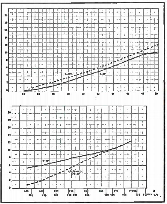
Fig. 8-2. Tuning chart curves.
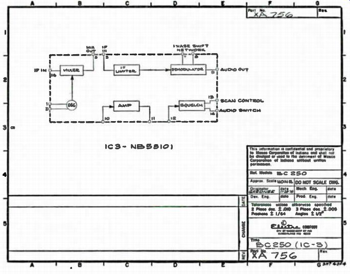
Fig. 8-3. Block diagram of IC3.
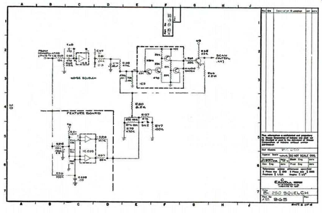
Fig. 8-4. Squelch circuit.
Frequency Detector Squelch
The purpose of this circuit is to keep adjacent channel activity from un-squelching the radio. This would happen in conventional scanner radios in the presence of strong or interfering signals. This circuit will not let the radio un-squelch if the signal is more than 7kHz from received frequency.
The voltage comparator window is set up in IC209 (NB73402 LM358N). The upper voltage limit is on pin 5, the lower voltage limit is on pin 3. These voltages are established by R211, R212, R213, and R214. If a voltage above the upper limit or below the lower limit appears on common pins 3 and 6, the output of pin 1 or 7 will go low. This reduces the voltage at pin 12 of IC3 forcing the receiver to continue scanning. The voltage is within the limits or "within the window"; both outputs will be high. With both outputs high in normal operation, the squelch control R78 is used to set the bias for pin 12 of IC3. If these outputs are high and other squelch conditions acceptable, the radio will be un-squelched.
The discriminator output (IC3 pin 9) develops a DC voltage which is inversely proportional to frequency. The slope of the discriminator is approximately .18 volts/kHz (from the center frequency) and has a DC offset of 2.75v DC. This voltage is filtered by R216 and C209 and serves as the window detector input.
Power Supply
The voltage supply for the Bearcat 250 is developed by the full-wave rectifier circuit of T4, D18, and D19. This develops 16 volts, filtered by C98. The 16 volts is regulated down to 6 volts (A) by R108, R109, and D17 which serves as supply voltage for IC3 and reference for Q21 and Q22 regulator circuits. The 6 volts (A) is applied to the inverting input of each half of IC5 (NB73-401 - MC1458P) so the output of each half will control the base of its associated transistor. The output of each transistor is divided down to 6 volts in the ratio required for +9 volts at the collector of Q22 (always on) and +11 volts at the collector of Q21 (switched). The +9 volts supply from Q22 provides voltage for IC6 and IC8 and is regulated down to +6 by R98 and D16 for voltage reference to IC2 (loop filter) and to maintain power for IC6, 7, and 9.
The unregulated 16 volts is connected to the feature board where it is regulated to +8.4 volts by R220, D210, Q206, and Q204 to supply power to all feature board circuits except IC206 which uses a 6-volt supply derived from +8.4 volts by R219 and D208.
Synthesizer
The Bearcat 250 synthesizer consists of a voltage controlled oscillator (VCO) which is mixed down by 133 MHz (H-U/T) and prescaled before division by a pre-settable counter controlled from memory. The output of this divider is compared to a reference frequency producing an error signal for a loop filter to compensate the VCO voltage to correct the frequency.
Mixer The L or H/U/T VCO signal is coupled through C38 to an emitter - follower stage Q11 which serves as a buffer to drive the low-impedance input at pin 11 of the balanced mixer IC1 (NB85-401, TL442CN). In H or U/T BANDS, the 133MHz oscillator signal from Q13 is coupled through R138 and C42 to the second mixer input at pin 5 of IC1.
The (VCO-133MHz) difference frequency is present at the output pin 3 of I C1 where it is passed through the low-pass filter L19 and amplified by Q23 to drive the prescaler IC6.
On low band, the 133 oscillator does not operate since there is no Q13 base bias from D7 or D8. The second mixer input at pin 5 is also biased up through D6 to permit the mixer to pass the low band VCO frequency. The Low Band VCO frequency is then coupled to Q23 for buffering and amplification to drive IC6.
Prescaler
The input at pin 2 of IC6 (NC57902) is divided by 15 or 16 with the output at pin 11. The division is by 15 when the control input pin 6 is high and by 16 when low.
The prescaler output is connected to pin 7 of IC7 (NB25702) to clock the ÷ N and 12+A counters. Nine memory bits are used for presetting the ÷ N counter and four for the 12 + A counter to provide the proper division at the programmed frequency.
Initially the 12 + A counter output is high and the + N and 12 + A counter is clocked once for each 15 clocks at the prescaler. When 12 + A is reached, the output goes low to allow the prescaler to divide by 16 until the divide by N has reached its full count of 512 = 2 9 ). The ÷ N advances 12 # A times when the prescaler is dividing by 15 and the remainder (512 - M - 12 + A) when the prescaler is dividing by 16.
When the + N has reached full count, it's output goes high to reset itself and the 12 # A counter to start over again. The total division by prescaler and + N is therefore: 15 (12 + A) + 16 [512 - M - (12 + Simplifying, = 8180- 16 M- A
Phase Comparator
The reference frequency for comparison with the +N output is derived from the 10.4MHz oscillator in IC3 controlled by Y2. The 10.4MHz signal is coupled to pin 16 of IC6 where it is divided by 4 for an output of 2.6MHz at pin 11 for an input at pin 5 of IC7. The 2.6MI-Iz signal is then divided by 520 for low or high VHF and by 624 for UHF controlled within IC7 by the U band switch information in memory. This provides a frequency of 5.01cliz on low and high bands and 4.16667kHz (4.16667 x 3 = 12.51khz channel spacing on U/T band) on UHF as a reference for comparing the +N output in the frequency phase comparator.
The phase comparator provides a tri-state output at pin 3 of IC7. This output will go low when the VCO and the +N output is low in frequency.
When the VCO is high in frequency the output will go high. When both are in phase, the phase-comparator has a high impedance output.
Loop Filter
The phase comparator output is filtered and amplified by IC2. R95 and R96 establish a 3-volt bias on pin 5 of IC2 to match the bias on pin 6 provided by R91, 93, and R94. The correction pulses are applied through R89 and R90 and filtered by C85 to the inverting input of IC2.
If the VCO is running too low infrequency, negative correction pulses will go to the inverting input forcing the output DC voltage to go higher.
Meanwhile, C88 in the feedback loop charges to oppose the input change and hold the output at this new level. In the same manner, if the VCO runs too high in frequency, positive correction pulses from the comparator will cause a decrease in the control voltage from IC2 forcing the VCO back down until the +N output is in phase with the reference to stop the correction pulses. When the VCO is on frequency and the comparator output is a high impedance, the charge on C88 will hold the control voltage keeping the VCO at that frequency. Since the width of the correction pulse is dependent on the degree of phase difference, the further the VCO is off frequency, the longer will be the pulse to correct it. D14 and D15 block noise less than 1.4 volts peak to peak coming from the phase comparator when its output is in the high impedance state.
Bandswitching
The bandswitch data from memory is brought out on pins 2 To and 20 (U -') of IC7. When H is low for high band operation, base current for Q15 is supplied through D10 (7.5V Zener) and R51 to turn it on for 11 volts at the collector. Similarly, when U is low, Q14 is turned on through D9 and R49 giving 11 volts at the collector for UHF operation. When IT is HIGH (6 volts) for low band or UHF, D10 does not reach its Zener voltage prohibiting current through it, thereby shutting off Q15. Q14 is shut off in the same manner when U is high for low and high band operation.
The 2.6MHz signal (10.4MHz +4) from IC6 (pin 14) is applied to the input pin 1 of IC9 (NB85-501, CD4520BC). IC9 is a dual binary UP counter with D20 and D21 used to reset the first counter when Q1 (pin 4) and Q2 (pin 5) are high to provide a division by 6. This divide-by-6 output on pin 5 at 433.331d-lz is coupled through R122 to the Control Board as the system clock.
The 433kHz signal at pin 5 is also connected to the input of the second counter at pin 9 of IC9. No reset is used on this section permitting a division by 16 to provide a 27Idiz output at pin 14. The 27kliz output is coupled through R118 and C105 to the input pin 3 of IC8 (NB66801, LM386N) where it is amplified to drive T5. The stepped-up voltage at the secondary of T5 is detected by D22 and D23 to charge C113 to the positive peak voltage to develop a +26 volt source for the tuning voltage amplifier IC2. D24 and D25 detect the T5 secondary to change C114 to the negative peak voltage for a -26 volt supply required for the memory IC202 on the feature board.
Feature Board IC207 (NA65802 - MM57129) and IC208 (NA65801 - MM5782) are a custom programmed microprocessor pair which accepts a decimal keyboard input and converts it to the appropriate binary code for synthesizer control, see Fig. 8-5. These also center the data into memory and multiplex the information for an 11 digit seven segment display.
Keyboard Entry and Display
The decimal keyboard is used to control data inputs Ki, K2, and K3 of the microprocessor which decodes the timing of pulses from the digit scan outputs of IC206. The display data is multiplexed to supply source voltage to each required segment during the sequential strobing of the digit cathodes to display the information. IC208 provides a 4 bit binary code to IC206 (NB86101-DS8968N), a 12 digit decoder/driver which grounds the selected digit cathode. IC205 (NB86201 - DS8654N) is an eight section display driver to supply current for each segment through its associated 100olun resistor in the R221 array.
Hex Latch
Referring to Fig. 8-6, IC201 (NB85801 - MM74C174N) contains 6 D type flip-flops used as latches with a common clock line from F4 of the microprocessor (IC207). Five segment output lines (A, B, C,D, P) from IC208 are also used at F4 clock time to set the latches in the proper state for memory instruction and provide aux. output and mute for squelching the audio during synthesizer data transfer time.
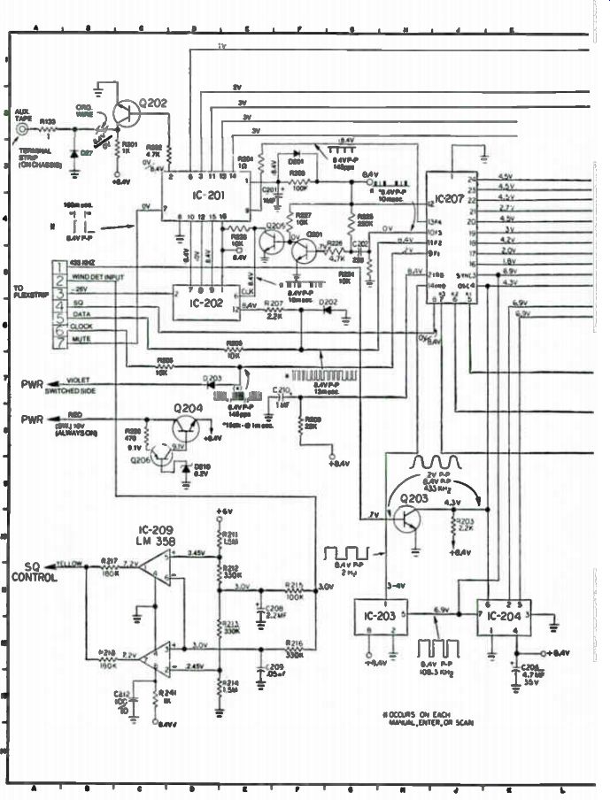
Fig. 8-5. Feature board circuit.
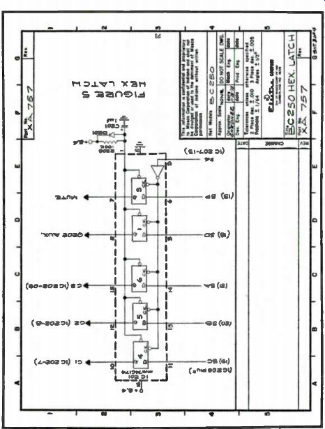
Fig. 8-6. Hex Latch circuit.
Memory
IC202 (NE185901 - ER1400) is a 1400 bit electrically alterable read only memory (EAROM) with a 100 word x 14 BIT organization. Two words (28 bits) are used for each of the 50 channels for frequency, bandswitching delay, lockout, and count information. The device function for each input code from the IC201 latch is shown below.
C1 C2 C3 FUNCTION
0 0 0 Stand By
0 0 1 Not Used
0 1 0 Erase
0 1 1 Accept Address
1 0 0 Read
1 0 1 Shift Data Out
1 1 0 Write
1 1 1 Accept Data
The memory clock is driven from the F3 output of IC207. F2 accepts the serial data from memory and outputs data to the memory and synthesizer (IC7). F 1 provides the clock to transfer data into the synthesizer. When the radio is turned off, Fl is pulled low through D203 to instruct the microprocessor to display time.
Search/Time IC204 (NB86601 - MM57126) is a 1024 bit serial RAM. In the search mode, data is transferred serially into IC204 using 16 bits per search channel. This permits a 64 channel capacity. Data is also transferred serially back into IC208. IC207 contains a sync output for IC208 and IC204 which is the system clock (433kHz) divided by 4 (108.33kHz). The 108kHz SYNC from IC207 is also sent to the clock input of IC203 (N1386001 - MM5369) which is a custom programmed divider. IC203 divides by 54,167 to provide a 2Hz output fed back to IC207. This signal is used by the microprocessor as reference for the real-time clock and the priority sample time.
The complete schematic for the BEARCAT model BC 250 is shown in Fig. 8-7. Also, see Table 8-1. A crystal channel BEARCAT model III is shown in Fig. 8-8.
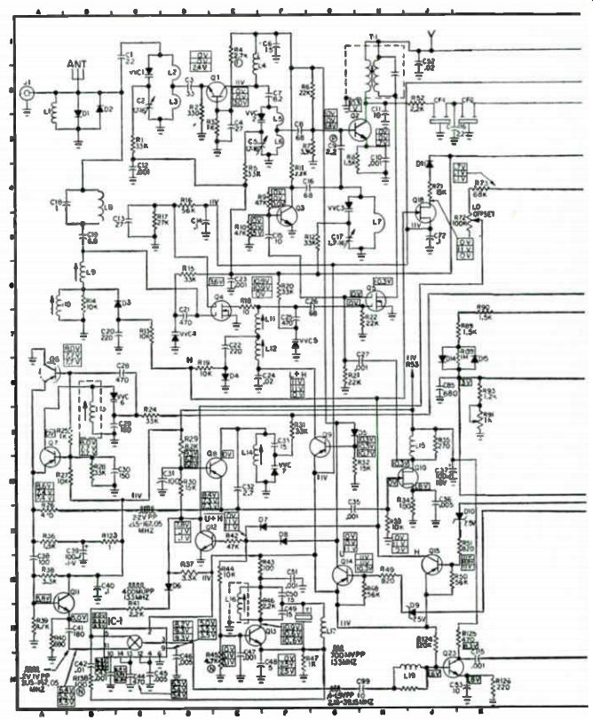
Fig. 8-7. Complete schematic for BEARCAT model BC250.
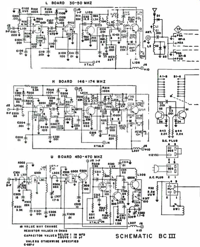
Fig. 8-8. Complete schematic for BEAR CAT III crystal scanner.
----------------- Table 8-1. 8C-250 Symptom & Cure Aids.
Symptom Component
1) No or weak rec. on L band
2) No or weak rec. on H band
3) No or weak rec. on U/T band
4) No or weak I.F.
5) No frequency L band
6) No frequency H & U
7) No squelch or won't un-squelch
8) No audio
9) Power supply
10) Won't program 11) Won't hold program 12) Missing Segments 13) Missing digit 14) No display or dot
No frequencies, 04, 05, band switching No frequencies, Q4, Q5, band switching No frequencies, Q1, Q2, Q3, C2, 5, 17 shorted, band switching IC3, CF 1 , CF2, CF3, Ti, T2 IC6, IC7, Q6 & 7, band switching, 011, Q23 IC6, IC7, Q8, band switching, Q13, Q11, Q23,11 IC209, IC3, D13, Q17, R78 IC4, Open J2, No IF., Q20 (Shorted), IC3 T4, IC5, Q21, Q22, D17, 0204, D210, 016, R98 No - 26V, IC202,10207, IC208, Q205, Q201, IC201 Low -26 volts, IC202, Q201, Q205 IC205, R221, IC208, IC207 IC206, IC208, IC207 Y2, Power supply, IC6, IC9, IC207, IC208, IC203, IC204, 0203, IC3, 0208
--------------
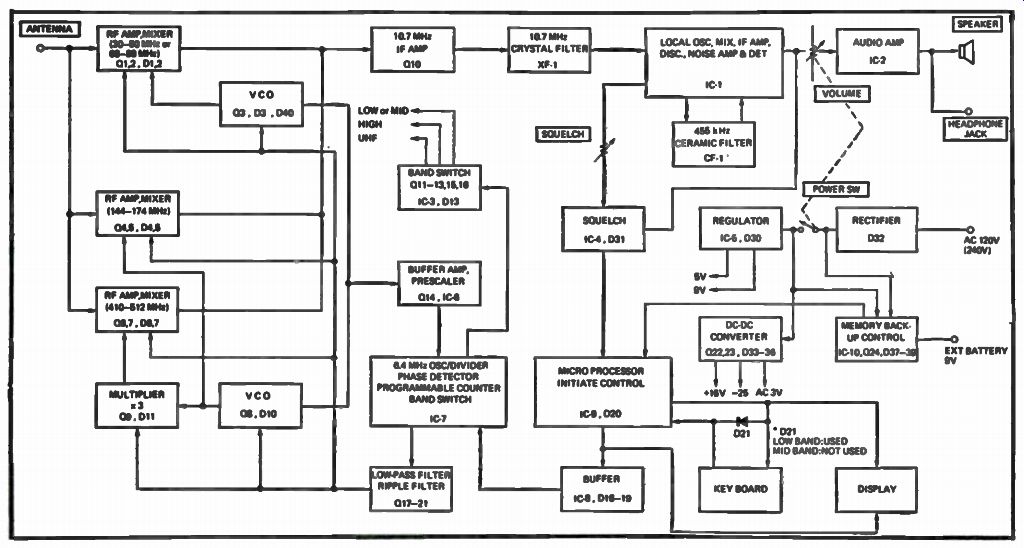
Fig. 8-9. PRO-2008 scanner block diagram.
------------------
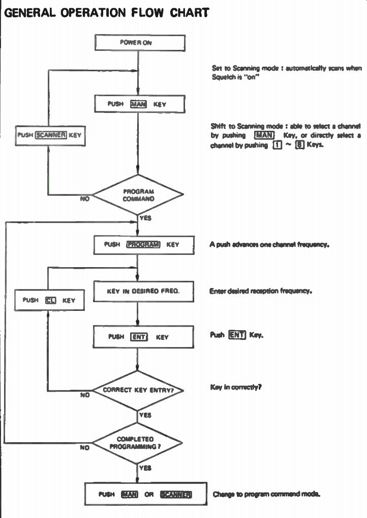
Fig. 8-10. Operational flowchart.
GENERAL OPERATION FLOW CHART POWER ON Set to Scanning 'IN Squelch a On PuSr. reCANNTM KEY PUSH (1 KEY PROGRAM COMMAND YES PUSH [fga:11 KEY PUSH gal KEY
KEY IN DESIRED FREO. PUSH Ecii KEY NO
NO CORRECT KEY ENTRY? VES COMPLETED PROGRAMMING YES PUSH fflla OR EZEMI31
Shift to Scanning ,nods : able to select a cr,n , iel by pushing 'MANI Key. or directly select channel by pushing Ill Keys.
A push admixes one channel heuunx -r.
Enter desired reception frequency.
Key.
Kay in correctly? Change to proem command
-------------------
RADIO SHACK PRO-2008
This scanner is a PLL Synthesized VHF/UHF Receiver, controlled by a Central Processing Unit (CPU). The VHF low band, mid band and high band are received in 5 kHz increments. The UHF band is set up for 12.5 kHz increments. Receiving range, frequency determination, etc., are all functions controlled by the CPU. The CPU is able to do only the assigned functions, and no modification is feasible for this CPU. Circuit Operation Let's now look at the scanner circuit operation in terms of the functional blocks as shown in Fig. 8-9. A general operational flow chart is shown in Fig. 8-10. A variable capacitor diode tuning ("Automatic Tuning System") is used for all bands. Field-Effect transistors (FED are used in the RF/MIX circuits of low, mid and high bands, to achieve optimum mix-modulation and mutual-modulation characteristics. Q10 amplifies 10.7 MHz IF system. A 10.7 MHz monolithic crystal filter is incorporated for better selectivity.
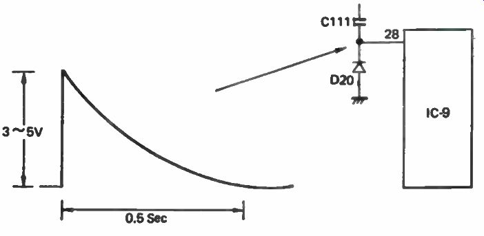
Fig. 8-11. Initializing waveform.
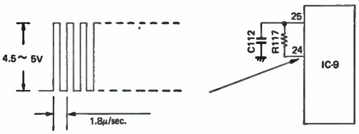
Fig. 8-12. Clock waveform.
IC-1 contains local oscillator, mixer, IF amplifier, discriminator, noise amplifier and detector. The crystal oscillator produces 10.245 MHz, which mixed with 10.7 MHz, results in 455 kHz IF. A 455 kHz ceramic filter is provided to increase selectivity. The 455 kHz IF is amplified in the W Amp stage, and a quadrature FM detector detects it to an audio signal. A portion of the detector output is picked up as a noise product to control the squelch signal level. IC-2 is an audio amplifier.
IC-9 is the central processing unit (CPU). The CPU does data processing, calculation, etc. Unstable supply voltage (VDD) to the CPU can produce CPU malfunction, such as wrong data processing, wrong data transfer, etc. To overcome the malfunctions, D20 and C111 "initialize" the CPU. In case a program backup battery is not connected or is discharged, the CPU may not be initialized by connecting an AC cord to the AC line plug. In such a case, turn the power switch on and push the reset switch on the rear panel to initialize the CPU. Figure 8-11 shows this initializing waveform.
The clock waveform is shown in (Fig. 8-12). The CPU incorporates input terminals, output terminals and HLT terminals. The input and output terminals, along with the keyboard, form a coding network or matrix. The fluorescent display is driven by the 0 and R outputs. The 0 output is connected to the PLL circuit via Q16 through Q19 and IC-8.
IC-7 is a large-scale integration (LSI) IC, which makes up a major part of the PLL circuit. It contains a 6.4 MHz crystal oscillation circuit, a divider to produce 5 kHz/4.166 kHz for the PLL reference frequencies, phase detector, programmable counter, bandswitch, etc. Output from the phase detector controls the voltage controlled oscillator (VCO) circuit, via the low-pass filter Q17 to Q21.
Two VCO circuits for low band and Hi/UHF band are provided. The VCO frequencies are: Low Band or Mid Band = Reception frequency +10.7 MHz.
Hi Band = Reception frequency - 10.7 MHz.
UHF Band = Reception frequency - 10.7 MHz/3.
Thus, VHF and UHF are directly converted to 10.7 MHz, to enable reception with minimum spurious interference. Output from each VCO is injected into each mixer, and a portion of the VCO output is applied to IC-7 (via Buffer Amplifier prescaler) to compose the PLL circuitry.
DC to DC converter consisting of Q22, Q23 and diodes D33 through D36, generates + DC 16 volts, -25 volts, and AC 3 volts and supplies the low-pass filter and display with the respective voltages.