How do field-effect transistors (FET's) work? How do you test one? How can you tell which lead is which if they aren't marked? How are they used in circuits? These and other questions we hope to answer in this two-part series on the field effect transistor.
Conventional transistors (NPN and PNP) are called bipolar transistors because their operation depends on the reciprocal action of two charge carriers (electrons and holes). The FET is called a unipolar device because it uses essentially only one charge carrier (although that carrier may be either a positive or a negative charge, as we will see). Because it is a unipolar device, the basic FET has no sense of direction between its main current terminals, source and drain; that is, the source and drain terminals may be interchanged. Only the gate, which in many respects corresponds to a grid in a vacuum tube, must have a specific polarity of voltage with respect to the source terminal.
How FET's Work
The best way to understand FET operation, I think, is to think of an FET as a "sheet-beam" vacuum tube. That is, the controlling force is a charge that pushes (or some times pulls) the main current carriers out of (or into) a channel. Fig. 1 shows the action of a sheet-beam tube with an internal deflector plate.
Fig. 2 is a circuit diagram of an FET. This is an N-channel FET, which means that the active element has an abundance of negative current carriers (electrons). (Remember that semi-conductor material by nature has a limited number of charge carriers, unlike a piece of wire, for example, which has an almost in finite number of charge carriers.) Let's first consider Fig. 2A. At each end of the N-channel material is a connection to the semiconductor. One of these connections is called the source and the other the drain. Because of the current carriers in the "N" material, current can flow through it in either direction, depending on which way the battery is connected. Because of the limited number of current carriers in the channel, the channel looks not like a piece of wire but more like a 1000-ohm resistor.
Next, consider Fig. 2B. Here a new element is positioned between the source and drain. This element is called a gate. Like any gate, it can be completely open or shut or one quarter open, half-way open, etc.
In an FET, ideally, there is a high resistance between the gate and the channel. The gate may be a piece of P-type material with a reverse bias, or there actually may be a very thin slice of insulation between the gate and the channel.
With the gate tied to the source, as in Fig. 2B, current continues to flow just as if the gate were not present.
Next, let's consider Fig. 2C. When a negative bias voltage is connected between the gate and source, the current between the source and drain of the FET de creases. What has happened? The negative voltage on the gate repels the electrons (negative charge) in the channel and forces them toward the substrate. This leaves fewer current carriers available in the channel, and less current flows. In other words, the original "1000-ohm resistor" now looks like a 5000-ohm resistor. Applying a negative charge to the gate of the FET has caused the resistance of the channel to increase. Fig. 2D shows what hap pens if the negative voltage on the gate is increased enough. The current flow is completely "pinched off" between the source and drain.
This is because all of the electrons have been forced out of the con ducting channel.
No mention has been made of gate current flow. The reason? There is none! The flow of current between the source and drain is con trolled by a voltage charge. This is why the FET, like the vacuum tube, has a high impedance . . . it requires no power in the input to control power in the output. The similarity that exists between vacuum tubes and FET's is reflected in the circuitry used with FET's, as you will see in next month's article.
Types of FET's
As mentioned previously in this article, there are two general types of gate structures. First, there is the junction FET (j-FET) which has the gate "junctioned" into the channel in much the same manner as a PN junction of a diode or bipolar transistor. This type of FET has the advantages of simplicity, ease of testing with an ohmmeter, and little likelihood of static-charge damage (to avoid such damage, the leads of some FET's must be kept shorted together until the FET is installed in the circuit). In the j-FET, the gate is reverse-biased by the circuit so that only a very small amount of current flows between the gate and channel.
The other general type of gate structure is itself divided into two distinct types: The MOS (metal-oxide semiconductor) and the IG (insulated gate), often referred to as MOSFET's and IGFET's. In these, the gate is actually insulated from the channel by an extremely thin layer of oxide. This insulation prevents current flow to the gate, whether it is positive or negative with respect to the source terminal.
The input resistance of the MOS FET's and IGFETs can be in the hundreds of megohms.
Since the insulating coating between gate and channel is so thin, there is a danger of "static puncture" of the coating. Enough static charge can build up on an open gate lead to pierce the coating and make a high-resistance connection between gate and channel. (When this happens, the transistor often can still be used as a junction transistor by applying a reverse bias to the gate.) Other Types and Classifications In addition to the j-FET's, MOS FET's and IGFET's, any of these various types may use either an N or a P-channel. Basically there is no difference in the channel type, except that the gate bias is opposite for the two.
So far we have talked only of depletion FET's, in which a bias on the gate causes the current to be depleted or decreased. Insulated-gate transistors may also have an enhancement mode, in which the current is increased by a charge on the gate; in other words, more current carriers are pushed or pulled into the channel by the gate voltage rather than pushed out as in the depletion mode.
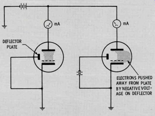
Fig. 1 Simplified action of a sheet-beam vacuum tube. The "gating" action
of field-effect transistors is similar to that shown here.
How FET's are Used JFET
The junction field-effect transistor (JFET) operates with a high impedance input only as long as the gate-to-channel diode is reverse biased. Circuits using JFET's use either fixed- or self-bias (Fig. 3) to make sure the signal input does not forward bias the gate. For an N channel JFET, the bias from gate to source is negative, and on a P-channel JFET it needs to be positive, as shown in Figs. 3 and 4.
MOSFET
Metal-oxide semiconductor field effect transistors (MOSFET's), which are sometimes called insulated-gate field-effect transistors (IGFET), can operate with both re verse and forward bias voltages applied between gate and source. For example, no bias is used in the circuit in Fig. 4. The input signal can go both positive and negative with out causing distortion in the output.
This is because no gate current can flow; when the gate goes positive, the source-to-drain current simply is increased above the zero bias value. When the gate signal goes negative, the source-to-drain current is reduced much like it would be in a JFET circuit.
This JFET type of operation, in which the bias is sufficient to pre vent the input signal from producing forward bias, is called type A operation. MOSFET's can be, and often are, operated in this mode, even though it is not necessary.
The circuit operation that permits both a positive and negative excursion of the signal voltage on the gate of the MOSFET is called type B. (Because JFET's would draw gate current if forward biased, they normally do not operate in the type B mode.)
-----------------
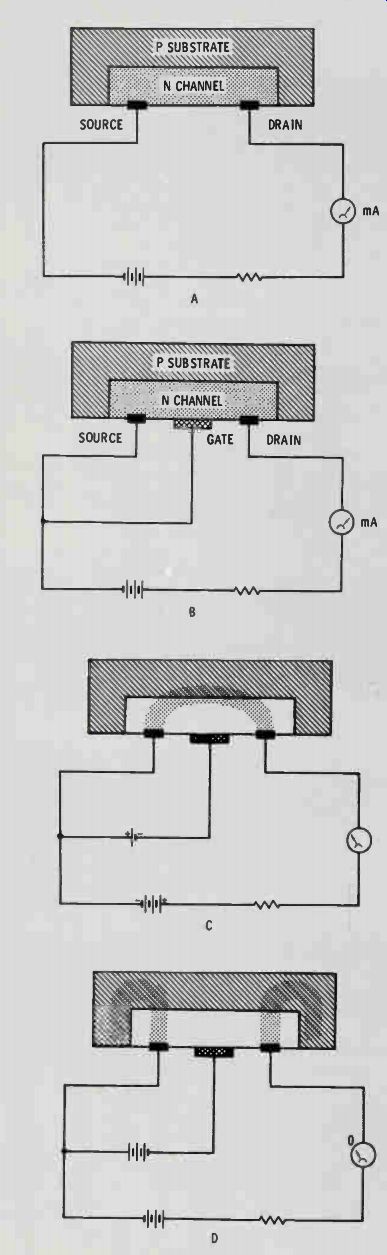
Fig. 2 Circuit dia grams showing construction and operation of N-channel FET.
A) Current can flow in either direction in region between source (cathode) and drain (plate). Limited number of current carriers made this region appear as a 1000-ohm resistor.
B) Variable control element called a "gate" is positioned between source and drain.
C) Current flow between source and drain is reduced when a negative bias voltage is applied between gate and source elements.
D) Complete “pinch off" of source-to drain current is accomplished by gate when gate bias is high enough to force all electrons out of conducting channel.
------------------
Certain kinds of MOSFET's are called depletion types (all JFET's are depletion types) because they produce current flow with zero bias, and additional gate bias will reduce this source-to-drain current.
Other MOSFET's are known as enhancement types, which have virtually zero source-to-drain current until they are biased on. For example, the source-to-drain current might be no more than a micro ampere at zero bias, but when a +1 volt is applied to the gate, the source-to-drain current will increase to about 1 milliampere. This action is comparable to that of the familiar bipolar conventional transistor, which must be forward biased be fore current flows between emitter and collector. The difference is that the MOSFET, because of the insulated gate, has a very high input impedance (up to 100 megohms or more).
Operation in the enhancement mode is called type C. (See Fig. 5.)
The insulated gate of the MOSFET gives it exceptional isolation between the input and output circuit (even considerably better than a tube). MOSFET's used as radio-frequency amplifiers in radios are less susceptible to cross-modulation interference; that is, they can operate among several strong local stations with less chance of beats, whistles, or stations coming in at more than one place on the radio dial.
The dual gate FET (see symbols in Fig. 10) can be used as a mixer, and has better isolation than a twin- grid tube.
Fig. 5 is an example of a circuit that is difficult to design using al tube, almost impossible with a bi polar transistor, but which is easily adaptable to the FET. This is a remote volume-control circuit that uses pure DC voltage to control amplifier volume from almost any distance. The signal input is fed to the drain terminal of the control FET through a 1-megohm resistor. The source terminal is tied to ground. By applying more or less negative voltage to the gate, the FET changes from high to low resistance. The equivalent circuit in Fig. 6B shows how this shunt circuit works. Increasing the negative voltage to the gate increases the source-to-drain resistance, less signal is bypassed to ground, and the volume increases. Note that there is no need of any DC voltage between the source and drain.
Fig. 3 JFET's are depletion-type FET's; that is, source-to-drain current can
flow with no bias applied to the gate. Control of the source-to-drain current
is accomplished by reverse biasing the gate, which reduces or completely cuts
off source-to-drain current, depending on the amount of reverse bias applied.
Either fixed- or self-bias is employed to assure that the input signal does
not forward bias the gate and cause it to draw current. A) N-channel JFET with
fixed bias applied to gate. B) P-channel JFET with fixed bias. C) N-channel
JFET circuit employing self-biasing, which, in this case, is the voltage developed
across resistor RS. The bypass capacitor, CS, may or may not be used, depending
on how degeneration affects the function of the circuit. D) Self-biased P-channel
JFET.
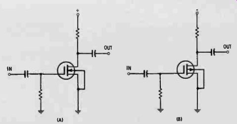
Fig. 4 Metal-oxide semiconductor field-effect transistors (MOSFET's) can operate
satisfactorily with both reverse and forward bias voltages from gate to source
because the insulated gate prevents the flow of gate current when the voltage
on the gate swings positive. A and B show depletion MOSFET's connected for
type B mode of operation (gate voltage can swing both positive and negative).
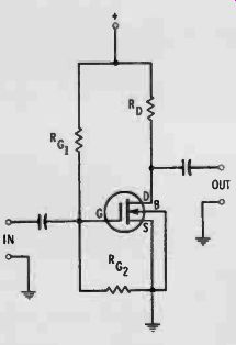
Fig. 5 Circuit employing enhancement MOSFET biased to operate in the type
C mode (little source-to drain current until gate potential is increased in
positive direction). RG1 and RG2 form a bleeder circuit to supply turn-on bias
to the gate. If you zero-bias the gate by connecting a jumper from gate to
source, the source-to-drain current will be reduced to near zero, or about
1 microampere.
Comparison of Circuits
Fig. 7 shows three comparable circuits using a FET (A), a bipolar transistor (B) and a tube (C) in a simple RC audio amplifier circuit. Note that the FET and tube circuits are almost identical except for the size of the supply voltage. The bipolar transistor differs from the other two, both in method of biasing and in the amount of in- put impedance. The lower input and output impedances of the bipolar NPN transistor mean that resistors used in the circuit are smaller in value, and capacitors are much larger than those used in either the FET or tube circuits.
For example, in the FET and tube circuits shown in Fig 8, CC, and CC2 could well be around .005 to .01 mfd, while in the bipolar transistor circuit the capacitors likely would be 2 mfd or more. The load resistor of the bipolar transistor likely would be no more than 10K, and probably less, while the load for the FET and tube would be 15K to perhaps 470K or more.
The input impedance of the FET and tube will be as high as the input resistor; the input of the bi polar transistor probably will be no more than about 1000 ohms.
Both the FET and the bipolar, in most cases, will operate satisfactorily on lower supply voltages than those needed by the tube. The power output of the amplifier using a bipolar will be higher than either the FET or tube because it will draw more current, but the FET or tube are better voltage amplifiers.
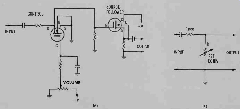
Fig. 6 A MOSFET circuit for remotely controlling volume. A) Actual circuitry.
B) Equivalent circuit.
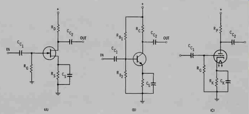
Fig. 7 Comparison of FET, bipolar transistor and tube circuits. Tube and FET
circuits are similar except fcr values of sup ply voltage. Bipolar transistor
requires lower supply voltage, smaller values of resistance and larger values
of capacitance than other types of circuits shown here. A) FET, B) bipolar
transistor and C) tube circuits.
Testing FET's
If you service, or expect to ser vice, a number of FET circuits, you should treat yourself to a FET tester. Most new bipolar transistor testers also make FET tests. You can, though, make a fairly valid test of any JFET using just your ohmmeter.
Comparison of Circuits
Fig. 7 shows three comparable circuits using a FET (A), a bipolar transistor (B) and a tube (C) in a simple RC audio amplifier circuit.
Note that the FET and tube circuits are almost identical except for the size of the supply voltage.
The bipolar transistor differs from the other two, both in method of biasing and in the amount of in put impedance. The lower input and output impedances of the bipolar NPN transistor mean that resistors used in the circuit are smaller in value, and capacitors are much
Although not all JFET's are sym metrical (drain and source terminals interchangeable), most are. If you encounter an unmarked FET, or if you're not sure whether it is a FET or a bipolar (since they use the same kinds of metal and plastic cases), you can use an ohmmeter to find out if it is really a FET, and which lead is which. To do so, measure with an ohmmeter (the R X 10 range is a good one) between any two leads. Note the reading, and then reverse the test leads and connect them to the same FET leads as before. If the two readings are the same (maybe around 1000 ohms), the two leads are the drain and source terminals of the FET., The other lead will be the gate. The' gate of the JFET will have diode action to either the source or drain terminal (high and low resistance readings when you reverse the ohm meter leads while measuring between the gate and the drain or source). Is it an N channel or P channel? That's easy, too, if you know your ohmmeter. An N channel will produce a high resistance if you place a negative voltage between the gate and the source or drain. A low resistance will be indicated if you place a positive voltage between the gate and the source or drain of the N channel.
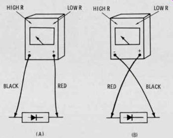
Fig. 8 Method for deter mining whether "+" lead for voltage function
of VOM also is "+" lead for resistance function.
A) If ohmmeter indicates highest resistance with leads connected as shown, red lead of VOM also is "+" lead for ohmmeter function. B) If ohmmeter indicates highest resistance when connected in this manner, red lead of VOM is negative lead for ohmmeter function.
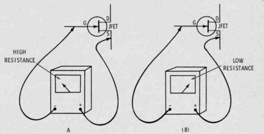
Fig. 9 Readings obtained using American and Japanese type VOM's to deter mine
type of channel of FET (N in this case). A) American VOM. B) Japanese VOM.
The ohmmeter supplies this positive or negative voltage, but herein lies a pitfall: On most American made ohmmeters, the "+" lead for measuring voltage will also be the "+" lead for testing ohms.
However, on most Japanese-made meters, the "+" red lead for the voltmeter is tied to the negative side of the ohmmeter battery when measuring ohms.
Fig. 8 shows how you can determine which of the preceding ways your meter is connected on the ohms function. Once you find out, all you have to do is remember which ohm meter lead is positive. Fig. 9 shows how an American type and a Japanese type VOM will check the same N-channel JFET. MOSFETS are not easy to check with an ohmmeter, though you can determine which is the drain, source and gate terminal. The gate terminal is a complete open circuit to either of the other two leads.
CAUTION: The oxide insulation in a MOSFET is very thin and delicate. The gate lead should always be returned through a resistance to the source terminal; otherwise it can pick up enough static electricity to puncture the insulation. MOSFET's should be stored with the leads taped or twisted together, and should be kept this way until after being installed in the circuit.
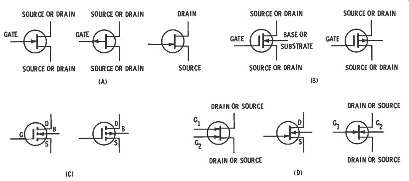
Fig. 10 There is never complete standardization of symbols for electronic
devices, and certainly not while the device is relatively young. But in general,
the symbols for FET's are similar enough so that they can be recognized. A)
The JFET symbols are relatively well standardized. As in all transistors, the
arrow points to "N" material. The N-channel FET is on the left and
a P channel FET on the right. The arrow is on the gate terminal. The N-channel
JFET is normally biased negative from gate to channel; the P-channel type is
normally biased positive. B) Symbols for the depletion-type MOSFET's or IGFET's.
These FET's have a very thin oxide coating between the gate and the channel.
The oxide acts as an insulator, and no current can flow between the gate and
channel, regardless of the direction of the bias voltage. The arrow of the
symbol shown is not on the gate terminal but on the substrate or base (not
to be confused with the base terminal on a bipolar transistor). Again, the
arrow indicates whether the transistor is an N- or P-channel type. C) Symbols
used for enhancement type MOSFET's. As explained in December, the enhancement
type requires bias voltage on the gate to start current flow between the source
and drain terminals, while the depletion type requires bias voltage to reduce
or pinch off the current flow between source and drain. D) Symbols for dual-gate
FET's. On the left is an N-channel symmetrical type (drain and source are interchangeable).
In the center is an other symbol for the N-channel non-symmetrical type (drain
and source are not interchangeable).