The design of tube voltage amplifier stages is essentially a simple task by comparison with much solid state linear circuit design, if only because there are not many circuit options open to the designer of tube circuits. Tubes are also relatively linear in their input/output transfer characteristics, and therefore require less in the way of circuit design elaboration to improve the circuit performance and reduce any residual waveform distortion.
Circuit Configurations
For tube operated low frequency amplifier stages the only real choice is between triodes and pentodes. Both of these tube types can be employed in one or other of the five circuit arrangements shown in simplified form in FIG. 1 -- grounded cathode, grounded grid, cascode, long-tailed pair and cathode follower, sometimes called grounded anode. For simplicity, I have shown at this stage only the triode tube versions of these circuits.
In the case of a normal (grounded cathode) triode voltage amplifier stage, of the kind shown in FIG. 1a, the major choices to be made are between the type of grid bias system which is used and the type of anode load which is employed to convert the changes in anode current, brought about by changes in the control grid voltage, into a signal voltage output.
Grid Bias Systems
A graph showing the relationship between the anode current and the grid voltage
in a typical small-power triode amplifier tube (one half of an ECC83 double
triode) is shown in FIG. 2. It is required, for the lowest possible amplitude
distortion in the output signal waveform, that the tube should be operated
on the most linear part of its Ia/Vg characteristic curve. This implies that
the grid voltage will not be driven so far negative, during the input voltage
swing, that it runs into the curved region of this characteristic, near I a
cut-off, nor will it be allowed to become positive in relation to the cathode
voltage, when grid current would flow, and the grid would cease to offer a
high input impedance. An additional consideration is that the actual anode
current should be chosen- if there is, within the desired distortion criteria,
a range of current levels at which the tube could be operated equally well
- to be the lowest current level within this range. This should be done to
minimize the waste of energy in excessive anode dissipation, and to avoid any
needless reduction of cathode life, a thing which has an inverse relationship
with anode current.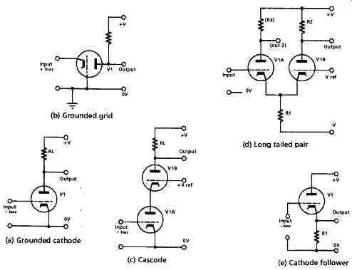
FIG. 1 Tube gain stages (b) Grounded grid (a) Grounded cathode (c) Cascode
(d) Long tailed pair (e) Cathode follower
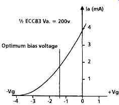
FIG. 2 Anode current vs. grid voltage -- Optimum bias voltage
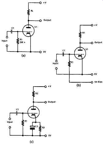
FIG. 3 Tube biasing systems
The static working voltage applied to the grid will normally be provided in one of three ways, as shown in FIG. 3. The simplest of these, illustrated in FIG. 3a, takes advantage of the fact that there will be random collisions between the electrons in the 'space charge' surrounding the cathode and the control grid wires, even if the control grid is slightly negative in respect to the cathode. If a grid resistor (R1) of 2 megohms or greater is used, the grid current (perhaps 250pA) flowing through this will cause the grid to acquire a small negative voltage (perhaps 0.5V) in respect to the cathode, which will probably be adequate for a small-signal input stage. This arrangement has a number of advantages in small-signal circuitry, in addition to its simplicity, of which the major one is that it provides the highest gain figure for a given anode load impedance. The low cathode circuit impedance of this layout also assists in keeping 'hum' and noise to a low level.
This advantage is shared by the fixed bias arrangement shown in FIG. 3b, in which any convenient value of input resistor (R1) can be used, provided that it is not so high that grid-current biasing also occurs. This layout is invariably used in directly heated (battery operated) tube circuitry, where all the cathodes (which will be directly heated filaments) will be operated from a common supply, and is occasionally used in power output stages because it will allow a slightly greater output power to be obtained for the same distortion level than would be given by a similar output stage using cathode bias. For example, Mullard quote an output from a push-pull pair of EL91 output pentodes of 4 watts, at 3.3% THD, whereas 4.8 watts could be obtained, at the same distortion figure, if fixed bias were used. A similar relationship in respect of the maximum output power levels for fixed and cathode bias arrangements exists with the KT66 and 6L6 output beam-tetrodes.
In practice, the circuit layout shown in FIG. 3c is by far the most widely used method of generating the required level of grid bias for an indirectly heated tube. In this arrangement, a resistor (R3) is included in the cathode circuit so that the cathode current will cause the cathode voltage to rise so that it is positive to the control grid- which will be the same, in effect, as the grid being negative with reference to the cathode.
If there is no bypass capacitor across R3 the presence of the cathode circuit resistor will somewhat reduce the gain of the stage. This is due to the local negative feedback caused by the appearance at the cathode of a small AF signal, which acts to reduce the effective input signal voltage. Since the cathode resistor R3 is effectively in series with the anode circuit resistance (R2 in parallel with Ra) the feedback factor (Beta) will be:
β = R3/(R2//Ra)
(in this I have used the symbol//to mean in parallel with). If we take the case of the ECC83 triode referred to previously, at Va = 150V, then Ra = 47,000-ohm and the amplification factor (u) will be 100. If we make R2 the same value as Ra, then the stage gain, without any cathode circuit feedback, called Ao will be given by the relationship:
Gain = μR2/(R2 + Ra) = 100
47k/94k = Ao = 50
However, if we make R3 a 1k-ohm resistor, then Beta (β) will be:
R3/23.5k = 0.042
The expression for gain with feedback (A') is
A’= Ao/(1 + β Ao) = 23.8
which shows that the presence of an unbypassed cathode resistor will reduce the stage gain to a significant extent. The normal technique employed to lessen this drawback is to connect a capacitor (C2) in parallel with R3. At AC, the impedance of the capacitor will be:
Zc = 1/(2 pi fC)
...where f is the operating frequency. For example, a capacitor of 220uF will have an impedance of 36ohm at 20Hz, and the effect of this in parallel with the 1k-ohm cathode circuit resistor will be to increase the stage gain to 46.5. This will still cause a small reduction in the LF response, and, if this is important, a larger value could be chosen for C2. At high audio frequencies the impedance of the bypass capacitor will be so low that the effect of the cathode circuit components can be neglected.
A further disadvantage in the use of cathode bias arrangements in comparison with fixed bias systems (where the cathode is tied to the 0V rail) is that the voltage developed in the cathode circuit is effectively subtracted from the anode supply voltage, and will reduce the possible undistorted anode voltage swing. This is a factor which should be considered in tube amplifier output stage design.
Cathode Bias Resistor Calculations
If the chosen amplifying device is one half of a ECC83 double triode, the required value of cathode bias resistor can be determined approximately by calculating the value of anode load resistor across which the voltage drop will place the quiescent anode voltage at about half the +V supply line potential. However, in order to determine this one must first choose a level of anode current which will place the operating point for the tube somewhere about the middle of the straight portion of the Ia/Vg relationship shown by the manufacturers (2mA at-1.4V). If the +ve supply voltage is 300V, and the anode load resistor is 75k-Ohm, the quiescent anode voltage will be 150V, at this value of anode current. A cathode bias resistor of 700-ohm would then be required to provide the required-1.4V cathode bias. Unfortunately, the characteristic Ia/Vg curve shown for the tube is that for a +200V anode voltage rather than a + 150V one, as presumed in our calculations, and this lower anode voltage will reduce the anode current flow, which will, in turn, require a slightly lower value of both cathode bias and cathode bias resistor- say 620 ohm rather than 700 ohm. However, the tube manufacturers will often quote a recommended value for the cathode bias resistor for a given anode load resistor and supply voltage.
Anode Load Systems
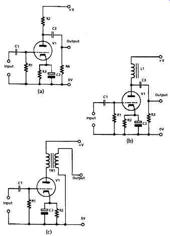
Although the resistor/capacitor circuit shown in FIG. 4a is by far the most commonly used inter-stage coupling layout, in that it allows a wide gain bandwidth and straightforward phase/frequency relationships, the circuit stage gain is still further reduced in comparison with the simple model of FIG. 3c because, assuming that the impedance of C3 is small enough to be neglected, the anode load resistance seen by V1 is that of R a in parallel with both R2 and R4. It is also evident that there will be a voltage drop across R2, which will reduce the anode current for a given level of grid bias, the amplification factor (u) and the mutual conductance (gm) of the tube, since all of these parameters are anode voltage dependent.
The use of an LF choke, L1, as the anode circuit load, as shown in FIG. 4b, offers an increase in stage gain in comparison with the simple resistor coupled arrangement because the DC winding resistance of the choke and the voltage drop across it will probably be low enough to be neglected. Also, if the anode current of V 1 is modulated so that it swings both below and above its quiescent level, the output voltage, as seen at the anode of V 1, will swing both above and below the level of the +V rail, and, for this reason, can probably give an output voltage swing rather more than double that of the circuit layout shown in FIG. 4a.
The major disadvantages of the choke/capacitor inter-stage coupling system are that the phase/frequency characteristics of the choke impedance are very complex- due to the characteristics of the core material, the leakage inductance of the windings, which will either be in the form of segments or layers, and the inter-winding capacitances - and these effects will impair both the distortion characteristics and the flatness of the frequency response of the stage. This will limit the extent to which it is possible to use overall negative feedback to improve the performance of a complete amplifier.
The use of an inter-stage transformer coupling, as shown in FIG. 4c, suffers from all the snags of choke/capacitor coupling, but will allow an even greater increase in both stage gain and possible output voltage swing in comparison with FIG. 4a.
This made it a very popular arrangement in the early years of electronic audio amplifier designs in which it was sought to keep the number of tubes used to as few as practicable. Transformer designs of that period offered voltage step-up ratios from 1:2 to 1:7 (in general, the lower step-up ratios offered better audio performance) and this could give, for example, a two tube amplifier design enough gain to drive a loudspeaker from a piezo-electric gramophone pick-up input. A particular advantage of an inter-stage coupling transformer was that, if the secondary winding was center- tapped, the input stage could be made to drive a push-pull pair of output tubes, which offered much greater output stage efficiency and output power. This topic is examined at greater detail in the section dealing with phase splitter arrangements.
Grounded Grid Stages
This type of circuit layout, shown in FIG. 1 b, mainly found use as an RF amplifier - in which it was effective up to very high frequencies - because the earthed control grid would act as an electrostatic screen between the output and the input circuits, which would avoid the problems due to unwanted signal feedback through the inter-electrode capacitances.
The advantages of this type of stage are that its input/output transfer characteristics are very linear when used with an input current source, or any other high impedance signal source, and that, as already noted, there is almost complete isolation between the input and output circuits. The main problem is that the input impedance (Rin) as seen at the cathode, is very low--approximately 1/gm, for an impedance in k-ohm if the gm is measured in mA/V. This could be as low as 200 ohm for a tube with a mutual conductance (gm) of 5mA/V. A further problem is that any current leakage between the heater and cathode circuits will inject hum and noise into the input signal path.
Tubes such as the E88CC were made especially to avoid this problem in grounded grid and cascode layouts.
Since the anode (Ia) and cathode (Ik) currents will be substantially identical, the output voltage (Vout) will be:
V out = IaR1 = IkR1 If the input impedance (1/gm) is low enough in comparison with the source resistance (Rs) that it can be neglected, then the stage gain will be:
Vout/ Vin IaR1/IkRs= R1/Rs
In other words, the grounded grid stage will only provide more than unity gain if the source impedance is less than the load impedance. The anode impedance (Ra) of the grounded grid stage is very high, approximately uRin.
The Cascode Circuit
This circuit arrangement, shown in FIG. 1c, has all of the advantages, such as linearity and input/output circuit isolation, which are associated with the grounded grid layout, but with the added benefit that the input impedance is very similar to that of the conventional grounded cathode layout of FIG. 1 a. A small disadvantage of the cascode layout is that an additional voltage supply to V1B (shown in the diagram as +V ref) is needed, and since this must allow V1A enough anode voltage (say 60V) to operate satisfactorily (the Va of V1A will be typically Vref +1.5V) the supply voltage available to V1B will be reduced by this amount, with a consequent reduction in the possible output voltage swing in comparison with the layout of FIG. 1a.
As is the case with the grounded grid amplifier, the anode resistance (Ra) of V1B is very high because its anode current must be the same as its cathode current, and this is simply the anode current of VIA, which will be largely unaffected by the anode voltage of V1B. Because of the passive operation of V1 B, the characteristics of the cascode stage are determined by the operation of VIA, and that component of non- linear distortion in a tube amplifier which is due to the effect of variations in anode voltage on the anode current is very much reduced because the anode voltage of V1A is clamped to a fixed level by the cathode follower action of V1B.
As with the grounded grid layout, a tube type designed for cascode applications should be employed, where possible, in this application to minimize the intrusions of 'hum' and noise from the heater supply line into the cathode circuit of V1B. With modem technology, it would be easy to reduce the extent of this problem by operating the heater circuit of V1B from a stabilized DC supply line.
The Long-tailed Pair
The circuit layout shown in FIG. 1d should perhaps be called a cathode coupled amplifier, but the term long-tailed pair is so widely used that other descriptions seem pedantic. As in the cascode layout, the amplifying tube operates as a grounded grid stage, with its grid, in this case, being held at a fixed voltage by a low impedance DC source (which could be the 0V rail if the tail resistor is taken to some suitable negative supply line), and with the signal input being injected into its cathode circuit.
A practical disadvantage of this circuit is that the stage gain of this arrangement is approximately half that of the simple grounded cathode layout of FIG. 1a. This comes about because both V1A and V 1B act as cathode followers in relation to the tail resistor R1. While V1A seeks to transfer the input signal present at its grid to its cathode rail, V1B seeks to hold this cathode rail voltage at a fixed and constant voltage.
If both triodes are identical in their characteristics the result of these opposing endeavors will be to produce a signal voltage change at their cathodes which is half that of the input signal amplitude, at V1A grid.
A useful feature of this circuit arrangement is that, if the cathode tail resistor is sufficiently high, and if both anode circuits have identical load resistors (for simplicity, in FIG. 1d, I have only shown one (R2) in V1a's anode circuit) the signal voltages developed at the two anodes will be very nearly equal in amplitude but in phase opposition. This allows such a stage to be used as a phase splitter preceding a push-pull output stage- this offers a great improvement in performance in this function in comparison with an inter-stage coupling transformer with a center-tapped secondary winding. It also allows the input to be directly connected to the grid of V1A, since the reference voltage at the grid of V1B can be adjusted to give the correct balance between the two tubes.
The Cathode Follower
This circuit layout is shown in FIG. 1e, and normally gives a low impedance output at a voltage gain which is slightly less than unity. The actual output voltage can be calculated by treating the circuit as a simple amplifier with a gain Ao and 100% negative feedback (i.e. Beta = 1). In this mode, using half of an ECC83 double triode, the gain with feedback (A') will be:
…and the output impedance will be approximately 1/g_m ~= 600ohm.
An input DC bias voltage will normally be chosen so that an appropriate level of cathode current will flow and will maintain the DC operating point of the tube at a suitable position on its Ia/Vg curve. The main use of the cathode follower is to transform an input signal at a high impedance into a virtually identical signal at a low impedance, without the need for an iron cored transformer, which would introduce unwanted distortion and phase/frequency errors.
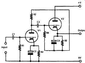
Fig. 5 The u follower
The μ (mu) Follower
This circuit, shown in FIG. 5, has been recently reintroduced as a way of getting an increased stage gain from an amplifying tube (V1) by using a cathode follower (V2) as an active anode load. The cathode follower circuit gives a low output impedance, and as an active load it effectively increases the stage gain of V 1. The snag is, as with all output load increasing systems, that the inter-electrode and other stray capacitances associated with the grid and cathode circuit of V2 will then have an increasingly important effect on the gain of the system, which will decrease as the signal frequency is increased. Also, an upper limit to the available gain is imposed by the shunting effect of the anode current impedance (Ra) of V1. A small-signal pentode, which will have a higher value of R a than a triode, would be better as the input tube, V1.
Tetrodes, Beam-tetrodes and Pentodes
In the early days of tube radio receivers it was found that the triode tube was unsatisfactory as an amplifier at high frequencies because the unavoidable internal anode/grid capacitance of the tube would cause RF instability, particularly with inductive input and output circuitry.
An engineering solution to this problem was found in the introduction of a fine mesh grid, interposed between the control grid (G1) and the anode, connected to a low impedance voltage source, and held at a positive potential with respect to the cathode.
This would act as an electrostatic screen between the anode and cathode and virtually eliminate the anode/grid capacitance. Since this grid was positively charged it would not significantly affect the cathode current of the tube.
The effect that this had upon the tube characteristics was to reduce the influence of the anode voltage upon the anode current. This caused a great increase both in R a, to perhaps several megohms, and also in the magnification factor (p), which could be as high as 5000, though because this depends so much on other things it is not often quoted by the manufacturers, and seldom used in stage gain calculations, for which the relationship Ao = gmR1 is normally employed rather than Ao = μR1/(R1 + Ra). Although the tetrode, or screened grid tube, provided an effective answer to the problems of instability in RF amplifier stages it was unsatisfactory for use as a small-signal audio amplifier stage, except at low output signal voltage levels, because of the kink in the tetrodes Ia/Va characteristics. This kink occurs for the following reason. In any tube some secondary electrons will be emitted from the surface of the anode when high velocity electrons (from the cathode) impinge on it, especially if its surface has become contaminated with cathode metals. In a triode, this effect is unimportant because there is nowhere that such electrons can go, apart from returning to the anode.
In a screened grid tube, however, these electrons will be attracted to the positively charged screening grid, which will effectively reduce the electron flow to the anode, and this will result in a downward dip in the anode current curve, as shown in FIG. 6.
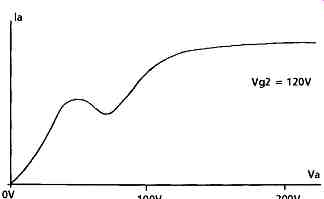
FIG. 6 The 'tetrode kink'
Two solutions were found for this problem, of which the simplest and most widely adopted was the introduction of an open-mesh suppressor grid between the anode and the screening grid (G2). If this grid is connected to a point having a negative potential with respect to the anode - normally the suppressor grid (G3) is connected, either internally or externally, to the cathode - the decelerating potential between this electrode and the anode will cause the secondary electrons to fall back upon the anode, and the kink due to secondary emission from the anode disappears.
The second, more elegant and more expensive, solution to this problem was the so-called kinkless tetrode design, invented by the Marconi-Osram Valve Company. In this arrangement, shown in FIG. 7, a pair of beam-confining plates, connected to the cathode, were interposed between the grids and the anode so that the electrostatic field pattern due to their shape would discourage any electron flow back towards the screening grid (G2). As a further improvement, the two sets of grid wires of the tube (G1 and G2) were aligned so that electrons from the cathode were formed into beams, and those which had passed between the control grid wires would generally fly past the screening grid wires as well, without collision.
The advantage of this structure was that it brought about a reduction in the current flow to G2, by comparison with a pentode structure, and the G2 current is just wasted energy, which contributes nothing to the design except heat. It also offered a lower distortion than an equivalent output pentode, especially when G2 was connected to the anode, to simulate an output power triode. However, beam tetrodes were more expensive than pentodes, and although there were small-signal versions of these tubes, such as the KTW63 and the KTZ63, it was not generally thought that the extra cost and complexity of this construction was justified, except for power output stages where the KT66, KT77 and KT88 output beam tetrodes were the connoisseur' s choice.
Other output beam tetrodes were the 6V6, the 6L6 and the 807, all from the USA. Beam tetrodes seem not to have been used in mainland Europe.
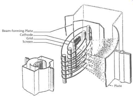
FIG. 7 Construction of beam tetrode (RCA)
As a small-signal amplifier stage the pentode offers a mixture of advantages and drawbacks. On the credit side, it gives a much higher stage gain (say 200) in an amplifier circuit of the type shown in FIG. 8, in comparison with that of the triode amplifier stage of the type shown in FIG. 4a, for which a gain of 50 would be typical. On the other hand the pentode tube gives a higher level of harmonic distortion than an equivalent triode circuit, and it has a somewhat higher noise level -- though this can still be very low in a well-designed tube -- than a triode because of the existence of partition noise in the pentode. This defect arises because the individual electrons which collectively make up the cathode current of the tube can arrive at either the anode or G2 in a random manner, and this means that even without an input signal the anode current will fluctuate about its mean level, an effect which is heard as noise.
With suitable amendments to the circuit to provide the necessary G2 voltage, the pentode can be used in any of the circuit layouts shown in FIGs 1 and 4, though unless a high stage gain is desirable a triode would be a more normal choice, if only because small-signal triodes, such as the ECC83 or the 6SN7, are very readily available as two tubes having closely similar characteristics within a single envelope, and this could save space on the chassis.
A final point to be considered in the use of a pentode amplifying tube is that the screen grid (G2) current is modulated by the input signal voltage on the control grid (G1) in exactly the same manner as the anode current. It has been seen that if G2 is connected to the anode then a pentode tube will behave as though it were a triode - with a much lower stage gain. What is not generally appreciated is that an almost identical behavior is given if G2 is fed from the +V supply line through a sufficiently high value load resistor that the screen and anode voltages move simultaneously in the same manner. Once again, the stage gain of the tube is reduced to the level of a triode stage.
Therefore, in order to obtain the full stage gain from a pentode amplifying tube, the circuit must be chosen with an adequate value of G2 decoupling capacitor (C4 in FIG. 8) to ensure that the G2 voltage remains at a constant level. On the other hand, it is possible to choose the values of the components associated with such an amplifier stage so that the gain will rolloff with frequency, either at the HF or LF ends of the frequency spectrum, where this gain reduction, and the phase changes associated with it, may help in stabilizing an amplifier using overall negative feedback.
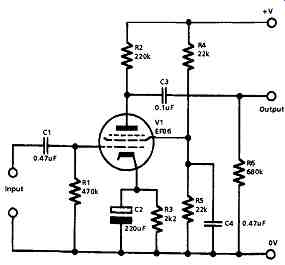
FIG. 8 Pentode gain stage Load Lines
If the tube manufacturers publish a full set of performance data it will be a straightforward matter to calculate the stage gain from the equation
Ao =IaR1/(R1 + Ra)
However, the necessary data are not always published, and in this case it is necessary either to use the Ia/V a data, if these are quoted, or to determine these for oneself. To do this it is necessary to have a fixed high voltage source, a variable low voltage (negative grid bias) source, a chosen value of load resistor, and a current meter. With this one can obtain the family of curved lines, relating anode current to anode potential for various grid bias voltages, shown in FIG. 9 -- those shown are published by Mullard Ltd for one half of an ECC83 double triode.
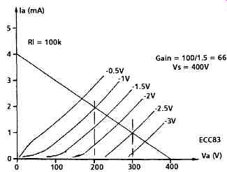
FIG. 9 ECC83 load lines
The two points on the I a and V a curves which can be defined are the anode voltage with no anode current - in this case I have chosen a supply voltage of +400V - and the anode current if the tube is turned fully on, which would be 400/100k (4mA) for a 100k anode load resistor. If a straight line is drawn between these two points the intercepts on the diagonal Ia/Vg curves will be at -1V and -2.5V corresponding to anode voltages of +200V and +300V. So, with this value of load resistor a change in anode voltage of 100V will be caused by a -1.5V change in the grid bias voltage. The gain of the stage (A~ for a stage without any added cathode circuit resistance, is therefore -100/1.5 = -66 (which is the calculated stage gain for an ECC83 tube with a 'p' value of 100 and an R a of 50k). The same graphical process can be carried out for other values of load resistor or other values of supply voltage.
Similarly, this graphical approach can be used to determine the stage gain of a pentode, as shown in FIG. 10. Here, the slope of the Ia/W" a curve is very much flatter than that of a triode - being almost parallel to the 0V axis - and this contributes to the higher stage gain of the tube, by comparison with a triode equivalent. However, the compression of the Ia/V a curves at more negative grid voltages indicates clearly that the high gain pentode amplifier tube gives a higher distortion level than the lower gain triode stage. It is also obvious from FIG. 10 that the mutual conductance (gm) of the EF86 pentode (the change in anode current for a fixed increment in grid voltage) increases towards the higher anode current end of the anode current graph, so for maximum stage gain for a given anode load resistor the tube should be operated at the highest value of anode current which is compatible with avoidance of signal waveform clipping on the negative peaks of anode current excursions.
 FIG. 10 Load lines for pentode gain stage
The triode cascode of FIG. 1 c -- there is little benefit in the additional complexity of a pentode tube as either V1A or V1B -- has similar gain characteristics to the pentode stage, with very much lower distortion. In this case, the simplest way of determining the stage gain is to determine the gm of the lower tube at the chosen anode voltage (gm = 1.25 for an ECC83, operating at Va = 100V, and Ia = 0.5mA), and then use the relationship Ao = gmR1 , so that an ECC83 cascode stage with a 100k anode load resistor would have a stage gain of 150, which is rather better than that given by the EF86. Since the voltage drop across the anode load will be 50V, a supply voltage of, say, +220V would be quite adequate, and would allow an output voltage swing approaching 100Vp-p. For a higher output voltage swing, a larger value of anode load resistor and a higher +V supply line voltage would be required.
===
