AMAZON multi-meters discounts AMAZON oscilloscope discounts
LEARNING OBJECTIVES:
Upon completion of this Section on the imaging of doubled-sided pc boards, the student should be able to:
1. Know the processes involved in double-sided imaging.
2. Chemically and mechanically clean pc boards.
3. Be familiar with dry-film photo-resists.
4. Use the laminator to apply dry-film resist to pc boards.
5. Properly register the diazo phototools onto both sides of a pc board.
6. Expose dry-film photo-resist.
7. Use a radiometer to monitor exposure time.
8. Prepare developing solution and spray-develop pc boards.
9. Inspect and touch up any defects in developed pc boards.
0. INTRODUCTION
In Section 17, the first of many phases in the processing of double-sided plated-through-hole pc boards was discussed. The panels to be processed were stacked and pinned together and all the holes were drilled with an automatic multispindle CNC machine. After drilling, the panels were unpinned, mechanically deburred, and then processed through cleaning and drying. They were then vertically racked in specially designed stainless steel racks and processed through a 16-bath electroless copper deposition line which plated approximately 25 u-inches of pure copper on all board surfaces including the edges and the walls of the drilled holes. To ensure a continuous copper surface without voids, especially on the hole walls, the boards were finally passed through a flash-plating process which electroplated an additional 100 pinches of copper onto all surfaces.
With the boards plated with approximately 125 u-inches of copper, the next step in their processing is dry-film photo-resist imaging. The boards are first mechanically cleaned and then chemically treated to activate the flash plated copper. Both sides of the boards are then laminated with a light-sensitive dry-film photo-resist. The light-sensitive surfaces are exposed through positive-working phototools of the conductor patterns (see Section 16). These images are next developed, which exposes just the copper patterns of conductors and terminal pads of the artworks. These patterns, as well as hole walls, will subsequently be electroplated with copper and then 60/40 tin-lead solder (Section 19).
Recall that in the print-and-etch technique for processing single-sided boards (Section 13), the photo-resist employed was a light-sensitive liquid. Al though this photo-resist is suitable for simple prototype work, it does not lend itself to plated-through-hole applications and thus has been superseded by the newer dry-film types. There are two reasons for this. First, the solvent-type developers required to process liquid resists is becoming increasingly more difficult to dispose of properly because of environmental considerations. Second, it is difficult to accurately control the thickness of liquid resists, resulting in lower yields of flaw-free boards. Both of these problems are overcome with the use of dry-film photo-resists. Uniform thickness results in more predictable exposure time and little, if any, pinhole touch-up is requited. Dry-film resists that can be developed and stripped in aqueous-based chemicals are also available. These resists can be applied simultaneously to both sides of a double-sided board, lending themselves ideally to this application. In addition, dry-film resists can more easily withstand almost any electroplating bath solution and, as a result, allow the application of copper from a copper sulfate bath as well as 60/40 tin-lead solder from a fluoborate bath. In this Section we describe the imaging process using only dry-film photoresists.
1. PROCESSES INVOLVED IN DOUBLE-SIDED IMAGING
The basic steps required to image a double-sided pc board are shown in the flow chart of FIG. 1. The flow chart is accompanied by illustrations which show the results of the sequential steps described in the imaging process. Subsequent sections of this Section detail each of these steps.

FIG. 1 Basic flow chart with pictorial sequence of the imaging process.
The imaging process begins with boards that have been drilled, deposited with electroless copper, and flash-plated (Section 17). Both sides of these panels are then chemically and mechanically prepared to accept a uniform lamination coating of dry-film photo-resist. With the resist laminated on both sides, it is exposed with two diazo phototools (Section 16), one for the component side and one for the circuit side. Phototool alignment will be accomplished using the underlying hole pattern on the board. Recall that diazo phototools show the conductor pattern images as translucent (amber), which aids in this alignment. Also, the amber pattern is opaque to ultraviolet light, which is used to expose the resist. The translucent quality of the diazo film allows each pattern to be registered in perfect alignment with the drilled holes on either side of the board due to the fact that they are clearly visible through the amber pattern. This eliminates the need for any special registration pinning arrangement between the two phototools.
After exposure through the two diazo phototools, the board is developed to produce an image such as that shown in FIG. 1. Note that after developing, the resist is removed from only the conductor pattern, terminal pads, and holes. These will all be copper- and solder-electroplated. All the copper that is to be removed remains covered with the photo-resist.
2. COPPER CLEANING FOR DRY-FILM APPLICATION

FIG. 2 Chemical and mechanical cleaning procedure for bulk pc board
stock prior to resist application.
Optimum thy-film resist adhesion is accomplished only if the copper surface is properly cleaned. The cleaning cycle outlined in FIG. 2 will produce copper surfaces that are completely degreased, slightly acidic, and thoroughly dry. Careful attention to this cleaning cycle cannot be emphasized enough. Most problems that develop in subsequent processing steps can often be directly attributed to improper cleaning.
First, an acid dip is required to leave the copper surface in a slightly acid state to improve resist adhesion. The acid dip uses CP (chemically pure) or re agent-grade sulfuric acid. One part of acid is slowly added to 9 parts of cold tap water. This mixture will yield a 10% by volume acid dip solution. (Caution: Never add water to acid. This causes violent eruptions to occur.) The container used for the dip tank can be of Pyrex or an acid-resistant plastic such as poly ethylene or polypropylene. Plastic gloves should be worn whenever handling acid solutions. The pc board is dipped into the acid solution for approximately 2 minutes while gently rocking the container ( FIG. 3a). The pc board is then removed from the acid dip and completely rinsed on both sides for at least 30 seconds.
Cleaning of the copper surfaces is best accomplished with a mechanical scrubber, such as that shown in FIG. 3b. This scrubber consists chiefly of a series of motor-driven hard-rubber rollers positioned horizontally along the length of the unit. Panels to be cleaned are placed on these rollers and are trans ported into the unit at a speed of approximately 4 to 5 feet per minute. Inside the unit and above the rollers is a cylindrical scrubbing brush (320 grit) which rotates in a direction counter to that of board travel. The vertical position of the brush is adjusted by a small handwheel located at the top right side of the ma chine. After the boards enter the scrubber, water flows over their surface as they pass under the brush. The copper surface (one side only) is thus mechanically cleaned of grease, oils, and foreign particles. The small flow of water on both the board and the brush acts as a coolant and also flushes away contaminants. As the board moves from under the brush, it is sprayed with water to further aid in removing foreign matter. It finally passes between a series of air knives (parallel air tubes having a narrow slit along their lengths) which direct streams of high-pressure air over both surfaces of the board simultaneously to promote drying. Because the scrubber described cleans only one side of a board at a time, a double-sided board must be turned over and run through a second time. Larger and more elaborate scrubbers are available that will clean, rinse, and dry both sides of pc boards simultaneously.
The cleaned board is then placed vertically into a forced-air oven for approximately 15 minutes at a temperature of 150°F (66°C). This prebake cycle just prior to resist application accomplishes two functions: (1) the elevated temperature will remove any moisture from the board, which would adversely affect resist adhesion, and (2) by raising the temperature of the copper surfaces to 150°F, improved resist adhesion results. Timing and temperature in this heating phase are somewhat critical. Prolonged exposure to heat will result in. surface oxides to be re-deposited onto the copper surfaces. Although dry-film resist can be applied successfully over a light oxide film, this should be avoided. In addition, increasing the oven temperature to shorten the prebake cycle should also be avoided, since higher temperatures do not improve resist adhesion and can degrade the copper bond. After this prebake cycle, the board is ready for dry-film resist application.
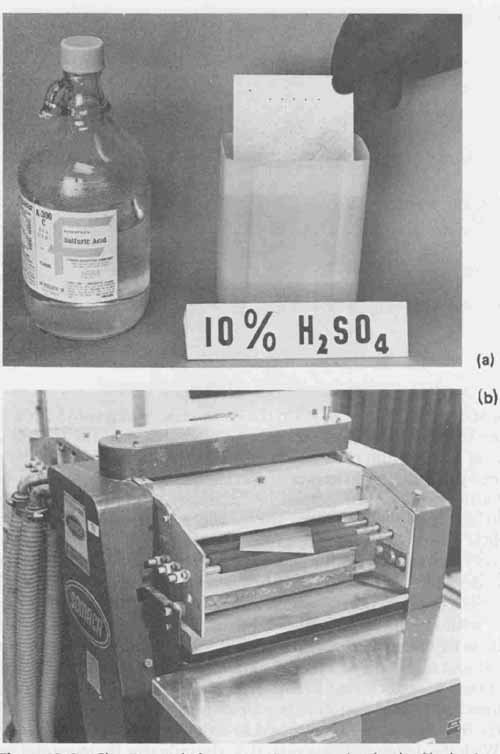
FIG. 3 Cleaning cycle for copper in preparation for dry-film lamination:
(a) chemical cleaning by an acid dip; (b) Somaca scrubber used to mechanically
clean copper.
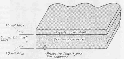
FIG. 4 Composition of dry-film resist.
3. DRY-FILM PHOTO-RESIST
The use of dry-film photo-resists in the manufacture of printed circuit boards is a process that has been used extensively since the early 1970s. A typicalcom position of the dry-film resist is shown in FIG. 4. The resist is a light-sensitive photo-polymer, dry in nature and available in thicknesses of from 0.5 to 2.5 mils. Widths range from 3 to 25 inches that are available on continuous rolls of 100, 250, and 400 feet. The resist is sandwiched between two layers of plastic. One side is protected with a polyester cover sheet and the other side is covered with a polyethylene separator sheet. These plastic sheets are intended to protect the dry film from handling damage and also to provide a gastight seal against the oxygen in the air, which would quickly degrade the film.
As with any other light-sensitive resist, correct handling is crucial. Be cause these dry films are sensitive to light in the ultraviolet range, they should be stored and used only in an area illuminated with gold fluorescent tubes or lighting that does not emit ultraviolet light. Dry films are also sensitive to extreme heat and should therefore be stored at temperatures below 70°F (21° C).
Dry-film resists are categorized as either solvent- or aqueous-developing types. With the demands being placed on the industry for more and better environmental controls, the aqueous types are being used more extensively. Although dry-film resists are available from several manufacturers, all are similar in makeup and also in the fabrication processes required. For our purposes, we have elected to use Laminar AX, which is an aqueous-developing dry film, blue in color, manufactured by the Dynachem Corporation of California. This resist will withstand both the copper sulfate and the tin—lead fluoborate plating solutions which will be used in the pattern-plating phase of processing described in Section 19. The optimum size of resist selected for our purposes is a thickness of 2 mils and a width of 8 inches, which will cover the bulk stock described in this Section.
4. DRY-FILM LAMINATOR
Dry-film photo-resists are applied to the clean and slightly acidic copper surfaces with a laminator. A typical laminator capable of processing boards up to 12 inches wide is shown in FIG. 5. This laminator applies the dry film simultaneously to both sides of the pc board. Dry-film resists are applied under pres sure at elevated temperatures with a specific feed-through rate.
A typical laminator consists of (1) a pair of hard-rubber pressure rollers, (2) a pair of take-up rollers, (3) a pair of heat shoes, (4) a pair of temperature sensors for each shoe, (5) a variable-pressure adjustment control, and (6) a van able-motor-speed control to adjust the feed rate of the dry film.
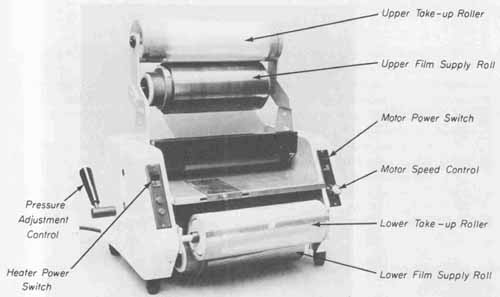
FIG. 5 Prototype laminator for dry-film photo-resist application.
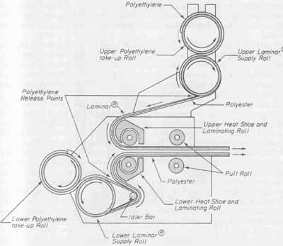
FIG. 6 Typical threading diagram for laminator.
Dry-film threading of the laminator for double-sided pc boards is shown in FIG. 6. Two rolls of dry film, one for each side of the pc board, are used. The protective polyethylene separator sheets are removed from both rolls of dry film and fed into both the upper and lower take-up rollers. The upper and lower rolls of dry film are fed between the hard-rubber rollers with exposed dry film in contact with each other. The opposite sides of both rolls of film, together with the polyester cover sheets, are in contact with both heat shoes. As the pc boards are fed between the rolls of dry film, the take-up rollers remove, on a continuous basis, the polyethylene separator sheets just prior to the film contacting the pc board. The film is heated as it passes over the heat shoes and is laminated onto the copper surfaces by the pressure of the hard-rubber rollers as the pc board moves through the laminator.
Successful application of Dynachem Laminar AX to prepared copper surfaces requires the following laminator specifications: (1) upper and lower heat shoe temperatures set to 235 ± 10°F, (2) laminating feed rate of approximately 5 linear feet per minute, and (3) moderate pressure setting of the hard-rubber rollers. With the laminator’s parameters correctly set, the application of the dry-film photo-resist onto the pc board can now be performed.
5. DRY-FILM PHOTO-RESIST APPLICATION
In Sec. 2, the pc board was placed into an acid dip, machine scrubbed and dried, and prebaked in an oven. These heated boards should be laminated immediately upon removal from the oven. Cold boards would act as heat sinks and remove heat from the dry film, resulting in poor resist adhesion. For this reason, the oven should be placed close to the laminator so that no delay will result between removing the board from the oven and placing it into the laminator.
With the laminator controls set to the settings specified in Sec. 4 and allowing the laminator time to reach the preset temperatures, approximately 1 foot of dry film is run through the laminator. This is a precautionary measure that should be done any time a heated laminator has remained idle for any length of time. The reason for doing this is that the first foot of film on the rolls has been in close contact with the heat generated by the heat shoes of the laminator and, as a result, has been degraded by the long exposure to elevated temperatures. Film damaged from excessive heat results in heat fog. A pc board processed with heat-fogged film will not process successfully in the subsequent steps.
After the one foot of film has passed through the laminator and with the film feed still on, the board is removed from the oven (held by the edges only) and fed immediately into the laminator by pushing it gently up to the moving rollers. The board contacting the rollers will be pulled into the laminator, where heated dry-film resist will be applied simultaneously to both sides of the copper surface. This process is shown in FIG. 7a.
As the board with the applied resist leaves the laminator, it is removed by cutting off the film either with the aid of the slide cutter mounted at the rear of the laminator or with a single-edge razor blade (Fig. 7b). Efficient laminating can be realized if two people operate the unit: one person feeding the boards into the laminator while the other cuts and removes the processed boards.
A laminated double-sided pc board is shown in FIG. 8. The board is sandwiched between two layers of dry film, each protected by a polyester cover sheet. After the board has been laminated, it is extremely important not to disturb or remove the polyester cover sheets (even at the corners). These sheets serve as “gas seals,” preventing oxygen in the atmosphere from contacting the underlying resist film and causing it to polymerize (i.e., change it chemically into heavier molecules). The excess film is carefully trimmed as close as possible to the board edges, using a sharp razor blade. This technique is shown in FIG. 9.
The temperature of the laminator must be carefully maintained at 235 ± 10°F. At elevated temperatures, resist blistering occurs, and at temperatures lower than the specified range, a breakdown in resist adhesion to the copper surface can result. If the laminator is in continuous use, careful monitoring of the two thermometers is essential to minimize problems.
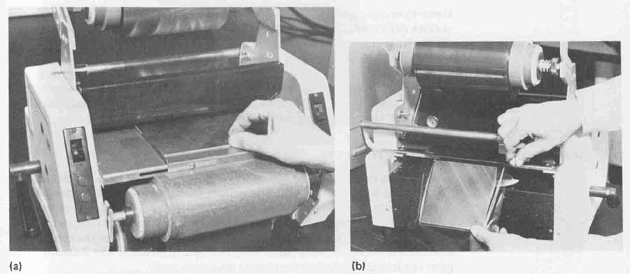
FIG. 7 Dry-film laminating technique: (a) pc board fed into laminator;
(b) laminated pc board removed using rear film cutter.
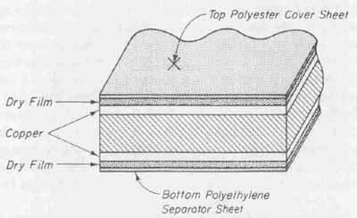
FIG. 8 Laminated double-sided pc board.
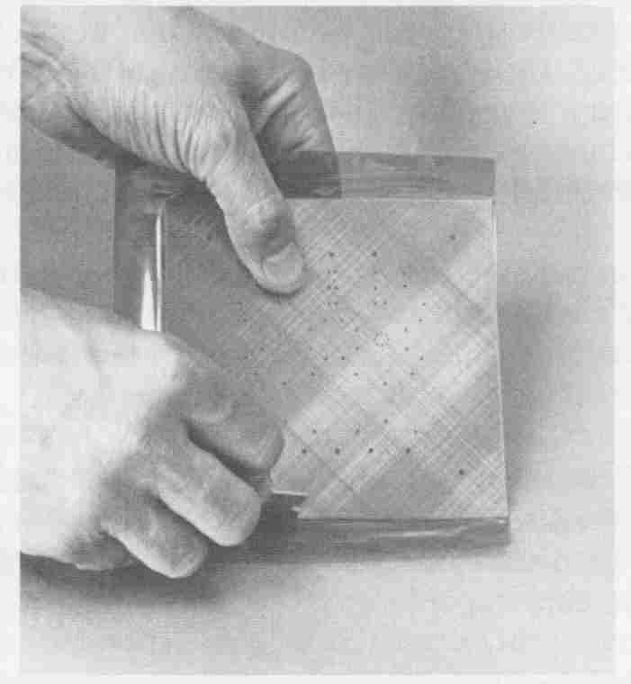
FIG. 9 Trimming excess dry film from edges of laminated pc board.
After laminating, a normalizing period of 30 minutes before exposure is recommended by the manufacturer. This 30-minute period allows the board and dry film to return to room temperature, resulting in an improvement of the adhesion properties of the film. Because the film is extremely sensitive to ultra violet light, the normalizing interval must be in a gold-light area.
(cont. >>) .