A shift register consists of a number of flip-flops connected together in such a way that the circuit can store a digital word for a time, and then can transfer it to another circuit on demand.
EIGHT-BIT SHIFT REGISTER
Fig. 5-1 shows an 8-bit shift register that uses Set-Reset master-slave flip-flops. It accepts serial data and is driven by the clock pulse. The register shown is circuit type 5491/ 7491.
When inputs A = B = 1, Gate 1 = 0 and Gate 2 = 1. These conditions put a 0 on the Reset ( R) input and a 1 on the Set (S) input to flip-flop 1. When CP goes high, it puts a 0 on the CP inputs of the flip-flops. Since S = 1, this causes flip-flop 1 to go to the Q = 1 state. At the same time, the R and S inputs to the flip-flop are disabled. When the clock goes low, the CP input to the flip-flop goes high. This locks the flip-flop in the Q = 1 state and frees the S and R inputs to go to the next condition called for by inputs A and B. Assume inputs A and B stay high. As a result of the first clock pulse, flip-flop 2 has its S input = 1 and its R input = 0. On the next clock pulse, therefore, flip-flop 2 will be driven to the Q = 1 position. At the same time, flip-flop 1 will remain in the Q = 1 state.
Before the next clock pulse arrives, let A or B (or both) go to 0. This sets the R input of flip-flop 1 to a 1 and the S input ...
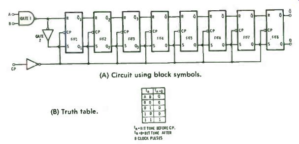
(B) Truth table.
(A) Circuit using block symbols.
Fig. 5-1. Eight-bit shift register.
... to a 0. Flip-flop 2 has Q = 1, which puts a 1 on the S input of flip-flop 3. The next clock pulse will, therefore, drive flip-flop 3 to the Q = 1 state; flip-flop 2 will stay in the Q = 1 state; and flip-flop 1 will be driven to the Q = 0 state.
If A and B are both set to 1 again, the next clock pulse will drive output Q of flip-flop 1 to 1, flip-flop 2 to 0, flip-flop 3 to 1, and flip-flop 4 to 1. After the eighth clock pulse, the first bit of data that entered the register will appear at the output of the eighth flip-flop. The process is summarized in the truth table, where t_ + 8 means the time slot after the eighth clock pulse.
If we want to put in a specific 8-bit word, we need only change the input bit as required before each clock pulse.
To extract a word stored in the register, 8 clock pulses must be applied; the word will appear at the output in serial form.
At the same time one word is being extracted, a different word can be loaded in. Alternatively, the register can be set to all 0s by setting B = 0 and clocking 8 times (or set to all is by setting A = B = 1 and clocking 8 times). One input, for example B, can be used as a control. Whenever B = 1, the circuit will follow A, entering a 0 if A = 0 and entering a 1 if A = 1.
Fig. 5-2 shows how the type 5491/7491 can be operated in tandem
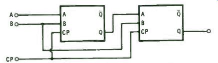
Fig. 5-2. Using two ICs in tandem operation.
Suppose you are working with a 16-bit word instead of an 8-bit word and need a serial-in/serial-out shift register. Fig. to handle a 16-bit word. Longer word lengths can be handled by adding more units, connecting output Q to the next A input, and paralleling input B and the CP.
SERIAL-PARALLEL SHIFT REGISTER
Data can exist in both serial and parallel format, and changes from one form to the other are necessary. The shift register shown in Fig. 5-3 uses 5 master-slave type flip-flops and can convert data from serial operation to parallel operation and vice versa.
Master-slave flip-flops give top priority to their Clear and/or Preset inputs. In the circuits used in the 5496/7496 IC, the Clear input has priority over the serial input (DE), but not over Preset. When Clear is set to 0, all the outputs (Q A through Q E) are driven to 0. When Preset is set to 1, the NAND gate associated with each flip-flop is free to follow its other input (P A through P E). Thus, if Preset Enable = P A = 1, the output of Gate 1 = 0 and causes flip-flop A and output Q to go to 1. If input P A = 0, however, Gate 1 = 1 and output Q A is not affected. The other parallel inputs act in the same manner as input P A. For serial-in/serial-out operation, Preset Enable is set to 0 and Clear to 1. The circuit then operates like the previously considered register, type 5491/7491. The only difference between the two is that the data does not enter via a 2-input NAND gate but via a 1-input inverter. The data is transferred on the leading edge of a positive-going clock pulse. This means that the input data must be present at Dg ( Fig. 5-3) before the circuit is pulsed, or else the data will not be entered in flip-flop A. Flip-flop B, however, is fed by flip-flop A, and thus data is always present at its input. Similarly, data is present at the input of flip-flops C, D, and E. Since the outputs of the internal flip-flops are brought out side the package, the data entering serially at Dg is available in parallel form at outputs Q A through Q E. Thus, by using these outputs, the device will work as a serial-to-parallel converter.
Note, however, that when a word is entered serially, the first bit to enter appears first at Q A, then at Q B, and finally at Q E after the fifth clock pulse. In other words, the serial-to-parallel conversion is not complete until after the fifth clock pulse (parallel outputs prior to the fifth pulse will not be correct con versions). If the parallel outputs are being used to drive indicator circuits, the intermediate words may be acceptable. But if the parallel outputs are being fed to computing circuits, some...
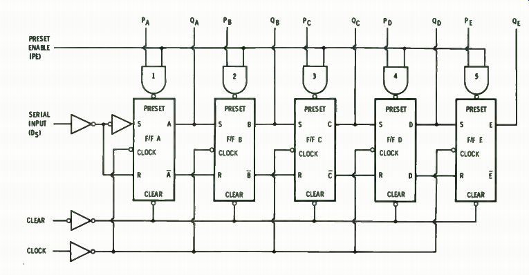
Fig. 5-3. Block diagram of a serial-parallel shift register.
... form of output blanking or other control scheme may be necessary.
For parallel-to-serial conversion, data is applied to the P inputs. For example, when Preset Enable goes to 1, and PA = 1, Gate 1 goes low. This is the activating signal for flip-flop A, and QA goes high. However, as mentioned above, if PA = 0 when PE = 1, Gate 1 remains at 1 and the flip-flop is not affected; the output could be 1 or 0. To set in a parallel word consisting of both is and Os, set Clear to 0 and PE to 1. Since PE has priority over Clear, all parallel inputs that are 1 will set their corresponding flip-flops to 1, while the Clear = 0 input will drive all the others to 0. To prevent driving all the flip-flops to 0, the Clear = 0 signal must be removed prior to or simultaneously with PE = 1. The word is then taken out serially by applying is or Os to D8 and clocking the register. Note that the register can be set to all Os, by keeping Ds = 0, while a word is being clocked out.
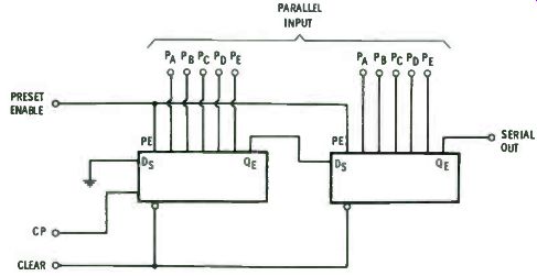
Fig. 5- 4 Shift registers connected for tandem operation.
Registers can be combined to handle words longer than 5 bits, as shown in Fig. 5-4.
LEFT-SHIFT AND RIGHT-SHIFT REGISTERS
For shift registers discussed thus far, data has been entered at the left side-that is, at the left side of the schematic or drawing-and has then been shifted to the right ( or, entered at the top and removed from the bottom). In any case, the data could not be moved forward and then backward, like maneuvering soldiers in ranks or boxcars on a railroad track. In some logical operations, a reverse or left-shift maneuver is needed.
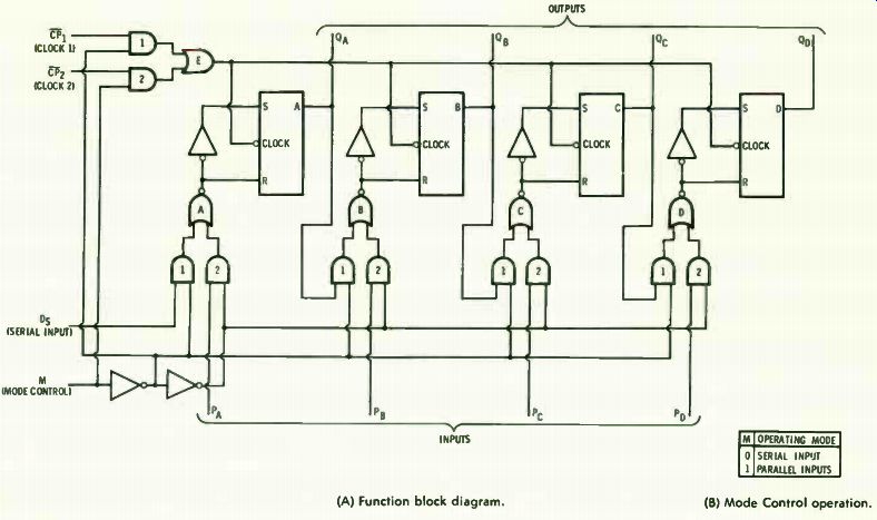
Fig. 5-5. Left- or right-shift register. (A) Function block diagram. (B) Mode
Control operation.
The shift register in Fig. 5-5A (type 5495A/7495A) can handle data in a serial or parallel form and can shift it left or right as required. The circuit is similar to previous registers but also has a Mode Control network that determines operation. Let the Mode Control input (M) be 0 ( Fig. 5-5B). This causes all the AND gates marked 2 to have one input 0 and the gates are closed or inhibited-parallel inputs PA through PI , cannot get into the register.
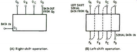
(A) Right- shift operation. ( B) Left- shift operation.
Fig. 5-6. Operational method of Fig. 5-5.
The gates marked 1, however, all have a 1 input from the Mode Control circuit, so they are not inhibited. Data applied at the Serial input terminal will be fed into the register with each clock pulse. If the data at Ds is a 1, then Gate 1 = 1, Gate A = 0, and the inputs of the A flip-flop are S = 1, R = ; if D8 = 0, S = 0 and R = 1. The data enters the register when the circuit is clocked by CPI. The flip-flops are the same master slave Set-Reset type used in the registers discussed previously.
Data is entered on the negative edge of the clock pulse. Since the clock input circuit does not provide inversion, a negative going clock signal is required. If a positive clock pulse is used, ...
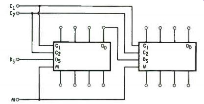
Fig. 5-7. Registers connected to provide
expanded output.
... the data will be entered on the trailing edge of the pulse. Since the data in each flip-flop is available at output pins, the circuit functions as a right-shift register and/or as a serial-to-parallel converter ( Fig. 5-6A) . When the Mode Control is 1 ( Fig. 5-5B), the " 1" gates are inhibited and the "2" gates are enabled. Data applied at the serial input is blocked, but data applied at the parallel inputs (P A through P.) will enter the register whenever Clock 2 goes low. If data is taken out at outputs Q A through Q D, the register acts as a temporary store or memory. To obtain left-shift operation, serial data is fed into P D ( M = 1). Output Q D is then applied to input Pc; output Qc is applied to input PE; output Q. is applied to input PA; and the output from Q A is left-shifted data ( Fig. 5-6B) . If left-shift and right-shift are to be obtained from the same clocking source, then clock inputs 1 and 2 can be tied together without affecting circuit operation.
Data has to be shifted left or right only as many places as required. This characteristic is useful in mathematical operations. Words longer than 5-bits can be handled as indicated in Fig. 5-7.
Prev: Link | --Link | --Link | --MULTIPLEXERS
Next: COUNTERS
Guide Index : Transistor-Transistor Logic (early 1970s)