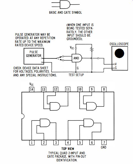
Fig. 4-1. Checking the operation.
| Home | Audio mag. | Stereo Review mag. | High Fidelity mag. | AE/AA mag. |
4-1. To Check the Operation of an AND Gate
Equipment: Pulse generator or square-wave generator, battery.
Connections Required: Connect scope at output of AND gate.
Connect output from generator in turn to each of the inputs of the AND gate. Finally, connect the output from the generator to all of the inputs of the AND gate. Use rated Vee supply voltage.
Fig. 4-1. Checking the operation.
Procedure: Apply a suitable output level from the generator, such as 2.5 volts peak. Observe the scope screen as the foregoing test connections are made. (See diagram in Fig. 4-1 .) Evaluation of Results: An output pulse should be displayed on the scope screen only when the generator is connected to all of the AND gate inputs. Otherwise, the gate is defective and should be replaced. (In a noisy environment, a gate may appear to be defective, although it is actually normal, unless the unused gate inputs are grounded to "kill" noise-voltage pickup.)
NOTE 4-1 NAND Gate Characteristics
A NAND gate is checked in the same manner as an AND gate. The only distinction is that a NAND gate inverts the polarity of the output pulse with respect to the input pulses. Note that an AND gate or a NAND gate has a minimum of two input terminals; however. these gates may have any maximum number of input terminals. For example. B-input AND, and NAND gates are often encountered (Fig. 4-2). However. the operating principle remains the same, regardless of the number of inputs.
For example, if an AND gate has 8 inputs, an output pulse will normally be obtained only when all eight inputs are simultaneously driven logic high. Always check the manufacturer's data for correct voltages and polarities. Note also that gates are generally fabricated with several gates included in a single IC package. Thus, a quad 2-input AND gate is an IC package that contains four AND gates, each with two inputs.
4-2. To Check AND Gate Action in a Scanner-Monitor Receiver
Equipment: None of an AND gate.
Connections Required: With reference to Fig. 4-3 , connect scope via lo-C probe at the clock output, FF1 Q output, FF1 Q output, FF2 Q output, and FF2 Q output, in turn.
Procedure: Observe the waveform displayed (or absence of waveform) at each of the test points.
Evaluation of Results: A square-wave train (clock pulses) are normally present at the clock output; half-frequency square waves in opposite polarities are normally present at the FF1 Q and the FF1 Q outputs; quarter-frequency square waves in opposite polarities are normally present at the FF2 Q and the FF2 Q outputs. Incorrect output, or absence of output, at a
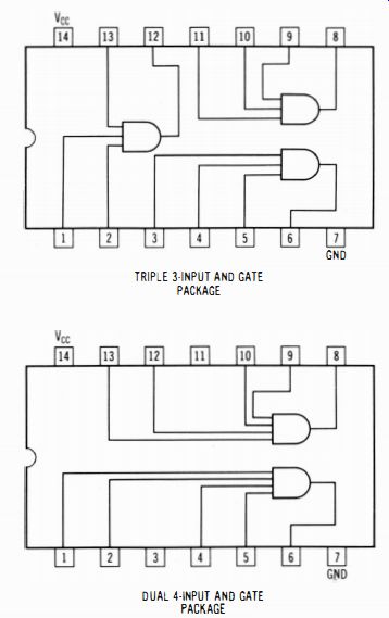
Fig. 4-2. Typical digital waveform in TTL circuitry, showing High (1) and
Low (2) thresholds. (CMOS circuitry employs supply voltages in the range from
3 to 18 volts; check manufacturer's data sheet). test terminal indicates a
fault in the associated device. The array of square waves depicted in the diagram
comprises the specified timing diagram for the digital system.
(B) Normal operating waveforms.
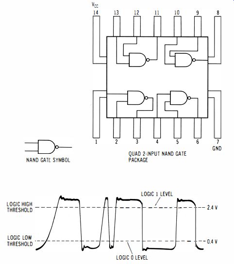
Fig. 4-3. Simplified block diagram for a 4-channel digital-logic section in
a scanner-monitor radio receiver.
NOTE 4-2 Digital Clock Function
A clock is a free-running multivibrator which functions to synchronize circuit actions throughout a digital system. A flip-flop (FF) is a bistable multivibrator; when the FF is "on," its Q output is logic-high-when "off," its Q (NOT Q) is logic-low. The logic-high state is symbolized by 1, and the logic-low state is symbolized by O. When the Q output of a FF is 1, its Q output is 0, and vice versa. The Q and Q outputs are said to be complementary. Each AND gate has a 0 output unless both of its inputs are simultaneously 1. If both AND gate inputs are 0, its output is 0; if the AND gate inputs are 1,0 or 0,1 , its output is 0. Note that the timing diagram in Fig. 4-3 represents a positive operating level, with positive logic. However, the technician will encounter instances of positive operating level with negative logic, of negative operating level with negative logic, and of negative operating level with positive logic, as exemplified in the diagram of Fig. 4-4.
(A) Positive operating level, with positive logic .
(B) Positive operating level, with negative logic .
(C) Negative operating level, with negative logic.
(D) Negative operating level, with positive logic.
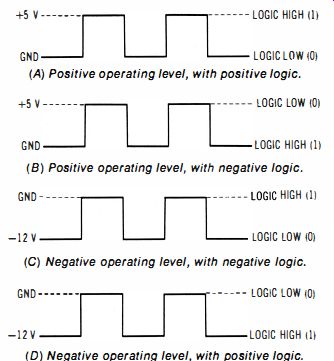
Fig. 4-4. Basic example of positive and negative operating levels, with positive
and negative logic conventions.
4-3. To Check the Operation of an OR Gate.
Equipment: Pulse generator or square-wave generator, and battery.
Connections Required: Connect scope at output of OR gate.
(A) Test setup.
(B) Basic OR gate symbol.
Vee (c) Typical triple 3-input OR gate package.
(D) NOR gate symbol.
(E) Typical triple 3-input NOR gate package.
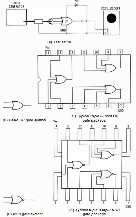
Fig. 4-5. Checking the operation of an OR gate.
Connect output from generator in turn to each of the inputs of the OR gate. Finally, connect the output from the generator to all of the inputs of the OR gate. Use rated Vee supply voltage.
Procedure: Apply a suitable output level from the generator, such as 2.5 volts peak. Observe the scope screen as the foregoing test connections are made. (See Fig. 4-5.)
Evaluation of Results: An output pulse should be displayed on the scope screen whenever the generator output is applied to one or more of the OR gate inputs. Otherwise, the gate is defective and should be replaced.
NOTE 4-3 NOR Gate Characteristics
A NOR gate is checked in the same manner as an OR gate. The only distinction is that a NOR gate inverts the polarity of the output pulse with respect to the input pulse(s). Note that an OR gate or a NOR gate has a minimum of two input terminals; however, these gates may have any maximum number of input terminals. The operating principle remains the same, regardless of the number of inputs. For example, if an OR gate has five inputs, an output pulse will normally be obtained whenever any input terminal, or any combination of input terminals, is driven logic-high. Always check the manufacturer's data for correct voltages and polarities.
4-4. To Check the Operation of an XOR Gate
Equipment: Pulse generator or square-wave generator, and battery.
Connections Required: Connect scope at output of XOR gate.
Connect output from generator in turn to each of the inputs of the XOR gate. Finally, connect the output from the generator to both of the inputs of the XOR gate (Fig. 4-6) . Use rated Vcc supply voltage.
Procedure: Apply a suitable output level from the generator.
Observe the scope screen as the foregoing test connections are made.
Evaluation of Results: An output pulse should be displayed on the scope screen whenever the generator output is applied to one of the XOR gate inputs. On the other hand, no output pulse should be displayed when the generator output is applied simultaneously to both of the XOR gate inputs. Fai lure to respond normally to these tests indicates that the XOR gate is defective.
NOTE 4-4 XOR Gate Characteristics
An EXCLUSIVE OR (XOR) gate has two inputs; it produces a logic high output only when its inputs are driven to opposite levels. If its inputs are 1, 1 or 0,0, the XOR gate produces no output (is at a logic-low level). An EXCLUSIVE NOR (xor) gate is checked in the same manner as an XOR gate. The only distinction is that an XOR gate inverts the output that would be obtained with an XOR gate. In other words, an XOR gate produces a logic-low output only when its inputs are driven ...
(A) Test setup.
(B) Basic XOR gate symbol.
(C) Typical quad 2-input XOR gate package.
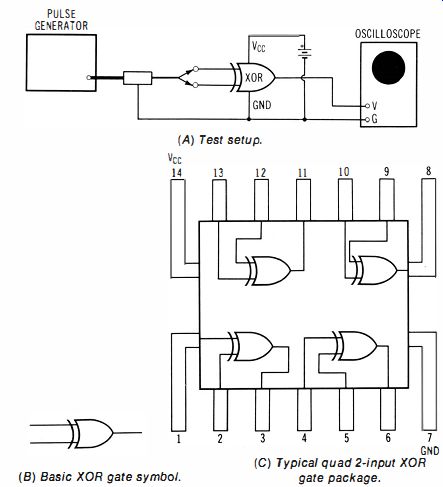
Fig. 4-6. Checking the operation of an XOR gate.
... to opposite levels. If the XOR inputs are 1,1 or 0,0, the gate output is at a logic-high level. The normal responses of AND, OR, NAND, NOR, XOR, and XOR (XNOR) gates are summarized to good advantage by means of truth tables as shown in Fig. 4-7.
4-5. To Check the Operation of an AND-OR-INVERT Gate
Equipment: Pulse or square-wave generator, and battery.
Connections Required: With reference to Fig. 4-8, connect output terminal of device to vertical-input channel of scope.
Connect output from generator to AND gate inputs, as explained next. Connect rated Vee supply voltage from Vee terminal to ground.
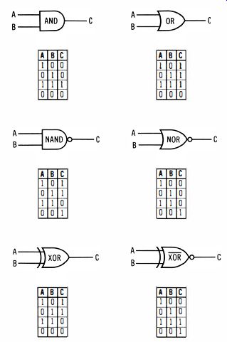
Fig. 4-7. Truth tables summarize normal responses.
Procedure: Use an appropriate output level from the squarewave generator at any repetition rate within the specified range of the device. Apply the test signal in turn to each individual AND-gate input terminal, and observe scope screen.
Then, apply the test signal in turn to each set of AND-gate input terminals, and observe scope screen.
Evaluation of Results: In normal operation, no waveform will be displayed on the scope screen unless the test signal is applied simultaneously to a set of AND-gate input terminals.
Otherwise, the device is defective and should be replaced .
4-6. To Check the Operation of a Full Adder
Equipment: Pulse generator or square-wave generator, and battery.
(A) Typical package pin-out and test setup.
(B) Basic four-wide 2-2-2-3 input AND-DR-INVERT gate symbol.
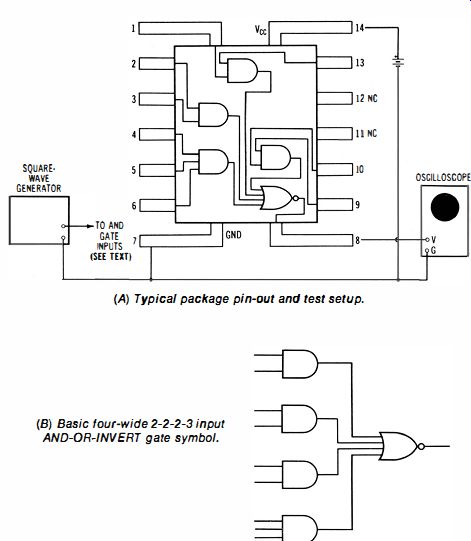
Fig. 4-8. Test of AND-OR-INVERT gate operation.
Connections Required: As shown in Fig. 4-9, connect a dual trace scope at the Carry and Sum outputs of the full adder.
Connect output from generator to one, two, or three inputs of the full adder, as successively listed in the truth table.
Use rated Vee supply voltage.
Procedure: Apply a suitable output level from the generator.
Observe the scope screen as the foregoing test connections are made.
Evaluation of Results: An output pulse is normally displayed on channel A, on channel B, or both, when corresponding A, B, and C' pulses are applied to the full adder. Failure to respond in accordance with the truth table indicates that the full adder is defective.
NOTE 4-5 Full Adder Operation
A full adder consists of two half adders with an OR gate. A half adder (Fig. 4-10) consists of an XOR gate and an AND gate (or equivalent PULSE GENERATOR arrangement).
(B) Basic full adder symbol.
(C) Typical package pin-out. NC = No connection
(d) Truth table.
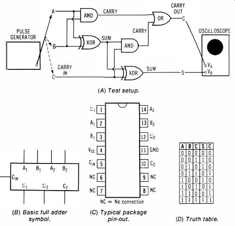
Fig. 4-9. Check of full adder operation.
A half adder has two inputs and a sum (S or Sigma) output and a carry (C) output. A full adder has two inputs and a carry-in (C') input, with a sum output and a carry-out output. The inputs are customarily designated A and 8; pulses applied to the inputs are logic-high or logic-low levels and are cal led binary digits (bits). The foregoing adders are two-bit devices, since they have two inputs. Observe that the truth table for an adder is basically a statement of the rules for binary addition.
(A) Gate arrangement.
(B) Truth table.
(c) Operating waveforms.
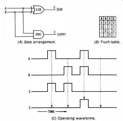
Fig. 4-10. Half adder.
4-7. To Check the Operation of a 4-Bit Latch
Equipment: Two square-wave generators, and battery.
Connections Required: As shown in Fi g. 4-11, connect the out
put from one square-wave generator to the clock input of a selected latch, and connect the output from the other squarewave generator to the data input of the latch. Connect the A channel of a dual-trace scope to the Q output of the latch, and connect the data input of the latch to the B channel of the scope. If the square-wave generators have sync facilities, lock generator 2 from the output of generator 1. Use rated Vee supply voltage.
(A) Test setup.
(b) Truth table.
(c) Typical dual 4-bit latch package.
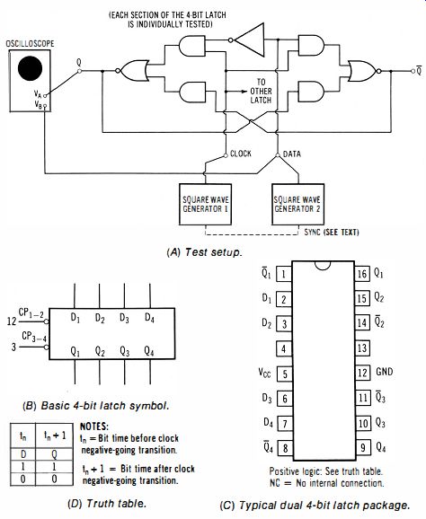
Fig. 4-11. Check of 4-bit latch operation.
Procedure: Operate the clock generator at two or three times the repetition rate of the data generator. Observe the Q output waveform with respect to the data input waveform.
Evaluation of Results: As indicated by the truth table, the Q out· put waveform normally reproduces the data input waveform, but lags by one-half of a clock cycle. Thus, if the clock generator is operating at twice the rate of the data generator, and the generators are synchronized, the Q output waveform normally lags the data input waveform by one-quarter cycle.
Otherwise, the latch is defective and should be replaced.
NOTE 4-6 Latch Characteristics
A latch is basically a bistable multivibrator which is generally used as temporary storage for bits between processing units and input/ output or indicator units. A high or a low state applied at the D input will be transferred to the Q output when the clock goes logic-high; thus, the Q output lags the D input waveform. This lag represents the temporary storage time. Note that the a output from the latch normally has opposite polarity from the a output (complements the a output).
4-8. To Check the Operation of a JK Master/Slave Flip-Flop
Equipment: Two square-wave generators, and battery.
Connections Required: Connect the J and K inputs of the FF together and to the output from the square-wave generator 1 (Fig. 4-1 2). Connect the CP input to the output from squarewave generator 2. Connect the R)) input to a logic-high source (battery) . Connect the Q and Q FF outputs respectively to the A and B channels of a dual-t race scope. Use rated Ve(, supply voltage.
Procedure: Operate square-wave generator 2 at a higher repetition rate than square-wave generator 1. Use suitable output levels, per device data sheet. Observe the scope screen. Then connect the R)) input to ground, instead of the logic-high source, and again observe the scope screen.
Evaluation of Results: Since the J and K inputs are tied together, the flip-flop will normally toggle; when J and K are 0, Q remains in its previous (clock pulse) state ; but when J and K go to 1, Q will normally change state. Q will normally complement Q's state. Thus, square-wave outputs are normally observed from the FF. On the other hand, when Rn is held at 0, Q normally remains at ° and Q remains at 1. Otherwise, the FF is defective and should be replaced.
NOTE 4-7 JK Flip-Flop Functions
The JK master/slave flip-flop is in extremely wide use. It is a clocked device; inputs to the master section are controlled by the clock pulse.
The clock pulse also controls the circuitry which connects the master section to the slave section. The normal sequence of operation is as follows:
(1) Clock pulse isolates slave from master; (2) 1's or D's are entered from J and K inputs to the master section; (3) Clock pulse disables J and K inputs; (4) Clock pulse also transfers master state to slave section. As shown by the truth table, the FF outputs will alternate (toggle) when the J and K inputs are tied together and driven by a square-wave voltage. The Rn input is ordinarily logic-high; however, the Rn input may be driven logic-low whenever desired, whereupon the a output will be forced logic-low (0 forced logic-high). This forcing or clearing action of the RD input can be employed at any time, and is independent of the clock action.
4-9. To Check the Operation of a 1-of-10 Decoder/Driver
Equipment: Pulse or square-wave generator, and battery.
Connections Required: With reference to Fig. 4-13, connect output from generator to specified inputs of decoder-d river. Connect specified output from decoder/driver to vertical-input channel of scope. Use rated Vee supply voltage.
(A) Test setup.
(B) Basic JK master/slave flip-flop symbol.
Positive logic: Low input 10 clear sets Q 10 low level Clear is independent of clock
(c) Basic logic diagram.
(D) Typical package pin-out.
(E) Truth table.
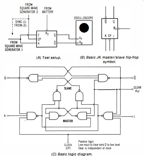
Fig. 4-12. Check of JK flip-flop operation.
(B) Basic 1-of-10 decoder/driver symbol.
(C) Typical package pin-out.
(D) Truth table.
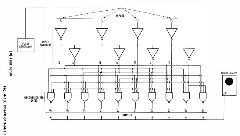
Fig. 4-13 decoder/driver operation.
Procedure: First, with no signal input to any four of the inputs on the decoder/d river, observe the scope response at the various outputs. Next, with signal input at PA only, observe the scope response at the various outputs. Continue with the signal input combinations listed in the truth table, observing the scope response in each step.
Evaluation of Results: In normal operation, the scope will display a pulse or square-wave output only at the decoder/ driver output terminals that correspond to the input signal conditions specified in the truth table. Otherwise, the decoder/d river is defective and should be replaced.
NOTE 4-8 Decoder-Driver Characteristics
The 1-of-10 decoder / driver exemplified in Fig. 4-13 is designed to accept binary-coded-decimal (bcd) inputs and to provide corresponding output states to drive 10-digit incandescent readout displays. All outputs normally remain off for all invalid input conditions. Note that the output gates in the decoder/driver may be provided as open-collector devices; in such a case, the device data sheet will include this information. Also, the test setup will require a load resistor of rated value at each output terminal. Although a 1-0'-10 decoder/driver operates with respect to binary-coded decimal notation, this is of no consequence in test procedures. In other words, the test procedure is concerned only with a determination of whether the device responds In accordance with its associated truth table.
(A) Test setup.
(B) Typical dual Schmitt trigger package pin-out.
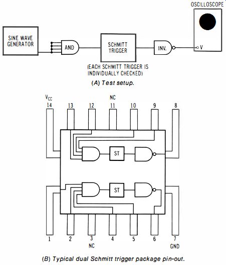
Fig. 4-14. Checking operation of a Schmitt trigger.
4-10. To Check the Operation of a Schmitt Trigger
Equipment: Sine-wave generator, and battery.
Connections Required: As shown in Fig. 4-14, tie all of the AND-gate inputs together and to the output from a sine-wave generator. Connect output from Schmitt trigger to vertical-input channel of scope. Use rated Vee supply voltage.
Procedure: Drive the Schmitt trigger with a suitable peak-to-peak ac voltage, according to the device data-sheet rating.
Observe the scope screen.
Evaluation of Results: In normal operation, a square wave will be displayed on the scope screen; the square wave should have the same repetition rate as the sine-wave frequency.
In other words, a Schmitt trigger normally operates as a waveform squaring circuit. For a comprehensive test, check the AND-gate inputs individually-there is normally zero output from the Schmitt trigger unless all of the AND-gate inputs are simultaneously driven logic-high, or logic-low.
4-11. To Check the Operation of a True/Complement Zero/ One Element
Equipment: Square-wave generator, and battery.
Connections Required: Connect output from square-wave generator to data inputs of true/ complement zero/ one element, as shown in Fig. 4-15. Connect outputs from device to vertical-input channel of scope. Connect control inputs in turn to a logic-high source (battery) or to a logic-low source (ground). Use rated Vcc voltage.
Procedure: With both control inputs logic-high, observe the A1 - Y1 response on the scope screen; continue through A4-Y4
Repeat procedure with both control inputs logic-low, and with one control input logic-high while the other control input is logic-low.
Evaluation of Results: As indicated in the truth table, the square-wave output normally duplicates the square-wave input on each channel when B is logic-high and C is logic-low. However, the square-wave output is normally inverted (complemented) when B and C are both logic-low. If B and C are both logic-high, all outputs are normally logic-low, and there is no square-wave passage. Or, when B is logic-high and C is logic-low, all outputs are normally logic-high, and there is no square-wave passage. Otherwise, the device is defective and should be replaced.
NOTE 4-9 True/Complement Zero/One
Element Function True/complement zero / one elements function to pass a binary number unchanged, or to complement the number in passage. Thus, 1011 can be outputted as 101 1, or it can be outputted as 01 00. This 101 1 output is called the true mode of operation, whereas the 0100 output is called the complementary mode of operation. A true/ complement function is basic in arithmetic and logic units (alu's), because addition occurs when the data is true, and subtraction occurs when the data is complementary.
All arithmetical operations are performed by adders in conjunction with true/complement elements and storage devices such as shift registers.
4-12. To Test the Operation of a Parity Checker/Generator
Equipment: Square-wave generator, and battery.
Connections Required: Refer to Fig. 4-16. Connect output from generator to each of the input terminals on the device in turn ; then connect generator output to pairs of the device input terminals in turn. Connect device outputs to the vertical-input channels of a dual-trace scope. Connect output enable terminal in turn to a logic-high source and to a logic-low source.
Use rated V" c supply voltage.
Procedure: As each device input is driven by the square-wave signal, observe scope screen as the enable terminal is switched from logic-high to logic-low. Repeat as various pairs of device input terminals are driven by the generator.
(See diagram.)
(A) Test setup.
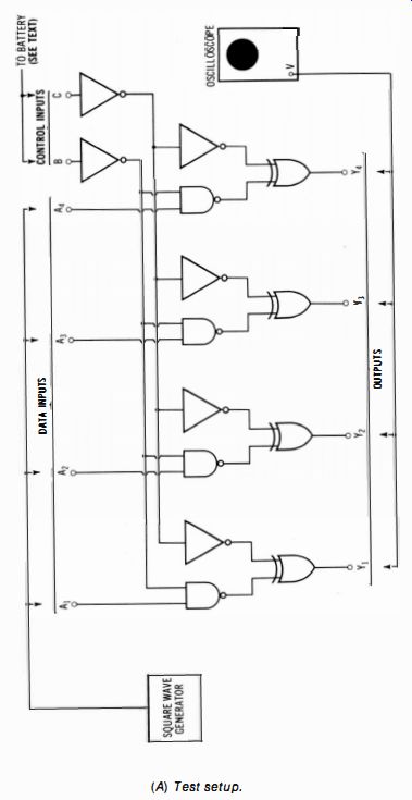
Fig. 4-15. Operating check of a 4-bit true/complement zero/ one element
(B) Basic true/complement zero/one element symbol.
(c) Typical package pin-out.
(D) Truth table.
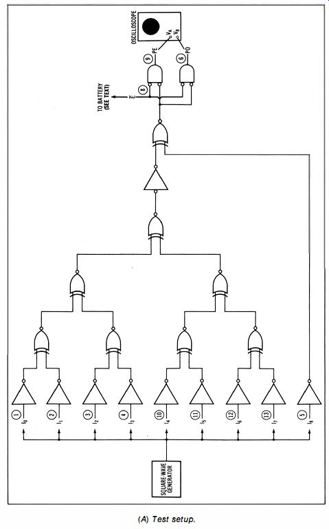
Fig. 4-16. Test of parity checker / generator.
(A) Test setup. (B) Basic parity checker/generator symbol. (c) Typical package pin-out.
Evaluation of Results: In normal operation, an output square wave will be obtained from the PO terminal when one input terminal is driven and the enable terminal is logic-low; no output square wave is normally displayed when the enable terminal is log ic-high. Similarly, an output square wave is normally obtained from the PE terminal when any two input terminals are driven and the enable terminal is logic-low; no output square wave is normally displayed when the enable terminal is logic-high.
NOTE 4-10 Even and Odd Parity
Parity checking is utilized in routine error checks of data processing operations. The exemplified device provides odd and even parity checks for digital words up to nine bits. The even parity output, PE, is normally logic-high if an even number of logic 1 's are applied to the device inputs.
On the other hand. the odd parity output, PO, is normally logic-high if an odd number of logic 1 's is applied to the device inputs. Note that the enable input, E, normally forces both outputs to a logic-low level when a high level is applied to the enable input terminal.