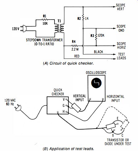
Fig. 5-1 . Test of diode junction action.
| Home | Audio mag. | Stereo Review mag. | High Fidelity mag. | AE/AA mag. |
5-1. To Test a Diode Junction With a Quick Checker
Equipment: Quick checker arrangement as shown in the diagram of Fig. 5-1 . Connections Required: Connect output leads from quick checker to scope, as shown. Connect test leads of quick checker across the diode junction under test.
Procedure: Adjust scope gain controls for suitable size of pattern. Observe shape of displayed pattern (Fig. 5-2). Evaluation of Results: A normal diode will display a rig ht-angled pattern on the scope screen. There may be either one or two right angles, depending on the diode type. The first right angle is the result of forward conduction in the diode. The second right angle (if present) is the result of zener action by the diode.
NOTE 5-1 Operation of Quick Checker
The 10-to-1 stepdown transformer used in the quick checker can be quite small, because the maximum secondary current flow (with red and black test leads short-circuited) is only 11 mA, approximately. The open-circuit output voltage between the leads is approximately 12 V rms; thus, when the leads are shorted, the drop across the 1 K resistor is approximately 30 V p-p. Current flow through the device under test is limited Evaluation of Results: In normal operation, an output square wave will be obtained from the PO terminal when one input terminal is driven and the enable terminal is logic-10W; no output square wave is normally displayed when the enable terminal is logic-high. Similarly, an output square wave is normally obtained from the PE terminal when any two input terminals are driven and the enable terminal is logic-low; no output square wave is normally displayed when the enable terminal is logic-high.
NOTE 4-10 (B) Basic parity checker/generator symbol. (e) Typical package pin-out.
checker / generator.
Even and Odd Parity
Parity checking is utilized in routine error checks of data processing operations. The exemplified device provides odd and even parity checks for digital words up to nine bits. The even parity output, PE, is normally logic-high if an even number of logic 1 's are applied to the device inputs.
On the other hand, the odd parity output, PO, is normally logic-high if an odd number of logic 1 's is applied to the device inputs. Note that the enable input, E, normally forces both outputs to a logic-low level when a high level is applied to the enable input terminal.
(A) Circuit of quick checker.
(B) Application of test leads.

Fig. 5-1 . Test of diode junction action.
... by R1 , by R2, and by the internal resistance of the device. A normal junction has low forward resistance and high back resistance. This difference in junction resistance values produces the characteristic right-angled pattern on the scope screen. If a right angle does not appear in the pattern, the diode is defective and should be replaced. Note that the apparent right angle is actually a section of an exponential curve. However, the diode is swept over a comparatively large voltage interval, with the result that the exponential curve is highly compressed in the pattern, and has the appearance of a right angle.
5-2. To Estimate Resistance Values With a Quick Checker
Equipment: Quick checker.
Connections Required: Connect quick checker to scope, as shown in Fig. 5-1 . Connect test leads from quick checker across resistor under test.
Procedure: Observe the slope of the diagonal line displayed on the scope screen.
Evaluation of Results: Typical pattern slopes produced by resistance values from 100 ohms to 10 kilohms are shown in Fig. 5-3. A "shorted" diode junction never has zero ohms resistance, although its value might be comparatively low.
(A) Black test lead connected to diode cathode.
(c) Waveform of a 3D-volt zener diode.
(B) Black test lead connected to diode anode.
(D) Waveform of a 15-volt zener diode.
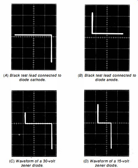
Fig. 5-2. Normal waveforms displayed when the test leads are connected to
a diode.
(E) Waveform of a 7-volt zener diode. (F) Diode polarity identifications.
A short-circuited junction will not produce a right-angled pattern; however, if its internal resistance is appreciable, a 45° angle might be produced, for example. In any case, the slopes will be proportional to the resistance values. For precise calibration of slopes, the test leads from the quick checker can be applied to precision resistors, and the scope controls adjusted for a desired pattern aspect.
5-3. To Check a Bipolar Transistor
Equipment: Quick checker.
Connections Required: With reference to Fig. 5-1 , connect output leads from quick checker to scope. Connect test leads from quick checker to transistor terminals as explained next.
Procedure: (Silicon transistors) . Apply the quick-checker red and black test leads at random to the transistor terminals.
When a waveform is obtained as exemplified in Fig. 5-4, the leads will be connected across the base-emitter junction of the device. Next, connect the red test lead to the collector terminal. Then connect the black test lead alternately to the two remaining terminals of the transistor. A greater vertical deflection will be obtained when the black test lead is connected to the base of the transistor.
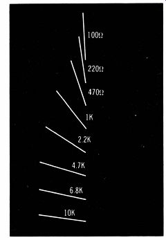
Fig. 5-3. Slopes of screen traces for corresponding values of resistances.
Evaluation of Results: The transistor is workable if the foregoing test results are obtained; the base terminals will also be identified by the test results. In the final step, vertical deflection will be downward at the right and upward at the left for an npn transistor. Deflection is opposite for a pnp type.
NOTE 5-2 Silicon and Germanium Transistor Characteristics
Most transistors are silicon types, and have zener-type conduction through their base-emitter junction; this results in a pattern that has both upward and downward deflection intervals. However, germanium transistors do not have zener conduction, and the foregoing first procedural test cannot be carried out. Hence, the following procedure is used instead: Connect the red and black test leads at random to the transistor terminals. When an open circuit (horizontal line) is displayed on the scope screen, the test leads are connected to the collector and emitter (a small conduction may be observed at the voltage crossover point. Next, connect the black test lead to the base terminal of the transistor. Observe the scope screen; a pnp transistor produces downward deflection at the right, and an npn transistor produces upward deflection at the left of the pattern. (A germanium transistor does not produce both upward and downward deflection intervals.)
5-4. To Check a Bipolar Transistor With a Semiconductor
. Curve Tracer
Equipment: Curve tracer as depicted in Fi g. 5-5.
(A) Pnp base-emitter waveform.
(c) Ppn collector-base waveform with red lead connected to collector.
(E) Black lead connected to base (pnp).
(G) Black lead connected to emitter (pnp).
(B) Npn base-emitter waveform.
(D) Npn collector-base waveform with red lead connected to collector.
(F) Black lead connected to base (npn) .
(H) Black lead connected to emitter (npn).
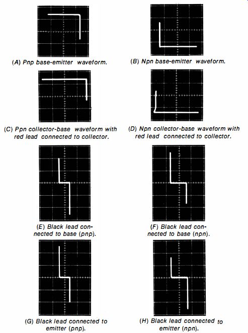
Fig. 5-4. Waveforms normally produced by transistors.
Connections Required: Connect output leads from tracer to the vertical and horizontal input terminals of the scope. Plug transistor under test into the socket provided on the tracer.
Procedure: Set the bias step-voltage control as required for the type of transistor under test. Adjust scope gain controls for suitable size of pattern.
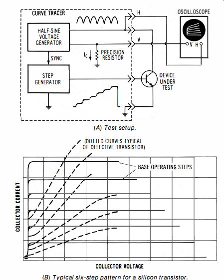
Fig. 5-5. Display of collector family characteristics. (A) Test setup. (B) Typical
six-step pattern for a silicon transistor.
Evaluation of Results: A family of collector characteristics will be displayed on the scope screen if the transistor is in workable condition. A sil icon transistor with very small reverse collector current (very high back resistance) will produce a family of traces that are nearly horizontal. Collector leakage causes the curves to slope uphill on the screen. Low gain causes the family of curves to be compressed at low collector voltage, and to be expanded at high collector voltage.
A germanium transistor normally has lower back resistance than a silicon transistor. In turn, characteristics for germanium transistors tend to slope uphill on the screen to some extent. In case of doubt, compare the test pattern with that produced by a similar known good transistor (or consult the manufacturer's data sheet).
NOTE 5-3 Nonlinear Resistance Indication
Observe that the basic distinction between the quick checker described in Fig. 5-1 and the curve tracer exemplified in Fig. 5-4 is that the latter provides a series of step voltages to obtain a multitrace display. In turn, the slope of a curve in Fig. 5-5 indicates a resistance value, just as the slopes of the traces in Fig. 5-3 represent resistance values.
The slope of a curve indicates the resistance from the collector terminal to the emitter terminal of the transistor under test. Note that the traces are seldom precisely straight, but tend to be curved more or less. This curvature corresponds to nonlinear resistance (resistance wherein the current flow is not directly proportional to the applied voltage). Zero or infinite resistance values (shorted or open transistors) produce approximately vertical or horizontal line patterns, as illustrated in Fig. 5-6. (See also Note 5-4.)
5-5. To Measure the Beta Value (Current Gain) of a Transistor
Equipment: Same as in Fig. 5-4.
Connections Required: Same as in Fig. 5-4.
Procedure: Calibrate the scope with the controls provided on the curve tracer, so that a suitable range such as 10 volts is indicated on the horizontal axis, and a suitable range such as 30 milliamperes is indicated on the vertical axis. Position the pattern as shown in Fig. 5-7.
Evaluation of Results: As illustrated in the diagram, the vertical spacing of successive traces corresponds to a collector current interval termed ?I ('. The base-current steps provided by the curve tracer are set to a base-current interval termed
In turn, the current gain (beta) at a chosen area in the pattern is given by ?I ('/ ?IH' In the illustrated example, ?I(' is measured at a region in the pattern where its value is 9 mA; since the value of ?IH has been set to 0.05 mA, the corresponding value of beta is 180.
NOTE 5-4 Display of NPN and PNP Characteristics
Since npn- and pnp-type transistors conduct in opposite directions, a pnp family of characteristics will be displayed "upside down" with respect to an npn family of characteristics, as depicted in Fig. 5-8. Thus, an npn display is zeroed at the lower left-hand corner of the graticule, ...
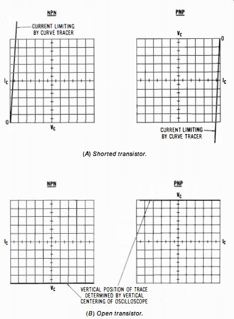
Fig. 5-6. Transistor curves. (A) Shorted transistor. (B) Open transistor.
...whereas a pnp display is zeroed at the upper right-hand corner of the graticule. Note that the scope should have dc-coupled amplifiers; ac-coupled amplifiers will cause trace shift and distort the display. Also, it is desirable that the horizontal amplifier have very high input resistance, because this input resistance shows up in the pattern as apparent transistor leakage resistance. To observe this apparent leakage, switch the transistor in and out, watching for any change (movement) in the base line.
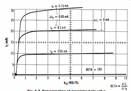
Fig. 5-7. Determination of transistor beta value.
5-6. To Measure the Output Impedance (Resistance) of a Transistor
Equipment: Same as in Fig. 5-4.
Connections Required: Same as in Fig. 5-4.
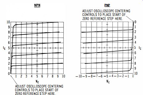
Fig. 5-8. Pnp display is "upside down" with respect to npn display.
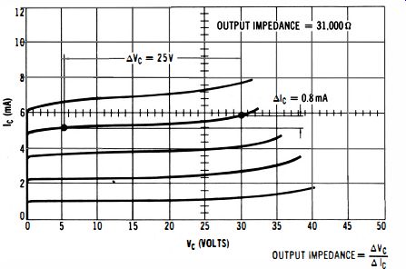
Fig. 5-9. Determination of transistor output impedance.
Procedure: Calibrate the scope for suitable voltage and current ranges such as 50 volts on the horizontal axis and 12 milli-amperes on the vertical axis. Position the pattern as shown in Fig. 5-9.
Evaluation of Results: As indicated in the diagram, the slope of a trace corresponds to a collector-current interval termed ?Ic. This collector-current interval has an associated collector-voltage interval termed ?Vc. In turn, the output impedance denoted by these current and voltage values is given by ?Vc/?lc. In the illustrated example, this ratio is equal to 25/0.0008, or 31,000 ohms. As a general rule, power-type transistors have lower output impedance than small-signal transistors.
NOTE 5-5 Looping and Thermal Runaway
Test procedures should always be conservative, so that the device under test is not overdriven. Conduction of current through a transistor generates heat. If the collector voltage and/or base current results in excessive heating, the traces that are normally displayed change into loops. The size of the loop increases as the amount of overdrive is increased. This condition is incipient "thermal runaway" which will destroy a transistor unless the drive is decreased. Overdrive causes looping to appear in the pattern because the transistor heats up rapidly as the peak of the, drive voltage or current is approached, and then cools to some extent as the peak is passed. Inasmuch as heating occurs before cooling, there is a time lag involved that shows up in the pattern as a looping.
5-7. To Check the Condition of a Transistor In-Circuit
Equipment: Transistor curve tracer.
Connections Required: Remove power from equipment under test ; then connect the curve-t racer test leads to the transistor on the printed-circuit board.
Procedure: Since circuit impedances may shunt considerable base-drive voltage around the transistor, it may be necessary to apply more base-d rive step voltage than in out-of-circuit tests. Occasionally, all of the available drive signal may be shunted away by a very low in-circuit base-emitter resistance, and no curve display can be obtained on the scope screen.
Evaluation of Results: In-circuit patterns generally appear highly distorted, as compared with out-of-circuit collector characteristic patterns (see Fig. 5-10). This distortion is due to in circuit impedance. However, it is possible to interpret various displays. For example, five loops and a base line appear in the npn pattern. This is interpreted to mean that every base voltage step produces additional collector current, and that the transistor is probably workable. The pnp pattern is typical of an oscillator circuit; it seems to indicate serious transistor leakage, although the transistor is normal. In summary, in-circuit pattern evaluation is best accomplished on the basis of comparative tests, or on the basis of experience with specific circuitry.
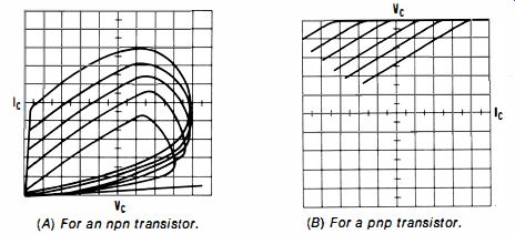
Fig. 5-10. Typical in-circuit curve-tracer patterns. (A) For an npn transistor.
(B) For a pnp transistor.
NOTE 5-6 Impedance Loops Versus Thermal Loops
The loops shown in Fig. 5-1 0 are typical impedance loops, caused by RC or RL circuitry. It is easily possible to distinguish between such impedance loops and the thermal loops described in Note 5-5. Thus, the loop size decreases and disappears as the drive is decreased, in the case of a thermal loop. On the other hand, an impedance loop does not disappear as the drive is decreased.
5-8. To Select a Pair of Matched Transistors
Equipment: Transistor curve tracer.
Connections Required: Insert the various transistors from an assortment successively into the test sockets on the curve tracer.
Procedure: Observe the screen patterns produced by the chosen transistors.
Evaluation of Results: A pair of matched transistors will produce patterns that are virtually identical. In complementary symmetry amplifiers, a pnp transistor is to be matched by an npn transistor. Therefore, the test patterns will have opposite polarity, as depicted in Fig. 5-11. However, the pnp pattern matches the npn pattern if it is a mirror image.
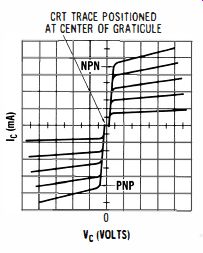
Fig. 5-11. Mirror-image patterns indicating that the npn transistor matches
the pnp transistor.
NOTE 5-7
"Vertical Roll" In Loop Pattern
If excessive heat is generated in a transistor while testing with a curve tracer, the condition becomes apparent in the scope pattern (Fig. 5-12) . Looping appears in the traces, because the collector current does not increase and decrease at the same rate as the sweep voltage increases and decreases. As the sweep voltage starts from zero, the transistor is comparatively cool. The transistor temperature increases to a maximum at the peak of the sweep voltage, and increasing temperature causes additional collector-current flow and additional heat. Then, as the sweep voltage decreases, a time lag is involved in cooling of the transistor.
The top portion of a loop shows the increasing sweep current, and the bottom portion of the loop shows the decreasing sweep current. Note also that with some transistors, the collector current will droop at the high end of the curve-an increase in temperature is causing a decrease in collector current. If thermal runaway starts, "vertical roll" appears; the entire family of curves moves in the direction of higher collector current, and can soon result in transistor burn-out.
5-9. To Check Nonlinearity in Transistor Current Gain
Equipment: Transistor curve tracer.
Connections Required: Same as in 5-4.
Procedure: Observe the screen pattern produced by the transistor under test.
Evaluation of Results: With reference to Fig. 5-13, plot an imaginary line along the ends of the curves; this is the "test load line." Next, plot an "operating load line" in parallel with the test load line, but intersecting the zero I_c line at the desired operating delta I_c: for the transistor. Then, measure and compare the changes in collector current (did between the curves on operating load line. If these changes are the same, the transistor is linear in the test region. On the other hand, if these changes are not the same, the transistor is nonlinear in the test region. In Fig. 5-14, there is some nonlinearity displayed.
In other words, because delta 9mA is unequal to d1 1 mA, amplitude distortion will occur in the test region. For example, an input signal of ±0.05 mA will produce an output signal of +9 mA and -11 mA.
NOTE 5-8 Variation in Nonlinearity
Transistor gain is not entirely constant, and may be quite nonlinear.
The amount of nonlinearity is dependent upon the region of measurement in the pattern. Non-linearity may be desirable or undesirable, depending upon the application of the transistor. Nonlinearity should be measured along a load line, as has been explained; this method more nearly duplicates circuit operating conditions than if the nonlinearity is measured at a specific value of Vc>:. A load resistance causes circuit operation along a load line, because a change in collector current produces a change in voltage drop across the load, and in turn produces a change in collector voltage.
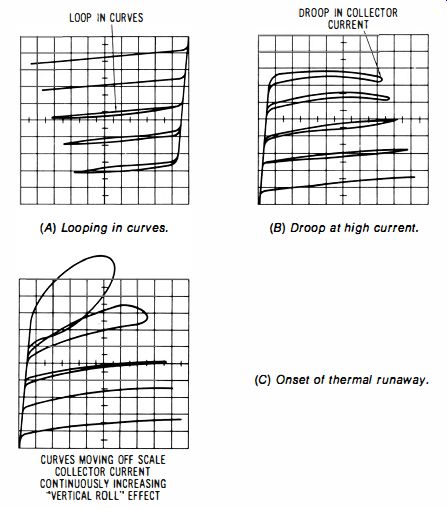
Fig. 5-12. Evidence of transistor heating in scope patterns.
(A) Looping in curves. (B) Droop at high current. (C) Onset of thermal runaway.
5-10. Transistor Breakdown Voltage Measurement
Equipment: Transistor curve tracer.
Connections Required: Same as in 5-4.
Procedure: Display the collector family on the scope screen, with reduced horizontal width. Then, increase the sweep voltage control on the curve tracer until an upturn in collector current is observed at the tai l of the curves. (See Fig. 5-1 5.) Evaluation of Results: The upturn in collector current at the on set of breakdown is very sharp for most transistors, although it is somewhat gradual for a few types. Read the collector ...
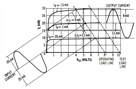
Fig. 5-13. Measurement of nonlinearity In transistor characteristics.
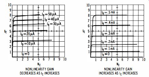
Fig. 5-14. Two types of nonlinear collector family characteristics.
... voltage value at which the curve upturn starts along the calibrated horizontal axis.
NOTE 5-9 Breakdown Testing Technique
The measured breakdown voltage will normally be greater than the breakdown voltage rating in the transistor data sheet. Otherwise, the transistor is defective and should be replaced. If the breakdown voltage rating is not available, a practical rule of thumb is that the breakdown voltage should be double the value of the collector supply voltage of the circuit ...
(A) Abrupt breakdown. (B) Gradual breakdown.
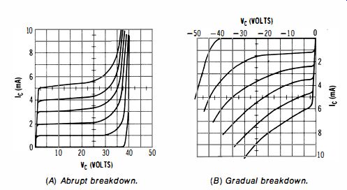
Fig. 5-15. Patterns observed during breakdown voltage measurements.
... in which the transistor is to be used. Breakdown voltage measurements should be made carefully, so that current upturn is not substantial, with the associated danger of thermal runaway and transistor burnout. For the same reason, breakdown voltage tests should not be prolonged.
5-11. Transistor Saturation Voltage and Resistance Measurement
Equipment: Transistor curve tracer.
Connections Required: Same as in 5-4.
Procedure: Display the collector family and note that the knee of each curve (Fig. 5-1 6) occurs at approximately the same collector voltage, regardless of base current.
Evaluation of Results: The value of the saturation voltage VeE(sat) is defined as the collector voltage at the knee of a curve. The saturation resistance reE(sat) is equal to Velie; it is equal to the collector voltage divided by the collector current for a given value of base current in the collector saturation region.
NOTE 5-10 Saturation Voltage and Resistance Ratings
For measurement of saturation voltage in comparison to data-sheet specifications, the base current and collector current should be noted at the point of measurement. The manufacturer's rating is the maximum value at which the knee should occur. In other words, if the rating is on or above the knee, the transistor is acceptable. Note that to measure saturation voltage on the curve tracer, only the saturation region of the characteristics need be displayed; this is the low collector-voltage region up to and including the knee of each curve. Thus, the display can be expanded, using a low-voltage horizontal calibration value, such as 0.2 volt per division. This facilitates accurate measurement of low collector voltage values. Data sheets usually specify saturation-resistance values as maximum acceptable limits.
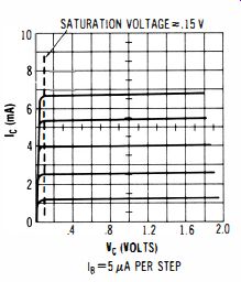
Fig. 5-16. Measurement of saturation voltage.
5-12. To Display a Drain Family of FET Characteristic Curves
Equipment: Transistor curve tracer.
Connections Required: Same as in 5-4.
Procedure: Keep one hand grounded while handling the FET with the other hand, to avoid device damage from static electricity. Set tracer controls for FET test. Ground the shield of the FET (if present). In the case of a dual-gate device, ground the gate which is not being driven in the test. Be careful not to overdrive and damage the FET. Evaluation of Results: Compare the drain family displayed in the screen pattern with the curves specified in the device data sheet. A normal device will have rated tolerances. If the FET is out of tolerance, it is defective and should be replaced (Fig. 5-17).
NOTE 5-11
Depletion and Enhancement Types of FETs
FET characteristic curves show the relation of drain current versus drain voltage at various gate voltages. FET breakdown voltage may be checked and measured in the same manner as for bipolar transistors.
When checking FETs, a curve tracer is set to apply constant-voltage steps to the gate, instead of constant-current steps as in the case of (A) N-channel FET. (B) P-channel FET.
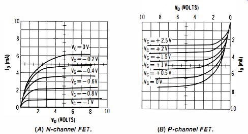
Fig. 5-17. Typical FET drain family characteristics.
... base drive to a bipolar transistor. Most FETs are of the depletion type, and the zero-volt step corresponds to the highest drain current in the pattern. A few FETs are designed as enhancement devices, which normally have zero drain current at zero gate voltage. To check an enhancement FET, a suitable forward bias voltage must be connected in series with the gate-source lead. In turn, the enhancement device can be tested in the same manner as a depletion device.
5-13. To Check the Drain Family Characteristics for a Dual
Gate FET
Equipment: Transistor curve tracer.
Connections Required: Same as in 5-4, except that the unused gate is connected to the source. In the second part of the test, the unused gate is returned to the source through an adjustable bi as voltage.
Procedure: Same as in 5-12, except that a separate test is made for each gate. Follow up with a comparison test in which the drain family characteristics are displayed with the undriven gate returned to the source through low, medium, and high values of bias voltage.
Evaluation of Results: Consult the data sheet for the device, and observe whether the FET is within rated tolerances in each part of the test procedure. Note that dual-gate FETs are used, . for example, in agc circuitry and in heterodyne mixer circuitry; both gates have control of the drain current flow.
5-14. To Measure the Transconductance of an FET
Equipment: Transistor curve tracer.
Connections Required: Same as in 5-4.
Procedure: Observe the change in drain current (10) that results from a corresponding change in gate voltage (VG) within the region of the characteristics chosen for measurement (Fig. 5-18). Evaluation of Results: Transconductance is measured in mhos, and is equal to a given change in drain current divided by the associated change in gate voltage:
aiD g m = aVG
For example, in Fig. 5-1 8 a change of 1.1 mA in drain current is caused by a change of 0.5 volt in gate voltage. Accordingly, the transconductance of the FET in the region of measurement is 2200 micromhos (,umhos) .
NOTE 5-12 Voltage- and Current-Operated Devices
(PINCHOFF DENOTES ZERO DRAIN CURRENT: THE PINCHOFF VOLTAGE IS THE GATE VOLTAGE REQUIRED TO BRING THE DRAIN CURRENT TO ZERO
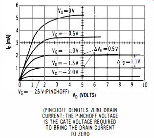
Fig. 5-18. Example of transconductance measurement.
The gain of an FET is measured in terms of transconductance because the gate draws negligible current; an FET is said to be a voltage-operated device. On the other hand, the gain of a bipolar transistor is measured in terms of a current ratio (beta) because the base draws current; a bipolar transistor is said to be a current-operated device. In turn, the gain of an FET in micromhos cannot be directly compared with the gain of a bipolar transistor in beta units. However, it may be noted that the gain of a bipolar transistor can be measured in terms of transconductance, if desired. This is done by measuring the change in collector current that results from an associated change in base voltage. In the majority of practical applications, it is preferable to consider the gain of a bipolar transistor in beta units.
5-15. To Determine the Pinchoff Voltage of an FET
Equipment: Transistor curve tracer.
Connections Required: Same as in 5-4.
Procedure: Start display of the pattern with a small step voltage which provides all of the available curves (such as six curves). Then, increase the step-voltage setting until the last curve disappears (merges with the next-to-the-last curve along the zero current axis). In Fig. 5-19, this increase in step voltage causes two of the latter curves to disappear.
(A) Pinchoff is not reached with D.S-volt steps in gate voltage.
(B) Pinchoff is reached with 1-volt steps in gate voltage.
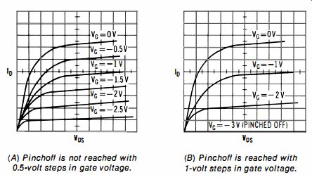
Fig. 5-19. Determination of pinchoff voltage.
Evaluation of Results: The pinchoff voltage is the gate voltage that corresponds to the zero-current level in the pattern. For example, in Fig. 5-1 9, pinchoff occurs in the range between -2.5 and -3 volts. If a more precise measurement is desired, connect an external bias source to the gate of the FET, and adjust the bias voltage exactly to pinchoff, as indicated on the scope screen.
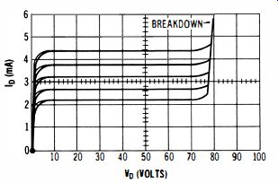
Fig. 5-20. Example of FET breakdown voltage measurement.
5-16. To Measure the Breakdown Voltage of an FET
Equipment: Transistor curve tracer.
Connections Required: Same as in 5-4.
Procedure: Display the drain family of characteristics. Increase the curve-tracer sweep voltage until the curves show the onset of breakdown (see Fig. 5-20). Evaluation of Results: The breakdown voltage is reached at the point where the curves begin to show an abrupt up-shoot in drain current. Keep the test time short, to avoid possible damage to the FET.
5-17. To Check a Silicon Controlled Rectifier for Forward Blocking Voltage
Equipment: Transistor curve tracer.
Connections Required: As depicted in Fig. 5-21 , connect the SCR anode terminal to the collector jack of the curve tracer; connect the SCR gate terminal to the base jack; connect the SCR cathode terminal to the emitter jack.
Procedure: Set the step-selector control to zero volt (this is the ICES position for a typical tracer) ; set the polarity control to npn. Then increase the sweep-voltage setting until the SCR "fi res"; in other words, the anode current abruptly increases and the anode voltage drops to nearly zero.
Evaluation of Results: Read the highest anode voltage value in the display on the calibrated screen.
SCR CONNECTIONS TO CURVE TRACER.
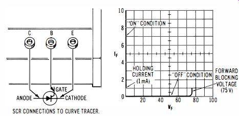
Fig. 5-21. Measurement of forward blocking voltage for an SCR; holding current
is also displayed.
This highest value is defined as the maximum forward blocking voltage. Any anode current at anode voltage below the firing point is forward leakage current and it can be read directly from the display.
NOTE 5-13 SCR Function
An SCR or thyristor is a four-layer pnpn device with three terminals: cathode, anode, and gate. It operates similarly to a diode in its "on" state. However, an SCR also has an "off" state in which it will not conduct in either direction. If its forward blocking voltage is exceeded, the SCR normally "turns on." It will then stay on until the anode-cathode current drops below a certain value called the holding current. The forward blocking voltage is the maximum anode-cathode voltage in the forward direction that the SCR can withstand before conduction, with the condition of zero gate current.
5-18. To Measure the Reverse Blocking Voltage for an SCR
Equipment: Transistor curve tracer.
Connections Required: Same as in Fig. 5-21 . Procedure: Same as in 5-1 7 except that the polarity control is set to its pnp position.
Evaluation of Results: Read the highest voltage value on the screen at which voltage breakdown occurs with an abrupt in
crease in anode current. Any anode current that flows at voltages below the breakdown point is reverse leakage current and can be read directly from the display.
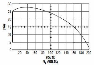
Fig. 5-22. Example of forward conduction at 200 volts, followed by holding-current
indication of 5 mAo
5-19. To Measure the Holding Current for an SCR
Equipment: Transistor curve tracer.
Connections Required: Same as in Fig. 5-21 . Procedure: Same as in 5-1 7.
Evaluation of Results: Observe the lowest current value displayed for the "on" condition of the SCA. This is defined as the holding current. Note that the holding current can also be measured with the step-selector control set to one of its "current per step" positions, so that less sweep voltage is required to drive the SCR into its "on" condition (Fig. 5-22).
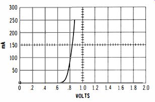
Fig. 5-23. Example of forward voltage drop display for an SCR.
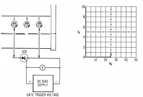
Fig. 5-24. Check of gate trigger voltage for an SCR.
5-20. To Measure the Forward Voltage Drop of an SCR
Equipment: Transistor curve tracer.
Connections Required:
Same as in Fig. 5-21. Procedure: Increase the horizontal sensitivity of the oscilloscope and display a low voltage portion of the forward voltage (Fig. 5-23). Then increase the current-per-step control setting so that the sweep voltage may be reduced. The vertical sensitivity of the scope may be reduced to 10 mA per division for a greater voltage/ current range.
Evaluation of Results: Read the forward voltage value directly from the display.
5-21. To Measure the Gate Trigger Voltage for an SCR
Equipment: Transistor curve tracer, dc bias supply with meter.
Connections Required: Connect equipment as shown in Fig. 5-24.
Procedure: Same as in 5-17, but set the sweep voltage to a specified forward anode-cathode voltage, and increase the dc bias value until the SCR switches on. Observe the value of gate voltage at which switching occurs. Alternatively, set
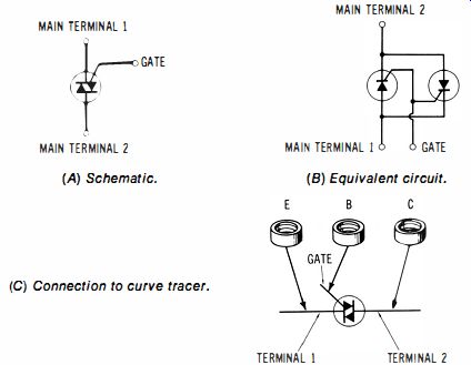
Fig. 5-25. A triac consists of two paralleled and oppositely polarized SCRs.
(A) Schematic. (B) Equivalent circuit. (C) Connection to curve tracer.
... the dc bias supply to a specified gate voltage, and increase the sweep voltage until the SCR switches on. Observe the peak value of sweep voltage that is required for switching action.
Evaluation of Results: The turn-on point of an SCR depends on both the forward voltage and the value of gate voltage that are applied. As the gate voltage is increased, less forward voltage is required to switch the SCR, and vice versa. Thus, the SCR is evaluated for the bias voltage with respect to the sweep voltage required for switching action.
NOTE 5-14 Triac Operation
Triacs are four-layer pnpn devices that have the same characteristics in both directions; they are used in ac applications. As depicted in Fig. 5-25 a triac is the equivalent of two SCRs connected in parallel, but oriented in opposite directions. A triac has a main terminal 1, a main terminal 2, and a gate terminal. Triacs are tested in the same manner as SCRs except that forward tests are repeated to determine the characteristics in both directions. Note that there is no reverse blocking voltage measurement.