BY REG WILLIAMSON and ALAN WATLING, Contributing Editor
Cont. from: A NEW CONTROL PREAMP: BACK TO THE FUTURE PART 1
NOW WE COME to a complete pre-amplifier circuit (Photo 2) and you'll see right away, I favor the tilt control and the steep cut filter. Alan Watling has done a splendid job of de signing a suitable circuit card, as well as constructing a prototype we have both given a good workout. The concept of a feedback-type gain control came somewhat late for its inclusion in ...
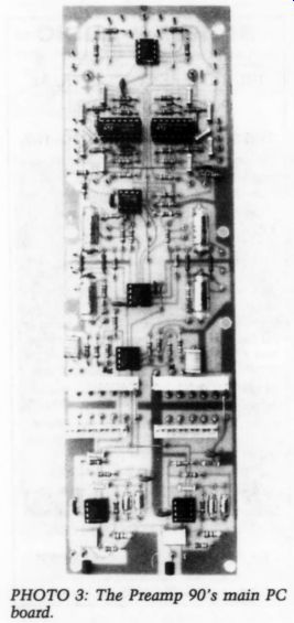
The Preamp 90's main PCB.
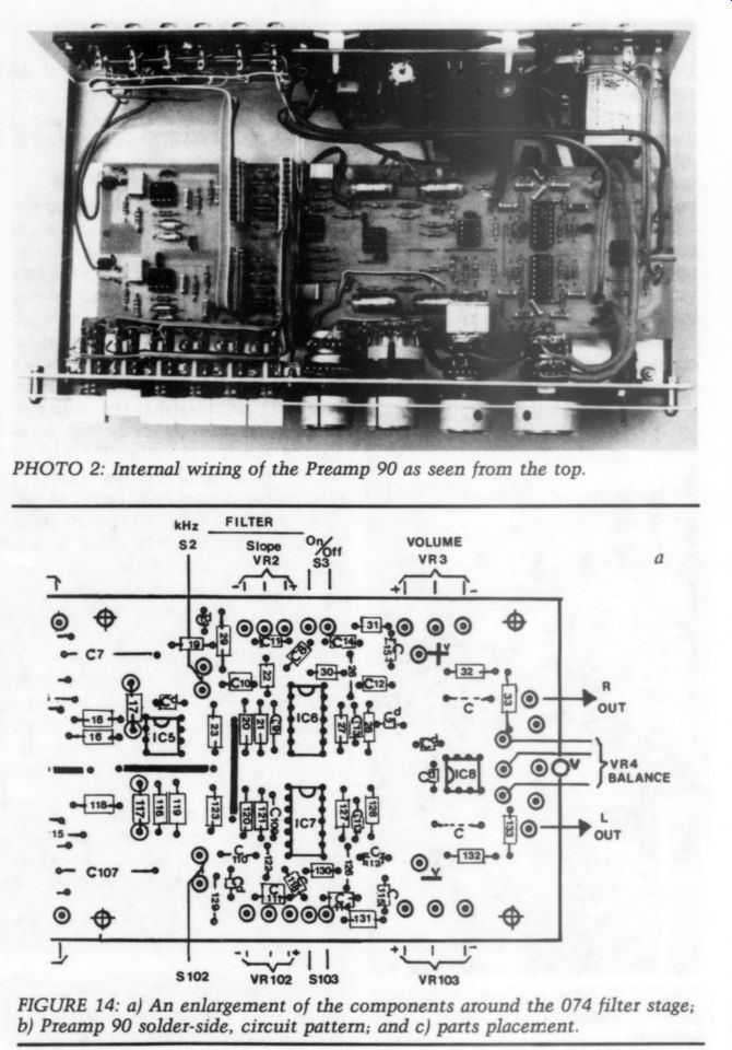
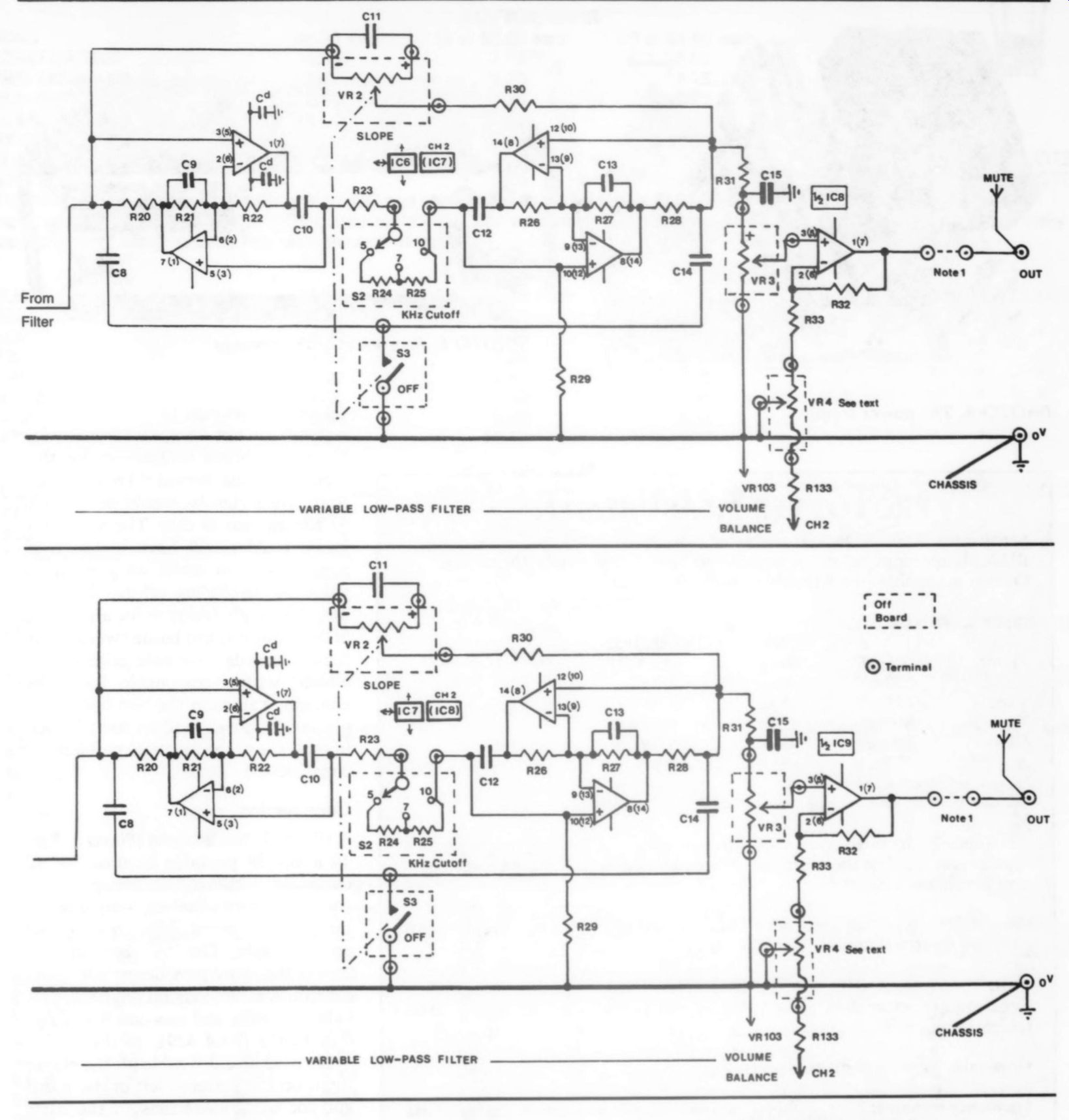
Photo 2; FIGURE 14: a) An enlargement of the components around the 074 filter stage; b) Preamp 90 solder-side, circuit pattern; and c) parts placement.
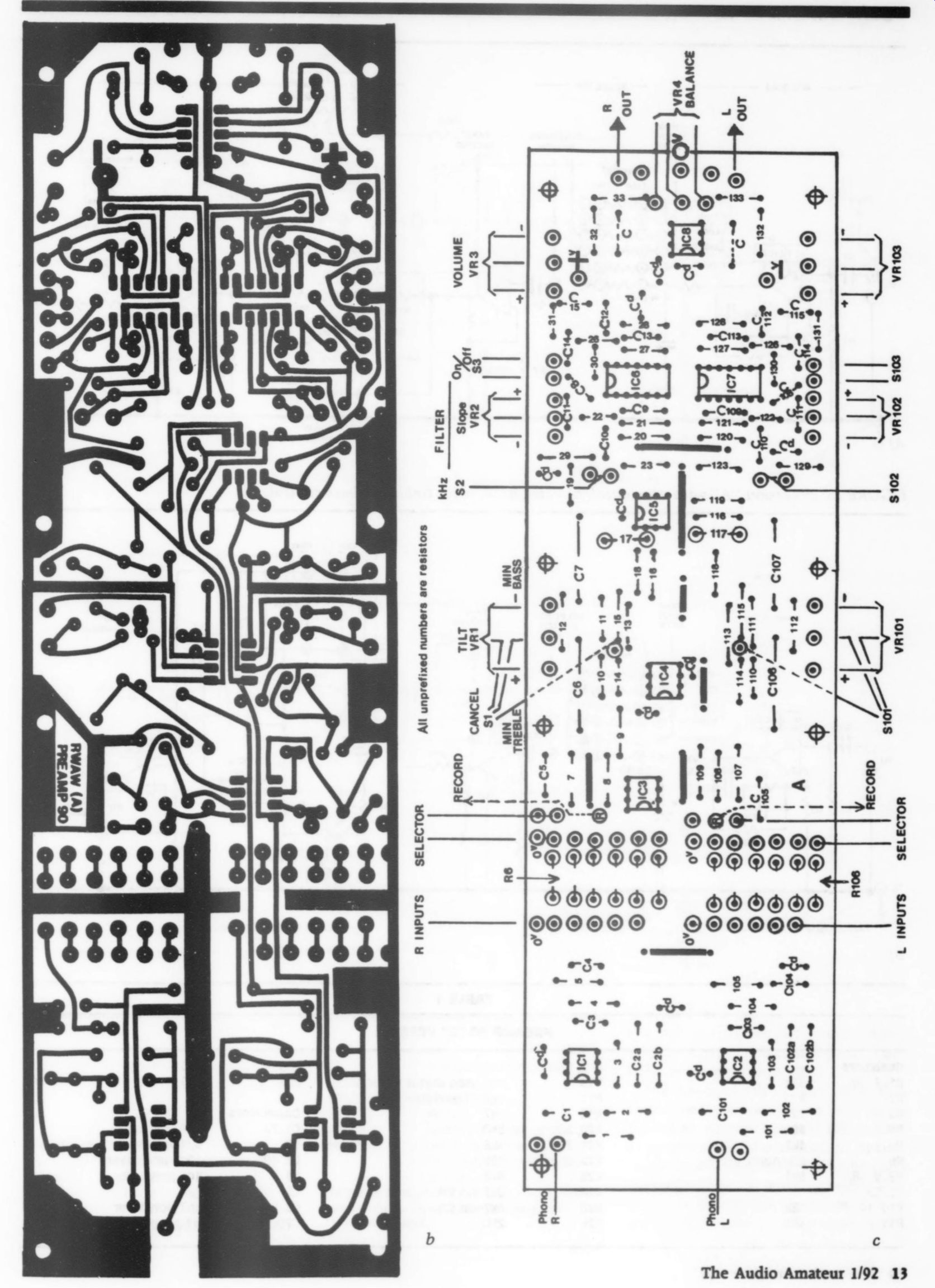
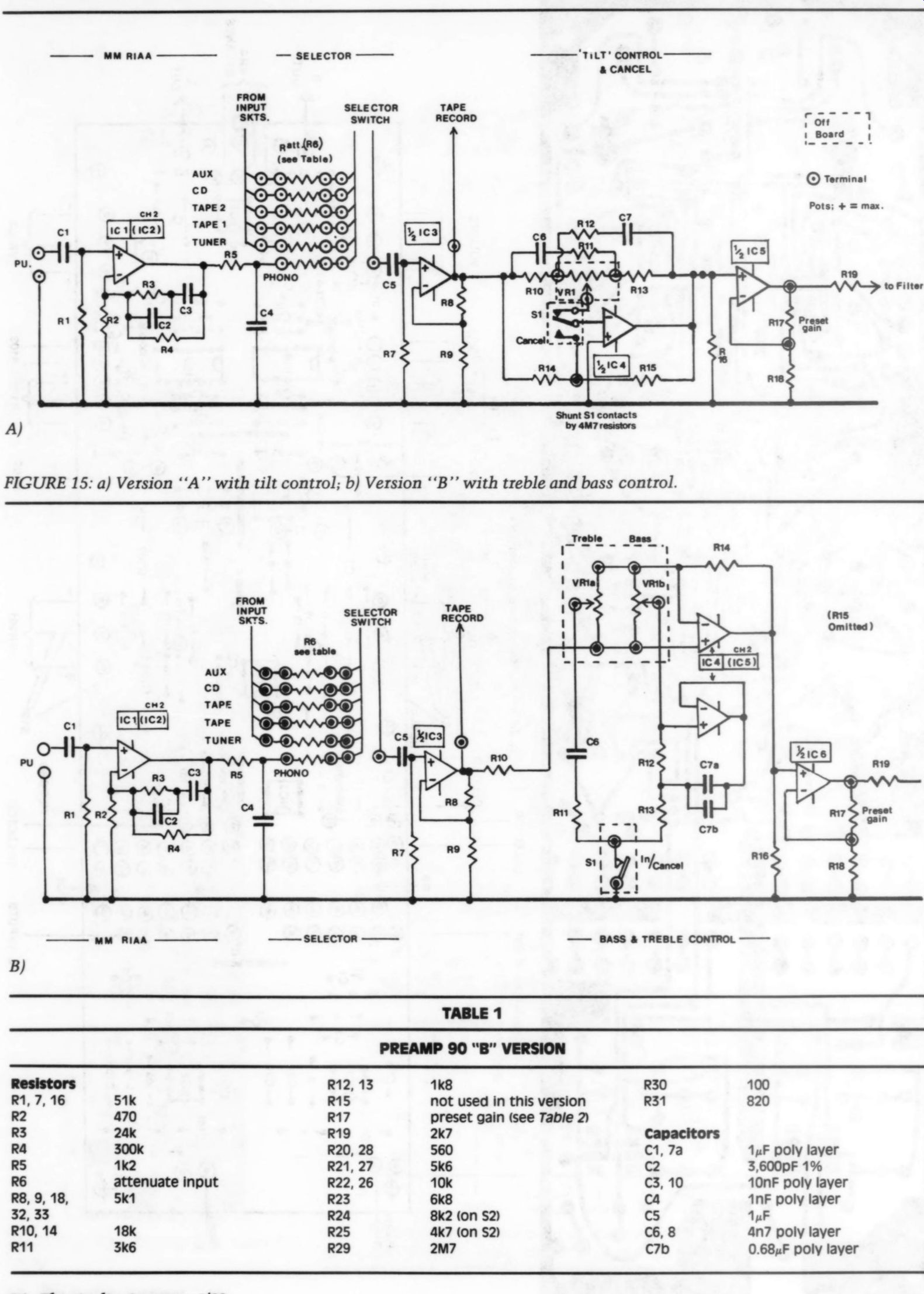
FIGURE 15: a) Version “A” with tilt control; b) Version “B” with treble and bass control.
TABLE 1 PREAMP 90 “B” VERSION
... the full design; so the output stage, with facilities for balancing the channels, is sensibly orthodox.
My principal role as designer in this collective project with Alan Watling included an attempt to make life as easy as possible for the constructor, in that inexpensive components may be used in nearly all cases. It is regrettable that many of my fellow designers fail to realize that expensive E96 or even E48
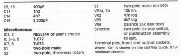
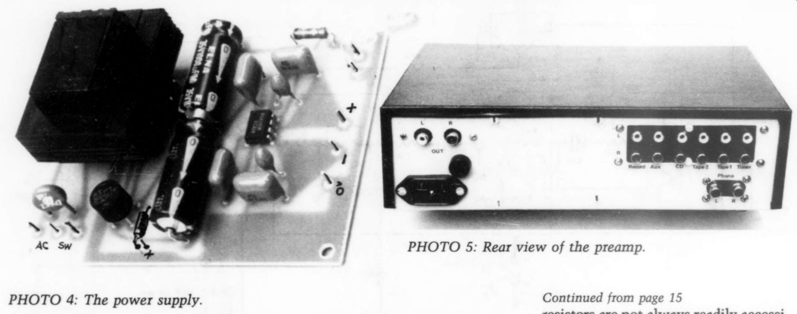
PHOTO 4: The power supply.
PHOTO 5: Rear view of the preamp.
----------------
PROTOTYPE MEASUREMENTS
Sensitivity: Basic 150mV available at Z = 51k-Ohm.
RIAA phono input 2.5mV to match this sensitivity at selector switch.
Output selectable (see R16 table) from 300mV to 1V.
Input sensitivity: * R6
OVERLOAD
Phono 2.5mV strap 64mV Tuner 150mV strap 1.8V Tape 1 775mV 180k 8.0V Tape 2 300mV 51k 3.6V CD 300mV 51k 3.6V Aux.
300mV 51k 3.6V
*Record out 310mV all cases.
**Typically set for video recorder audio output.
The input Z obviously varies for different values of R6, but this is usually unimportant, unless the source needs special matching. R106 is complementary for channel 2.
Output: R16 (R116) 2k7 for 350mV out; 8k2 for 600mV out (relates to input overload figures above); 15k for 1V out.
SNR: Phono input, S/C, -65dB (for IC NE5534A).
Other inputs better than - 70dB. Worst case is filter “in” at 10kHz, maximum slope.
Crosstalk: 1kHz -45dB (see text).
Frequency response: 20Hz-50kHz, +0, - 0.5dB; RIAA variation, 20Hz-20kHz within 0.4dB; tilt and filter response (see graphs).
System phase: inverting.
Balance control characteristic: + 4dB on preferred output; - 1dB on other output.
Output offset: L: -3mV, R: - 1mV Distortion: see text.
------------------------
...resistors are not always readily accessible to the home builder-or for that matter are capacitors of 0.1% tolerance.
Alan, quite rightly, would be the first to remind me of this. The worst the home builder will have to do is, in some cases, to make up a specified value by paralleling off-the-shelf values. Although designed for a nominal 500mV output, the home tweaker can have a field day, because gains can be altered within reasonable limits by changing values in the two buffer amplifiers. So now, I will let Alan fill you in on some of the practical problems of construction.
Construction
A 10” by 3” board layout (Photo 3, Figs. 14 a and b) provides location for all components (Photo 2) except input sockets, potentiometers, source selector (for six inputs), filter switch, and power supply. The “A” version (Fig. 15a) of the board provides a “tilt” tone control, the “B” version (Fig. 15b) provides the treble and bass controls of Fig. 1 in Part 1 (TAA 4/91, p. 10).
We used shielded cable for the phono input on the extreme left of the board and for the connections to the filter switch and slope functions. The rest were solid core wire in single or rib bon formation, which proved to be more than adequate in performance measurements.
(Of interest to the perfectionist, I built a no-compromise version of the tone control and filter stages for my own modular control unit, using a double-sided board with ground-plane earthing and integral pots and switches. It cost me twice as much in materials and four times as long to build. The result was less than a decibel better on signal to-noise ratio and identical on program performance.) First, fit the terminal pins for the off board connections so they can be tapped in from the foil side of the board before it gets cluttered with components. There are more than a hundred of these, although you can save some by terminating the input and selector switch wiring directly to the foil pads.
In the prototype I used board-mounted plugs and sockets to facilitate testing.
Difficult Circuit
There are seven straps (jumpers) on the A board (and five on the B board) to wire in first. Most of these are to route the + and - power supplies to the ICs, so insulated wire is preferable.
Next, fit the IC sockets, using notch identification for correct orientation.
-------------- TABLE 2
Resistors R1 1k8 Capacitors Cc1,2 1,000 uF/35V C3-6 0.1 uF Cc7,8 10 uF/25V tantalum
Miscellaneous Bridge 2A
D1 transient limiter
D2 1N4002 LED terminal pins RF filter line socket entry type SW. 250v, 2A m 15-0-15V sec. 200mA min.
4195 +15V tracking regulator no socket: directly soldered to foil
---------------------
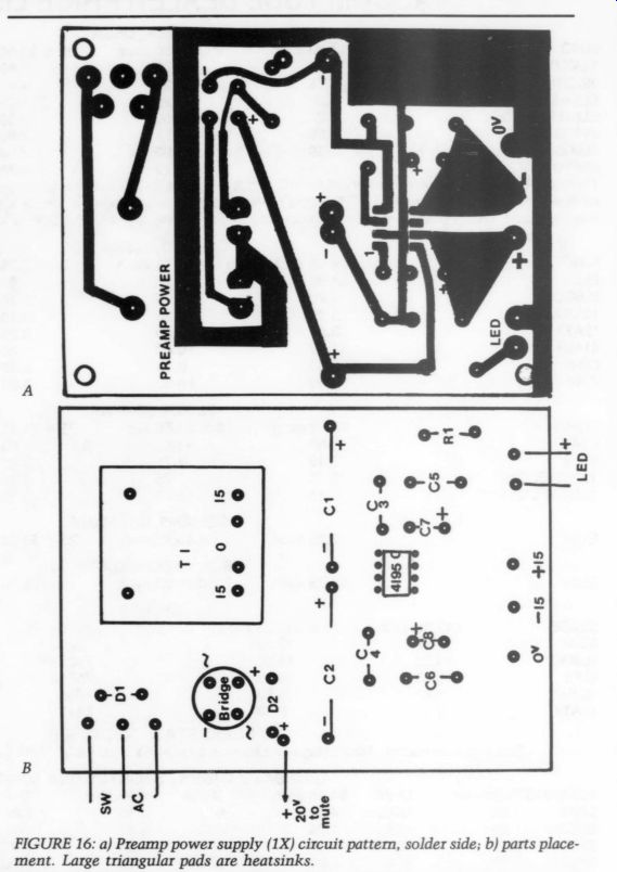
FIGURE 16: a) Preamp power supply (1X) circuit pattern, solder side; b) parts placement. Large triangular pads are heatsinks.
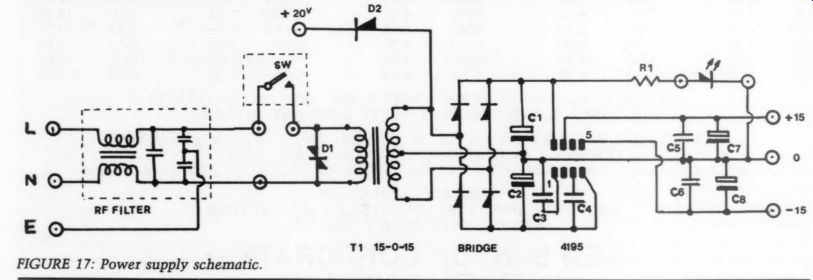
FIGURE 17: Power supply schematic.
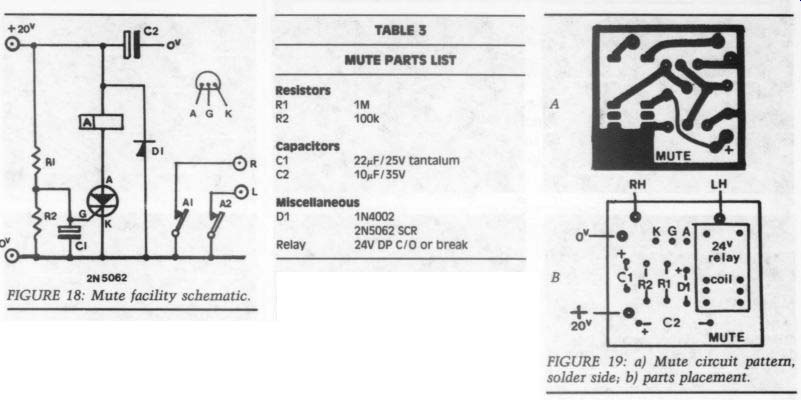
FIGURE 18: Mute facility schematic.
FIGURE 19: a) Mute circuit pattern, solder side; b) parts placement.
---------
TABLE 3 MUTE PARTS LIST Resistors R1 R2 Mm 100k
Capacitors C1 C2 22,F/25V tantalum 10 uF/35V
Miscellaneous D1 1N4002 2N5062 SCR Relay 24V DP C/0 or break
-------------
The foil pattern deliberately avoids tracks between IC tags, since experience shows these are a common source of solder bridges in amateur work. At this point it pays to solder up-to-date carefully and do a continuity check from the power + and - supplies to the relevant pins of the ICs. Note the different tag numbers on the 072 and 074. Resistors next, then capacitors. No electrolytics, so no polarity problems.
The only difficult capacitors are 5,600pF ones in the tilt circuit. Keep the heat away from these rather bulky caps. Two of the resistors in each channel are on the filter frequency switch.
Components around the 074 filter stage are rather close and need extra care. An enlarged diagram of this part of the board is shown in Fig. 14a. Double-check the construction here, as this is a difficult part of the circuit to analyze for faults.
The Prototype
Input connections to the first row of pins on the board are tuner, tape 1, tape 2, CD, and auxiliary. The phono input ...
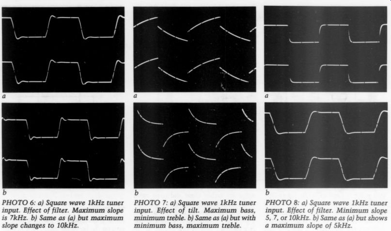
PHOTO 6: a) Square wave 1kHz tuner input. Effect of filter. Maximum slope is 7kHz. b) Same as (a) but maximum slope changes to 10kHz.
PHOTO 7: a) Square wave 1kHz tuner input. Effect of tilt. Maximum bass, minimum treble. b) Same as (a) but with minimum bass, maximum treble.
PHOTO 8: a) Square wave 1kHz tuner input. Effect of filter. Minimum slope 5, 7, or 10kHz. b) Same as (a) but shows a maximum slope of 5kHz.
... is on the extreme end of the board- use ferrite beads on the wires to these terminals to prevent RF pickup. Two turns of the connecting wire (not the shield) suffice.
All input ground or shield connections should be made to the nearest OV tag on that side of the board-do not use your chassis or metal box for this purpose. The chassis or screening box should be connected to the 0-V terminal on the power supply or the output sockets.
The selector switch has six choices to pass on to the first buffer stage. A six way pushbutton assembly was used in the prototype so that the undesired in puts could be easily grounded. A rotary switch is a less expensive option if grounding is not required.
Power Supply
Acceptance tests were made with a 3A regulated and stabilized bench supply.
No detectable difference in measurement or program resulted from the final use of a + 15V tracking regulator design ed for 50mA per rail. The actual demand is 40mA, and the chip temperature does not exceed 41°C. A separate raw 20V supply is on the power board to operate the fast-mute board which in my case is soldered across the output terminals (Figs. 16a and b). Since this includes a relay it should not be connected to the + or -15V supply.
NOTE: For References and biographies of the two authors, see the last page of Part 1 of this article, TAA 4/91, p. 19.
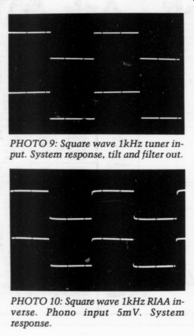
PHOTO 9: Square wave 1kHz tuner in put. System response, tilt and filter out.
PHOTO 10: Square wave 1kHz RIAA in verse. Phono input 5mV. System response.
The output stage of the preamp is directly coupled (Fig. 17). If the resulting offset voltages of a few millivolts are an embarrassment, fit a capacitor to match your needs in the dotted position shown; otherwise solder straps in that position.
During the development tests, equal importance was given to critical measurements and careful listening. The subjective effects of varying levels of crosstalk were critically compared, even to the extent of using an adapter fitted with two 071s to replace the circuit 072. The decoupling capacitors were positioned for optimum results on oscilloscope traces. Finally, the proto type was listened to in both our homes on top-grade material.
VR;, the balance control, should ideally be a 25k wire-wound component. The inevitable wiper-to-track resistance of a carbon or ceramic component increases crosstalk to -45dB, which is not theoretically acceptable, although practical tests showed that it was undetectable on program.
The mute facility (Fig. 18), shown as a separate small board for soldering direct to the output phono sockets (Figs. 19a and b), is needed because the gain control comes before the output 072. The switch-on “plonk” can be quite a nuisance, and it proved desirable to mute the output with a micro DP relay. This is switched on by a 2N5062 SCR, timed to just over one second from a separate 20V supply with a low reservoir capacitor. This also ensures a quick turn-off when the mute is again required.
Final Comments
I'd like to add to what Alan has had to say, particularly endorsing his comment on crosstalk. What little there is with a consumer-grade carbon track VR4 is inherent in this type of circuit and often overlooked by designers.
Frankly, I would have preferred to use concentric controls but then the difficulty of obtaining suitable component hardware arises for the home constructor. The crosstalk is simply a tiny in crease in the “sum” component of the signal and minute compared to that inherent in any stereo signal source.
The source Z of the preamp is very low, but on reflection, it might be sensible to give it a finite value. To this end, I suggest a 470 ohm resistor in series with each channel output-but inserted before the mute switches. It is still more than low enough and up to half a kilometer of conventional consumer-grade screened cable may be used before any HF loss becomes significantly measurable. Distortion: pro vided the loading is not less than 10k-ohm, the maximum output level is 5.2V RMS; and at just below the onset of symmetrical clipping, a THD + Noise of <0.07% can be expected.
Finally, anticipating an inevitable question: can alternative up-market devices be used in place of the specified ICs? The answer is a qualified yes, assuming the obvious, that pin connections are identical. The main qualification is that where the alternative devices have parameters significantly different to those specified, such as a higher GWP, then stability margins may be degraded. This applies particularly to those in the steep cut filter. So, be cautious, tweakers.
Also see:
A NEW CONTROL PREAMP: BACK TO THE FUTURE PART 1