Prev: Build a Double-Barreled Amplifier--Part 1 (April 1980)

by W. Marshall Leach, Jr. [Associate Prof., Georgia Institute of Technology, School of Electrical Engineering, Atlanta, Georgia, 30332 USA]
This is an advanced construction project not recommended for those without experience in building home electronics projects. Power electronics must be respected, for it is unforgiving of even the smallest errors that could lead to the loss of expensive transistors. To minimize the chances of errors, test each part before assembly. Measure resistors with an ohmmeter to double-check the color code--otherwise, orange could be mistaken for red, blue for grey, etc. Check capacitors with an impedance bridge or capacitance meter, otherwise a dipped silver mica capacitor labeled 430 may be incorrectly thought to be 430 pF when the last digit is the multiplier and the capacitor is only 43 pF. The label codes vary with manufacturer, and 430 can be either 43 pF or 430 pF, depending on the code. When electrolytic capacitors are installed, their polarity should be double-checked. If incorrect, the capacitor will become a short circuit when power is applied.
Diodes and transistors should also be checked with an ohmmeter. Diodes should measure a high resistance with one polarity of the test leads and a low resistance with the other polarity. Because the resistance of the human body can affect these readings, the metal probes on the test leads should not be touched when making the measurements.
Transistors are more complicated to test, for they require six resistance measurements. A low resistance should be measured with one polarity of the leads and a high resistance with the other polarity from base to emitter and from base to collector. A high resistance should be measured with both polarities from collector to emitter. Most transistors that have failed in a circuit will measure a short circuit on this last test. Neglecting to perform these simple tests at the start of construction can cause a lot of grief when the amplifier is first powered.
The construction details described here are broken into two parts. In this section, the circuit board and heat sink assembly are discussed. In the following section, the chassis wiring details are presented. Before construction is begun, all parts should be assembled so that the layouts can be modified to accommodate any parts having different dimensions from those used by the author. The recommended printed circuit board is a double-clad board, one side of which is used as a ground plane for the circuit. Ground plane construction is standard practice in r.f. circuits, and it is highly recommended for this amplifier. The front and back circuit-board foil patterns are shown in Fig. 12; parts locations are shown in Fig. 13.
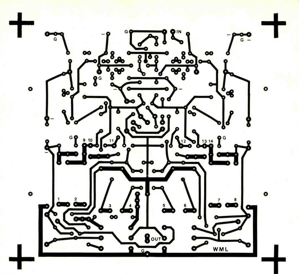
Fig. 12A.-Recommended circuit-board foil pattern for the copper foil or
circuit side.

Fig.128.-Recommended circuit-board foil pattern for the ground-plane or
component side.
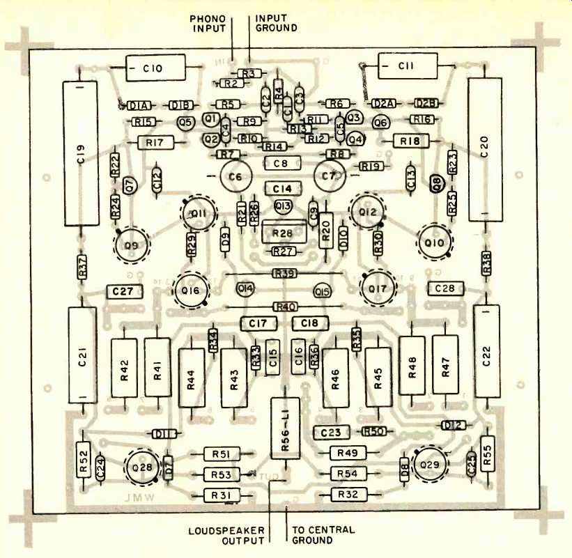
Fig. 13--Parts layout for the recommended foil pattern.
Circuit-Board and Heat-Sink Assembly
For optimum results, match the differential amplifier transistors for equal current gains at a collector-to-emitter voltage of 40 V. This will ensure freedom from d.c. offset problems at the loudspeaker output terminal caused by un equal base currents in the input-stage transistors. A simple test circuit can be constructed to match these transistors, as shown in Fig. 14. Optimally, Q1 through Q4 should have equal or nearly equal current gains. Should it be difficult to find a match for all four transistors, it is sufficient to match Q1 to Q3 and Q2 to Q4. A third combination is to match Q1 to Q2 and Q3 to Q4, but this is less desirable.
The first step is to solder six of the seven ground connections on the board; ground connections are marked with a G in Fig. 12A. The one which is not soldered at this point is the one nearest the loudspeaker output connection. To solder these connections, insert a 1/4-inch length of No. 22 solid wire through each hole and bend it down against the copper on each side of the board. On the ground plane side, it is best to bend these wires away from any adjacent component locations, especially those near capacitors C27 and C28. The connections can now be soldered. Sufficient heat must be used on the ground plane side to get a good solder joint-a good joint is one for which the solder has flowed smoothly onto the circuit board, and it appears shiny. Only a controlled heat soldering iron such as the Weller Soldering Station should be used to solder to the circuit boards. A 700-degree soldering tip is recommended, and the Weller PTM7 tip is an excellent choice. Only a high-quality solder such as Ersin SN62 multi-core No. 22 solder should be used. If difficulty is experienced in making the solder flow, use a pencil eraser to clean the area to be soldered and dip the tip of the solder into zinc chloride soldering paste before applying heat.
The next step is to mount and solder all 1/4-watt resistors, with the exception of R1, R58 and R59, to the board. All of these should be bent on a resistor bender for a 0.4-inch hole spacing, except for resistors R4, R39 and R40. These should be bent to 0.5 inch for R4 and 1.4 inch for R39 and R40. A 0.5-inch length of insulation should be inserted over each lead of the latter two resistors before bending them. When inserting the resistors into the board, extra care should be taken to prevent peeling off a metal burr from the solder-plated resistor leads which could short to the ground plane. If this hap pens, the burr should be removed with a small blade screw driver. Also, do not press the resistors down too hard against the ground plane, for their insulated coating could be broken and a short circuit could result.
With the exception of D3 through D6, the diodes should be installed next. They should be bent for a hole spacing of 0.4 inch and their proper direction is indicated by an arrow in Fig. 12B. The diodes should be installed such that the arrow points toward the banded end or cathode. All other resistors and capacitors should now be inserted. Each one-watt resistor should be bent for a 0.7-inch hole spacing. Pay particular attention to the polarity of the electrolytic capacitors. The negative terminals for these should be inserted into the holes labeled with a minus sign in Fig. 12B.
Next install all transistors which mount on the circuit board. The location of these transistors is labeled in Fig. 12A with the transistor number. Transistors Q1 through Q8 and Q13 through Q15 should be installed with their flat ends oriented as shown in Fig. 13. It is not necessary to bend the leads of these nine transistors to conform to the circuit-board hole spacings; simply spring the leads apart slightly and insert them until the transistors are about 5/16 inch off the board.
All TO-5 case, i.e. metal can, transistors that mount on the board should be installed so that they are about this same height above the board. All require clip-on heat sinks which should be installed on the transistors before they are soldered to the circuit boards to prevent bending the transistor leads. It is not necessary to use any heat sink compound on these transistors.
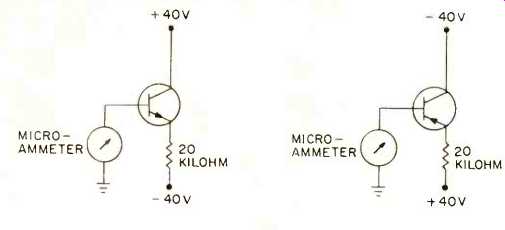
Fig. 14-Test circuits for matching transistors Q1 through Q4. Select transistors
for equal or nearly equal base currents. (A) Test circuit for matching
NPN transistors Q1 and Q2; (B) test circuit for matching PNP transistors
Q3 and Q4.
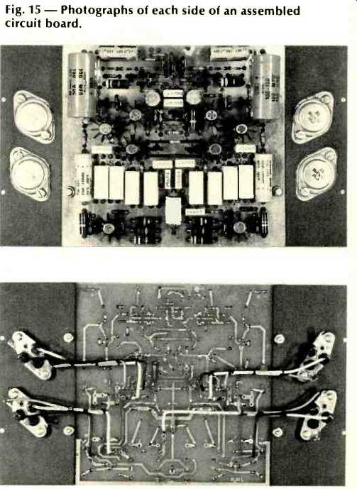
Fig. 15--Photographs of each side of an assembled circuit board.
The driver heat sinks can now be mounted to the circuit board as shown in Fig. 15. They are fabricated from 3/32-inch sheet aluminum, and the recommended dimensions are 5 1/2 x 21, inches. Mount them on the side of the circuit board opposite the ground plane with No. 4-40 x 3/8 inch screws with an inside star lockwasher under each nut. Insulate the driver heat sinks from the circuit board ground plane by installing a No. 4 fiber shoulder washer in each of the four mounting holes on the circuit board. The driver transistors can now be installed as shown in Fig. 15. A mica insulating wafer should be placed between each transistor and the heat sinks, and both sides of the mica wafers should be lightly coated with thermal compound. Use only molded plastic transistor sockets to install the drivers, and before connecting them to the circuit board, check with an ohmmeter for a possible collector short circuit to the heat sink or a short from a heat sink to the circuit board ground plane. If there are none, the driver leads can be connected and soldered as shown in Fig. 15; the connection codes are provided in Table I.
The final step in the circuit-board assembly is to solder the input coaxial cable, resistor R58, and the power supply, loudspeaker output, and power-supply ground leads to the board. With the exception of R58, these are all inserted from the side opposite the component side. Connect and solder appropriate lengths of color-coded No. 16 stranded wire to the plus and minus power-supply connections and to the loudspeaker output connection. To the ground connection nearest the loudspeaker output, insert one lead of resistor R58 over which 0.5-inch of insulation has been installed and one end of a length of No. 22 stranded wire. Solder these on both sides of the circuit board. Finally, connect and solder an appropriate length of miniature coaxial cable to the signal input and signal ground connections on the circuit board.
This completes the circuit-board assembly.
Preparation of the main heat sinks is the next step. If they are not predrilled, each must be drilled for four TO-3 transistors. To mark the holes, arrange four mica insulating wafers in each heat sink channel in the position of the transistors and use a pencil to mark the position of the four holes on each wafer. After tapping the marked positions with a sharp pointed punch, drill all holes with a /-inch bit on a drill press. Do not use a hand' drill. The holes must mate the transistors properly if short circuits to the heat sinks are to be avoided. In addition, each hole must be deburred to avoid a short circuit that could be caused by a punctured mica wafer.
After the output transistor holes are drilled, the heat sinks can be drilled for the bias regulator diodes. Two of these diodes mount in holes drilled in the center of each heat sink. Drill the holes about 3/8 inch apart with a diameter that permits the diodes to fit snugly without binding. Finally, the holes for mounting the circuit boards to the heat sinks and any holes necessary for mounting the heat sinks to the chassis must be drilled. The circuit-board mounting holes should be marked and drilled for No. 4 screws (No. 33 drill bit) in the heat-sink outer flanges to mate with the holes on the outer edges of the driver transistor heat sinks. These should be marked carefully to ensure proper fit of the circuit board assembly on the heat sinks. The method of mounting the heat sinks to the chassis may vary; I used bolts through the existing U-shaped cut-outs in the outer heat-sink flanges to attach aluminum brackets designed to hold the heat sinks 1/2 inch off the chassis bottom.
The output transistors can now be installed on the heat sinks. Use only high-quality molded plastic sockets. Because the heat sinks are so thick, it may be difficult to get a good connection between the socket pins and the base and emitter transistor leads. To solve this problem, I removed the pins from the transistor sockets and soldered them directly to the ends of the transistor leads. Care must be taken in positioning the pins on the transistor leads so that they will properly mate with the socket when installed on the heat sinks.
Although this increases the difficulty of replacing an output transistor in the event of a failure, it does ensure good electrical connections for the high-current output transistor leads.
The three wires to be soldered to the output transistor sockets should be color-coded No. 20 stranded wire about eight inches long. Next, install the transistors and sockets on the heat sinks. Each transistor should be insulated from the heat sink with a mica wafer that has been liberally coated on both sides with thermal compound. Transistors Q20, Q21, Q24, and Q25 mount on the heat sink that is to be closest to drivers Q18 and Q30, while Q22, Q23, Q26, and Q27 mount on the heat sink that will be closest to drivers Q19 and Q31.
Use an ohmmeter to verify that no transistor lead is shorted to the heat sinks.
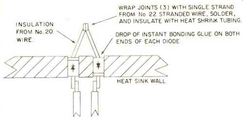
Fig. 16--Recommended mounting of bias diodes in each heat sink.
The diode bias assemblies are now installed into each heat sink and should be prepared as shown in Fig. 16. It is best to first solder the wire that is used to connect each diode to the circuit board, and these wires should be color-coded No. 22 stranded wire about eight inches in length. Before soldering, tie-wrap the joints with a single strand from No. 22 stranded wire to form a tight mechanical connection. After installation into the heat sinks, insulate the solder joints with heat-shrink tubing, preferably shrunk with a heat gun. Take extreme care to avoid cracking any of the bias diodes during installation into the heat sinks. If a crack occurs, the diode will become an open circuit and the amplifier can be seriously damaged.
Thus the diodes should not be forced into their mounting holes nor should there be tension on their leads. It is not necessary to use heat-sink compound on the diodes; if necessary, a drop of instant bonding glue on each may be used to bond them to the heat sinks.
Before attaching the circuit board to the heat sink, it is best to pretest it with a lab power supply. This can be done with dual 50-V supplies, preferably with a current-limit circuit. On the rear of the circuit board, temporarily tack-solder four 100-ohm 1/4-watt resistors, one from the emitter of Q30 to the collector of Q18, one from the emitter of Q31 to the collector of Q19, one from the emitter of Q18 to the junction of resistors R43 through R46, and one from the emitter of Q19 to this same junction. Solder a short-circuit jumper wire across C14.
With clip leads, connect the negative output of one power supply to the circuit-board ground wire and the positive output to the circuit-board positive power-supply input. Connect the positive output of the other power supply to the circuit-board ground wire and the negative output to the circuit-board negative power-supply input. With the power supplies set to current limit at 100 mA, the voltages can be slowly turned up. If current limiting does not occur or if the current drawn does not exceed about 50 mA, turn the power supplies off, use clip leads to connect the output of a signal generator to the signal-input cable, and connect an oscilloscope probe to the loudspeaker output wire. The oscilloscope ground should be connected to the circuit-board ground wire. With a sine wave of 1 V rms at 1 kHz applied to the input, slowly turn up the power supply voltages. A clipped sine wave that looks like a square wave should appear on the oscilloscope before reaching plus and minus 10 V. At 50 V, the sine wave will appear unclipped with an amplitude of about 60 V peak-to-peak. Turn the power-sup ply voltages down and connect a 10-kHz square wave source to the circuit-board input. With power supplied to the board, the output signal should look like the waveform of Fig. 8. If it does not, check the values of R3, R4, C1, C2, and C3.
If the previous tests are negative, the circuit board should be inspected thoroughly. Check for solder bridges; cold solder joints; shorted components to the ground plane; back ward electrolytic capacitors, transistors, and diodes; incorrect component values; unsoldered ground connections, etc. Correct all errors at this point--before the output transistors are connected. If components must be removed from the circuit board, desolder them with a desoldering braid (such as Solder Wick) and with as little heat as possible to prevent lifting the copper foil from the circuit board. When the circuit is operational, remove the jumper wire and four resistors from the rear of the board. The solder flux must now be removed from the boards with a soft-bristle brush and a good solvent (such as Stripper brand) spray-on circuit-board cleaner.
When cleaned, each solder joint will be shiny; dull joints may be cold solder joints so make sure they are touched up.
The circuit board is now ready to be mounted to the heat sinks. The wires from the power transistors and bias diodes should first be cut to length and soldered to the circuit board. These are connected from the circuit side of the board, i.e. the side opposite the components. To do this, lay the board in front of the heat-sink assembly with the ground plane side down and the loudspeaker output connection nearest the heat sinks. Cut the wires from the heat sinks just long enough so that after they are soldered to the board there will be no tension on them with the board in this position. If this is done properly, you will not have to desolder any wires from the board should it need servicing. However, to minimize undesirable coupling effects, the connecting wires should be no longer than necessary.
The proper connections of the wires from the heat sinks to the circuit board are given by the codes in Table I. After soldering these wires to the circuit board, use cable ties to separately tie the wires from each transistor and bias diode assembly into neat bundles. Carefully inspect the ground plane side of the board for any soldered wires that may protrude out too far and cause a short circuit. No wire should protrude through the board by more than 1/32 inch. When all wires are connected, double-check the wiring for errors.
The bias diodes especially should be checked for correct connection to the board, for backward diodes can damage the output transistors when the amplifier is first powered. The circuit board can now be attached to the heat sinks. This is done with four No. 4-40 x 1/4-inch threaded aluminum spacers and eight No. 4-40 x 3/8-inch screws with an inside star lockwasher under each. Neatly route the cabling between the heat sinks and circuit board after the circuit board is installed. This completes the circuit-board and heat-sink assembly.
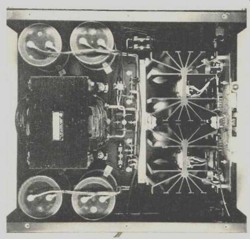
Fig. 17--Interior view of the amplifier chassis showing chassis wiring.
Wiring of the Chassis
The amplifier can be built on any chassis, provided the general layout and wiring used by the author are followed.
The chassis shown was bent from 16-gauge steel by a sheet-metal shop. Its dimensions are 17 inches W x 15 inches D x 6 1/4 inches H. A 7-inch x 19-inch steel panel is bolted to the front, and a perforated steel cover is placed over the chassis to make it mechanically rigid. The cover is screwed into No. 6-32 nutserts installed in the chassis outer flanges. An interior view of the chassis component placement and wiring is shown in Fig. 17. An aluminum chassis can be used, but it is difficult to paint and may not be strong enough to support the 38-pound transformer.
Before painting the chassis, punch and drill all holes, smooth sharp edges with a file, and remove all corrosion with a wire brush, sandpaper, and steel wool. For proper ventilation, vent the area beneath the heat sinks by punching eight 1 3/8-inch circular holes under the heat-sink assembly with a chassis punch. After the chassis is completed, thoroughly wash it with a spray-and-wipe all-purpose cleaner to remove oil traces. Next, prime and paint the chassis (I used Rust Oleum 960 spray primer and Rust-Oleum 7278 satin black spray paint). For best results, apply the paint in light duster coats and allow 30 to 60 seconds for the gloss to disappear between each spray. This will produce a professional-looking textured finish without runs. After one coat is built up, wait at least 48 hours before applying a second. This is important if the finish is to harden properly and not wrinkle.
The signal input jack must be insulated from the chassis, and a phono jack which mounts in a circular hole with a single nut from the back is recommended for this. It can be insulated from the chassis with a flat washer on one side and a shoulder washer on the other. The recommended loud speaker output connector is a double five-way binding post.
If two single five-way binding posts are used, drill the chassis for the standard 3/4-inch spacing between them.
Before placing the circuit-board and heat-sink assembly into the chassis, install the power supply and associated a.c. chassis wiring. The power supply is wired as shown in Fig. 2.
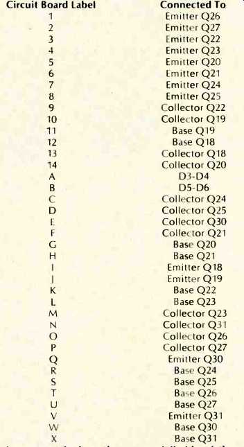
Table I--Codes for external connections to the circuit board. Numbers
are etched on the copper foil side of the circuit board and letters on
the ground plane side.
A single central chassis ground point is used, to which all high-current leads are connected. This central ground point should be a No. 10 machine screw on which are nine No. 10 soldering lugs separated by No. 10 flat washers. A No. 10 inside star lockwasher is installed under the bottom washer to ensure that the ground point makes good connection with the chassis ground through the paint. Firmly tighten the screw so that these lockwashers engage properly. The green a.c. safety ground from the power cord, the filter capacitor grounds, and the two transformer center taps are then connected to the ground point. The circuit board ground wire and the loudspeaker output ground terminal are also connected to this point after the circuit-board and heat-sink assembly has been installed. The latter connection should be made with a length of No. 16 stranded wire. It is important to carefully solder all the high-current leads in the power sup ply. Also, the central ground point must make good electrical connection to the chassis. Before mounting the transformer, clean all paint and corrosion from its terminals, coat them lightly with zinc chloride soldering paste, and in stall a 1/4-inch screw-size grommet into each hole in the transformer mounting brackets. The transformer is installed with four 1/4-20 x 3/4-inch bolts with two No. 10 flat washers between each grommet and the chassis--one washer between each grommet and nut, and one washer under the head of each bolt. Solder separate lengths of No. 16 stranded wire from the two secondary terminals labeled 57 1/2 V to the central ground point. Next, solder separate lengths of No. 16 stranded wire from the two terminals labeled 0 V to one a.c. input on the bridge rectifier. Similarly, solder No. 16 wire from the terminals labeled 115 V to the other a.c. input on the bridge rectifier. Solder capacitor C29 directly across the two a.c. inputs on the rectifier. Wire the d.c. outputs from the bridge rectifier to a terminal strip from which separate lengths of No. 16 stranded wire are connected to each filter capacitor and to the d.c. power-supply fuse clips. The three wires on the a.c. power cord must be connected properly to minimize shock hazard. First, coat each lead with zinc chloride soldering paste and solder the leads to separate terminals on a terminal strip. Solder a length of No. 18 stranded wire from the terminal with the green or safety ground wire to the central ground point. Next, solder a length of No. 16 stranded wire from the white or neutral wire to the 0-V transformer primary tap. The black or "hot" power-cord wire should be connected with lengths of No. 16 stranded wire through the a.c. fuse clip and the a.c. power switch to the 115-V transformer primary tap. The pilot light is connected in parallel with the transformer primary.
After the power supply has been wired, the heat-sink and circuit-board assembly can be mounted on the chassis and connected to the power-supply fuse clips, the central ground point, and the loudspeaker output terminal. The No. 16 and 22 stranded wires for these connections should already have been soldered to the circuit board. Before soldering leads to the loudspeaker output terminals, install the series combination of resistor R57 and capacitor C26 directly across the terminals and connect one end of resistor R59 to the loudspeaker ground terminal. Solder the other end of this resistor to a nearby grounding solder lug. The loudspeaker output wire from the circuit board and the speaker ground wire from the central ground point can now be connected and all connections soldered. Next, solder the free end of resistor R58 to a grounding solder lug that connects to the chassis ground ,near the circuit board ground (to which this resistor connects). The final step is to connect the input leads to the phono input jack. Solder resistor R1 between the insulated phono jack ground and a nearby grounding solder lug.
Proper grounding is a must if ground loop problems are to be avoided. To minimize these problems, separate chassis and signal grounds were used. The circuit-board ground plane was insulated from the driver transistor heat sinks so that there is only one direct connection between the circuit-board ground and the central ground point-through the wire soldered to the ground connection nearest the loudspeaker output connection on the circuit board. There are three small value resistors that complete the grounding--R1, R58, and R59. Resistor R1 solders between the insulated ground terminal on the phono input jack to a solder lug connected to the chassis ground adjacent to the jack. Resistor R59 solders between the loudspeaker output ground terminal and a solder lug connected to the chassis ground adjacent to the loudspeaker output terminal. Resistor R58 solders between the circuit-board ground closest to the loudspeaker output connection to a nearby grounding solder lug. Al though complicated, this grounding procedure follows the practices recommended in [161 and should ensure freedom from oscillations and hum that can be caused by mutual coupling in the ground system.
These steps complete the amplifier assembly.
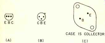
Fig. 18--Transistor pin connections. Views are from the pin side of each
transistor. (A) Small signal plastic case transistors; (B) TO-S metal case
transistors, and (C) TO-3 metal case transistors.
Turn-On Procedure
Before attempting to apply power to the amplifier, it is strongly recommended that the entire unit be checked for errors. If everything appears to be correct, the initial tests can be performed. First, install the a.c. power fuse; do not install the d.c. power fuses to the circuit board at this point. Plug the a.c. power cord into a Variac autotransformer, turn the amplifier on, and slowly increase the a.c. voltage until a d.c. voltage of about 5 V is measured with a voltmeter across the d.c. outputs of the bridge rectifier. The polarity of the voltages on each filter capacitor should now be checked with the voltmeter before increasing the voltage further. If the voltage polarity is incorrect on any capacitor, it will short-circuit if the voltage is increased. If all filter capacitors are polarized correctly, the a.c. voltage can be increased to 120 V.
Do not increase the Variac above that value. The positive and negative d.c. power supplies should read within one or two volts of 85 V. The a.c. power can now be removed. Before further tests, discharge the filter capacitors with care, since approximately 110 joules of energy will be stored in them. It is best to do this by connecting two leads to a 16-ohm dummy speaker-load box and then touching the leads across the terminals of each capacitor for several seconds. If a dummy load box is not available, a 3.9-kilohm, 2-watt resistor can be used although the discharge will take several minutes. Do not hold a resistor by its body across the capacitor terminals to discharge them, for the resistor can become hot enough to burn the fingers.
In the next test, d.c. power is applied to the circuit board.
Before proceeding, adjust potentiometer R28 for maximum resistance, i.e. 5 kilohms. This should be verified with an ohmmeter, for otherwise the power transistors could be damaged in the next test. Install a 10-ohm, 2-watt resistor with clip leads across each d.c. fuse clip to prevent the release of excessive current into the circuit if there is an error. If every thing is normal, the current through the resistors in the next test will be less than 50 mA and the voltage drop across them negligible. Apply a 1-kHz sine-wave signal of amplitude 1 V rms to the amplifier input. With an oscilloscope, check the signal at the phono input jack to ensure there are no short circuits in the input cable from the jack to the circuit board.
If there are no shorts, connect the oscilloscope to the loudspeaker output terminals. With the a.c. power switch on, slowly increase the a.c. voltage with the Variac until the output signal is observed. The signal will initially appear as a clipped sine wave that looks like a square wave. If no problems are encountered, the a.c. voltage can be slowly increased to 120 V. The amplitude of the sine wave output signal should be about 60 V peak-to-peak. The input signal should now be removed and the d.c. output voltage from the amplifier measured. This should be less than 100 mV, al though a slightly higher value is acceptable. The magnitude of the d.c. offset depends on the matching of the transistors in the differential amplifiers, i.e. Q1 through Q4.
If the preceding tests are successful, the bias potentiometer R28 can be adjusted next. Remove the a.c. power and discharge the power-supply capacitors. Install a fuse in the negative power-supply fuse clip and a d.c. milliammeter across the positive power-supply fuse clip. With no input signal and no load connected to the loudspeaker output terminals, slowly turn the Variac up until the a.c. input voltage is 120 V. Adjust R28 until the milliammeter reads 250 mA. This will bias the amplifier so that it operates Class-A for a peak power level of 2 W or less with an 8-ohm load, thus eliminating all traces of crossover distortion. Let the amplifier idle for at least 30 minutes while readjusting R28 for 250 mA every few minutes. When the current stabilizes to this value, the heat sinks will be warm to the touch.
The amplifier is now ready to be used. Turn it off and let the power supply discharge. When the milliammeter reading drops to zero, remove it from the fuse clip and install the positive power-supply fuse. The amplifier will have no turn on thump if it is switched on after the power supply has completely discharged. This takes several minutes after each turn-off. To prevent turn-on thumps from the preamplifier from reaching the loudspeaker, always turn the preamplifier on for several seconds before turning on the power amplifier, and always turn the power amplifier off and wait until the sound stops before turning off the preamplifier. This procedure should always be used with d.c.-coupled amplifiers to prevent d.c. transients generated in the preamplifier from reaching the loudspeakers.
Concluding Comments
The basic circuit topology of the amplifier was originally conceived in 1975. With the enormous tasks of completing the circuit design details, translating them into a finished amplifier, and describing its construction for this article accomplished, the task of building a second amplifier to complete a stereo system will begin.
The original intent was to build a single stereo amplifier rather than two mono units. However, I recognized that most audiophiles who build the amplifier would probably prefer the two channels with separate power supplies. Thus, weight and size limitations dictated a separate chassis for each channel. A single chassis and power supply can be used if desired, although a special grounding procedure must be observed to prevent hum caused by ground loop problems. The two pho no input jacks should be installed adjacent to each other.
Connect their insulated grounds together and use a single resistor R1 from this connection to a nearby grounding solder lug. Omit the No. 22 ground wire that connects from the circuit-board ground of one channel back to the central ground. This circuit board will then be grounded back through the phono input cable grounds, the circuit-board ground plane of the other channel, and the No. 22 wire which connects that channel to the central ground point.
Resistors R58 and R59 should be installed on both channels as described previously.
The problem of obtaining parts is not a trivial one. The transistors and diodes cannot be bought from consumer electronics stores or those that supply TV repair shops; they can only be ordered through industrial electronics suppliers.
Under no conditions should substitute transistors or diodes be used, for the amplifier is frequency-compensated only for the types and manufacturers specified in the parts list. Many parts, such as heat sinks and filter capacitors, can be obtained from money-saving mail-order electronics surplus companies. There are also many mail-order firms that sell high-quality non-surplus items such as carbon film resistors, small electrolytic capacitors, small signal transistors, zener diodes, chassis hardware, etc. at bargain prices. The addresses of these companies can be found in the back pages of many consumer electronics magazines. (A list of sources for parts will be sent with all circuit board orders from the supplier listed in the accompanying parts list.) The power transformer is the single most expensive item in the amplifier. If two surplus 230- to 115-V transformers can be found, their primaries can be connected in parallel and secondaries in series to form a 115- to 115-V transformer. If the transformers are not connected properly, the series secondaries will be out of phase and the voltages will cancel.
Therefore, an a.c. voltmeter should be used to verify that the secondaries are phased properly. The current rating of the 115-V windings should be no less than 10 A. The specified transformer has a current rating of 12 A with its two 6-A secondaries connected in parallel for a 115 to 115-V rating.
One measure of transformer quality is the weight. The specified one weighs 38 pounds, which should be comparable to the total weight of any substitute transformers. Under no conditions should more than 85 V be used on the amplifier power supply. With substitute transformers, it is sometimes possible to remove several turns from the secondary to re duce the output voltage in case it is too high. If the line voltage runs higher than 120 V a.c. with the specified transformer, the 125-V primary tap should be used. If a 230 W amplifier is sufficient, the use of the 125-V tap is highly recommended. This will ensure protection of the amplifier in case the a.c. line voltage increases due to poor regulation by the power company. With a line voltage of 120 V a.c., the power supply voltages will be plus and minus 80V.
Removal of the Bessel input filter to increase the amplifier bandwidth beyond 40 kHz is not recommended, for the frequency compensation will be affected. Capacitor C1 in this filter affects the high-frequency bandwidth of the input stage for signals applied to the feedback input. Its removal may cause oscillations. Also, because the amplifier slew rate is so high, the filter protects the amplifier and its loudspeaker load from accidental or unintentional ultrasonic input signals.
Some advertisements have misled audiophiles to believe that very wide bandwidths are required for negligible phase distortion. Thus, some builders may be tempted to remove the filter to extend the amplifier bandwidth to 500 kHz. Do not do this, for the circuit still has a bandwidth of 500 kHz with the filter. The filter simply prevents signals with a frequency higher than 40 kHz from entering the circuit. The phase response of the Bessel filter has been carefully researched [3].
The filter phase response is such that it introduces a constant time delay in the audio band of 5.4 uS. This delay is equivalent to the listener moving 1/16 inch back from the loudspeaker. Further, it is minuscule compared to the time delay between an original recording session and any play back of the recording. As a point of interest, the nice phase characteristics of a Bessel low-pass filter are not shared by a Bessel high-pass filter. Thus, unfortunately, the low-frequency phase response of loudspeakers cannot be successfully linearized with the Bessel alignment.
As stated previously, removal of the limiter circuit is not recommended. Its threshold is high enough so that it would not be triggered by normal loudspeaker loads. Also, the limiter circuit will not respond to fast transients so that it will not limit the slew rate of the amplifier with normal loads.
Without the limiter, an accidental short circuit on the loudspeaker output can severely damage the amplifier, and I have heard from several builders of the low TIM amplifier [4], [5] who related their unfortunate experiences. In one case, the builder lost his amplifier when he sat on the bed; investigation showed that the loudspeaker wire ran under the carpet and beneath the bedpost.
Finally, there are some precautions which should be ob served in testing the amplifier. Never attempt to apply continuous large-amplitude high-frequency sine waves or square waves to the input. Not only could the output transistors be damaged, but resistor R57 will surely be fried. This resistor must be noninductive, and thus a carbon composition resistor is specified. The highest wattage standard carbon-composition resistor is 2 W. If the amplifier is tested at 20 kHz with a full power sine wave, it will dissipate 3 W. With a square wave, it would be about double this figure. If the builder anticipates that the amplifier will be subject to continuous sine or square wave tests that could fry R57, it is recommended that four 39-ohm 2-W resistors be connected in parallel to form this resistor, which will increase its power rating to 8 W.
During any tests, occasionally touch these resistors to check that they are not so hot that they could be damaged. With normal audio signals, R57 is safe at 2 W. If R57 is unknowingly fried during a test, the stability of the amplifier with reactive loads could be affected. This means that it may oscillate with reactive loads and possibly damage the output transistors.
For those readers who wish to ask questions or make comments about this construction article, I ask that you please not use the telephone. I must politely refuse all calls made to my office at Georgia Tech that pertain to this type of project.
Instead, mail letters to me and enclose a self-addressed stamped envelope for return; I will make every effort to answer them. I sincerely hope that the ideas I have expressed in this article will spark the imagination of readers, and I wish the best of luck to those who build the amplifier. The best advice I can offer is to take your time! It has taken me four years to build my amplifier, and I estimate that anyone who takes less than four months to acquire the parts and build it will do a sloppy job. Happy listening!
Addendum
Although not indicated on the circuit diagram, parts list, or parts layout, the protection circuit should be modified by the addition of two diodes and two resistors. The diodes should be type 1N4934. The resistors should be 680-ohm 1/4 W 5 percent. Solder one diode and one resistor in parallel across the leads of capacitor C17 and the other diode and resistor in parallel across the leads of capacitor C18. The banded end or cathode of the diode which connects in parallel with C17 should be the end that connects back to the center lead or base of transistor Q14. The unbanded end or anode of the diode which connects in parallel with C18 should be the end that connects back to the center lead or base of transistor Q15. If the diodes are installed backward, the operation of the protection circuit will be seriously affected.
---------------
Parts List
All resistors are 1/4-W 5 percent carbon film unless otherwise specified. Manufacturer codes for active devices: M-
Motorola, R-RCA, I-ITT, N-National Semiconductor. Do not substitute transistor or diode types or manufacturers.
R1-4.7 ohm.
R2-43 kilohm.
R3, R4-6.2 kilohm.
R5 through R12 and R29, R30-270 ohm.
R13, R14-10 kilohm.
R15, R16-1.2 kilohm.
R17, R18-4.3 kilohm, 1 W.
R19, R40-240 ohm.
R20, R52, R53, R54, R55-5.6 kilohm, 1 W.
R21-56 kilohm.
R22, R23-20 ohm.
R24, R25-330 ohm.
R26, R27-1 kilohm.
R28-5 kilohm trimpot (CTS X201R).
R31, R32-3.9 kilohm, 1 W.
R33, R34, R35, R36-360 ohm.
R37, R38-100 ohm.
R39-470 ohm.
R41 through R48-0.22 ohm, 5 W.
R49, R51-15 kilohm, 1 W.
R50-39 ohm.
R56-10 ohm, 2 W.
R57-10 ohm, 2 W or four 39-ohm, 2 W resistors in parallel (see text).
R58-3.3 ohm.
R59-1 ohm, 1/2 W.
C1-430 pF silver mica (Arco DM15-431J).
C2, C3, C24, C25-270 pF silver mica (Arco DM15-271J).
C4, C5-15 pF silver mica (Arco DM15-150J).
C6, C7-330 uF, 10-V radial electrolytic (Panasonic 330/10R).
C8, C14, C17, C18, C26, C27, C28-0.1 uF, 100- or 250-V metallized polyester (Plessey Minibox 0.1/100 or 0.1/250, C or D box).
C9-15 pF silver mica (Arco DM15-150j).
C10, C11-100 uF, 50-V axial electrolytic (Panasonic 100/ 50A).
C12, C13-10 pF silver mica (Arco DM15-100J).
C15, C16, C23-0.01 uF, 400- or 630-V metallized polyester (Plessey Minibox 0.01/400 or 0.01/630, B or C box).
C19, C20-100 uF, 100-V axial electrolytic (Mallory TC10101B).
C21, C22-25 uF, 100-V axial electrolytic (Mallory TC10250C).
C29-0.1 uF, 250-V metallized polyester (Panasonic 104K).
C30-0.01 uF, 630-V metallized polyester (Plessey Minibox 0.01/630, C box).
C31, C32, C33, C34-8,600 uF, 100-V electrolytic (Mallory CG832U100G1).
11-10 turns No. 22 solid insulated wire wound tightly around R56 and soldered to the resistor leads.
D1, D2-Two 1N5250B 20-V zener diodes in series for each.
D3, D4, D5, D6-1 N4001, 1N4002, 1N4003, or 1N4004.
D7, D8, D9, D10--1N4934 (M) fast recovery rectifier.
D11, D12-1 N4935 (M) fast recovery rectifier.
Rect 1--MDA3504 (M) 400-V, 35-A bridge rectifier.
Q1, Q2, Q5, Q8, Q13, Q14--MPS8099 (M) or 2N5210 (M, I, or N).
Q3, Q4, Q6, Q7, Q15--MPS8599 (M) or 2N5087 (M, I, or N).
Q9, Q11, Q17, Q29- MM5415 (M) or 2N5415 (R).
Q10, Q12, Q16, Q28-2N3439 (M or R).
Q18, Q30-MJ15001 (M).
Q19, Q31--MJ15002 (M).
Q20, Q21, Q24, Q25--MJ15003 (M).
Q22, Q23, Q26, Q27-M115004 (M).
T1--Signal transformer 230-6, 115V C.T., 12A (Signal Transformer, 500 Bayview Ave., Inwood, N.Y. 11696).
F1, F2--8-A 3AG fast blow fuse (Littlefuse 312008).
F3--6.25-A, 3AG slow blow fuse (Littlefuse 3136.25).
S1--15-A 125 VAC two-pole single-throw circuit breaker (Airpax T21-2-15.0A-01031) with both poles wired in parallel, punch chassis for 1/2-in. hole.
One neon pilot lamp (Drake 6063-001-634), drill chassis for 3/8-in. hole.
One etched, plated, and drilled ground plane circuit board (see text).
Two heat sinks to mount on circuit boards for Q18, Q19, Q30, Q31 (see text).
One three-conductor UL-type Si No. 16 a.c. line cord (Alpha 618) and line cord strain relief (Heyco SR-6P3-4), punch chassis for 5/8-in. hole.
One phono chassis jack (Switchcraft 3505F) insulated from chassis with 3/4-in. I.D. nylon shoulder washer on one side and flat nylon washer on other, punch chassis for 1/2-in. hole.
One double five-way binding post (Superior Electric DF30-2 BRC) for loudspeaker output terminals.
Three 3AG fuse mounting holders (Littlefuse 357001).
Four 4-40 x 1/4 in. x 1/4 in. O.D. aluminum threaded round spacers (Waldom 60477) for mounting circuit board to heat sinks.
Twelve TO-3 transistor sockets, molded types preferable.
Twelve TO-3 mica insulating wafers.
Eight TO-5 transistor finned heat-sink coolers ( Wakefield 205CB).
Two Wakefield 441K transistor heat-sink coolers drilled for Q20 through Q27 and D3 through D6 (see text).
Misc.--Suitable heavy-duty steel chassis with cover; mounting brackets for circuit board and heat-sink assembly; silicone heat-sink compound; shielded phono cable; No. 16, 18, 20, and 22 stranded hook-up wire; No. 22 solid hook-up wire; five heavy duty Y2-in. hard plastic feet; No. 6 and No. 10 soldering lugs; chassis hardware; rubber grommets for mounting transformer; etc.
An etched, drilled, and reflow solder-plated circuit board plus two mating heat sinks punched for the four driver transistors are available for $16 from Custom Components, P.O. Box 33193, Decatur, Ga. 30033. Shipping and handling charges for orders inside the continental USA are $1.00 plus five percent of the total price of each order. Georgia residents must add four-percent sales tax.
(adapted from Audio magazine, May. 1980)
Also see:
Build a Class-A Amplifier (by Nelson Pass) (Feb. 1977)
Construct a Wide Bandwidth Preamplifier (Feb. 1977)
Transient IM Distortion in Power Amplifiers (Feb. 1975)
Trends for the Future (April 1980)
= = = =