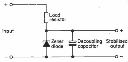
Fig. 8 A zener shunt stabilizer circuit.
| Home | Audio mag. | Stereo Review mag. | High Fidelity mag. | AE/AA mag. |
There are many applications where the variations in supply voltage associated with un-stabilized supplies would result in the equipment giving inconsistent results, or where damage could even be inflicted on the supplied equipment, as exprain41 in the previous section. There are also a number of applications where a very well smoothed supply is required, and a stabilized supply is of advantage here because the regulator circuit counteracts all variations in the output potential, including ripple.
In this section we shall be concerned with stabilized supplies that provide a single voltage, and are primarily intended for use as a permanent part of some larger piece of equipment. Variable voltage stabilized supplies, primarily intended-for use as bench power supplies, will be dealt with in the subsequent section.
Zener Stabilization
The most simple form of voltage regulator is the zener shunt stabilizer, and this uses the very simple circuit shown in Figure 8. The zener diode has a voltage rating which is equal to the required output voltage, or the nearest preferred value to the desired voltage if there is no preferred value giving the correct voltage.
At voltages below its rated voltage a zener diode has a very high resistance, usually many megohms. If the applied voltage is taken above the rated voltage, or 'zener voltage' as it is more commonly known, the resistance of the device drops considerably. In fact, raising the applied voltage to only a fraction of a volt above the zener voltage may well cause the effective resistance of the device to fall to just a few ohms.
Fig. 8 A zener shunt stabilizer circuit.
The input voltage must, of course, be somewhat higher than the stabilized output voltage. The zener diode then 'avalanches' it to conduction, causing a voltage drop across the load resistor and producing an output voltage approximately equal to its zener voltage. Increasing the input voltage causes the zener diode to conduct more heavily, causing a higher current to flow and the voltage dropped across the load resistor to increase. This results in the output voltage only marginally increasing. Conversely, if the input voltage decreases, the zener diode conducts less heavily, a lower current flow is produced, and the voltage drop across the load resistor decreases. This gives only a marginal drop in the output voltage.
The circuit not only guards against variations in the input potential, but prevents output loading (within reason) from producing large variations in the output voltage. For example, if there is an increase in the output current, this tends to reduce the output voltage, and the zener conducts less heavily.
Thus, although the increased output current raises the voltage drop across the load resistor, this is largely offset by the zener conducting less heavily, and only a slight reduction in the output voltage actually occurs.
One problem with a zener diode is that when used in this way it tends to generate a certain amount of noise, and it does so over a very wide bandwidth. In fact zener diodes are some times employed in noise generators. This will not always be of any importance, but in many applications it is necessary to add a decoupling capacitor across the zener in order to severely attenuate this noise. In mains power supplies the addition of this capacitor, together with the load resistor, gives additional smoothing. The stabilization effect of the zener diode also gives smoothing of the supply.
Low Voltage Zeners
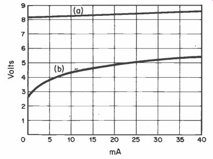
Fig. 9 Performance curves for (a) a typical 8.2V zener, and (b) a typical
3.9V type.
Most zener diodes give excellent regulation performance in practice, but the performance of most lower voltage types is usually markedly inferior to the high voltage components. It is devices having voltage ratings below about 6.2 volts that have a lower level of performance, as can be seen by referring to the two graphs shown in Figure 9. These show the zener voltage versus zener current for a 3.9V and a 8.2V device.
As can be seen from these, the voltage across the 8.2V type does not vary a great deal, and increases in proportion to the zener current producing a straight line on the graph. The response for the 3.9V type is reasonably flat at zener currents of about to 25 to 40 mA. but is very steep at currents of between zero and a few mA, giving very mediocre performance.
Therefore, in highly critical applications it is better not to use a low voltage tenet, unless only fairly small variation, in the zener currents are likely to occur.
Zener Ratings
There are three principal ratings for zener diodes: zener voltage, the error tolerance of the zener voltage, and the maximum permissible power dissipation.
As the zener voltage does vary somewhat with the current flowing through the device, it must be given at some particular current. For the popular BZY88 series of miters, for instance, the zener voltage is specified at a current of 0.5 mA. Naturally the teller voltage will not be precisely the specified figure, and for the BZY88 series of devices it will be within 5% of the rated voltage (at a zener current of 5mA). The maximum power dissipation figure is really self explanatory, and is 400 mW for the BZY88 series of zeners. Higher power types such as the BZX61 series (which have a 1.3 watt maximum permissible dissipation) are available, but very high power types seem to be no longer generally available.
The reason for this is that zener shunt stabilizers are not very efficient, since there is always a high current drain on the power source even when little or no current is being drawn from the supply. In low power applications, whether the power source is a battery or a mains transformer, efficiency is rarely of any great consequence. In high power circuits a terser shunt stabilizer can lead to rather short battery life in battery powered equipment, and the generation of unnecessarily large amounts of heat whatever the power source.
It is therefore recommended that the use of zener shunt stabilizers should be restricted to low power applications. For higher power circuits it is usually better to use a series regulator, and these will be covered later in this section.
Zener Polarity
The zener diode must be connected with the polarity shown in Figure 8 if it is to function correctly. If the input and output supply polarities are reversed, then the polarity of the zener must also be reversed (as must the polarity of the decoupling capacitor) for the circuit to operate properly. If the zener is connected the wrong way around it is then merely an ordinary forward biased silicon diode, and effectively produces a zener voltage of about 0.7 volts (actually fractionally more than most silicon diodes).
The fact that a forward biased silicon diode acts as a very low voltage zener can, and often is, put to good use. Zener diodes having voltages below about 2.7 volts are not generally available.
and so some alternative is needed for lower voltages. A forward biased silicon diode, or several in series is a simple and inexpensive method of obtaining very low stabilized potentials.
For example, if a stabilized supply of 2 volts is needed. the basic circuit configuration of Figure 10 can be used. Here there are three silicon diodes in series which effectively form a zener diode. There is about 0.65 volts developed across each diode, giving a total zener voltage of approximately 1.95 volts.
This should be close enough to the required figure of 2 volts for the majority of applications.
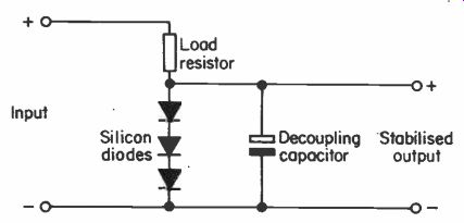
Fig. 10. A shunt stabilizer using forward biased silicon diodes.
Amplified Diode
Another form of low voltage regulator is the 'amplified diode' arrangement shown in Figure 11. If we, assume that R1 and R2 have the same value, the circuit will provide a zener voltage of about 1.2 or 1.3 volts. This is because about 0.6 to 0.65 volts is required at the base of Tr1 in order to switch the device on. and a marginally higher voltage is all that is needed in order to bias the device hard into conduction. The voltage at the output therefore rises to about 1.2 or 1.3 volts, whereupon Tr1 conducts heavily and prevents any significant further rise in voltage. The circuit thus provides an effect which is similar to a zener diode.
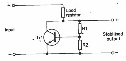
Fig. 11 Shunt stabilizer using an 'amplified' diode.
However, one important property of this form of regulator is that within reason, any desired output voltage can be obtained. For example, reducing the value of R2 increases the voltage drop across the potential divider circuit and increases the voltage needed at Tr1's collector before the device switches on (and therefore increases the effective zener voltage). Decreasing the value of R1 has the opposite effect, reducing the voltage drop through the potential divider and decreasing the effective zener voltage of the circuit.
The zener voltage is approximately equal to:
0.65 (R1 + R2)/R2
An important asset of this configuration is that the potential divider can be formed by a preset potentiometer, and the output voltage is then adjustable from about 0.65 volts up to about 6 volts or so. The performance, of the circuit falls off as the output voltage increases, due to the decreased level of feedback caused by increased losses through the potential divider. It is therefore not advisable to use this configuration for voltages of more than about 6 volts.
For best results a high gain transistor should be used, such as a BC109C, BC169C, BC650 or similar. A p.n.p. device can be used, but the input polarity must be reversed. RI and R2 should not be so high in value that they do not provide a reasonably large base current for Tr1, but not be so low as to prevent an adequate output voltage being obtained by producing an excessive voltage drop across the load resistor. The total resistance through the load resistor is usually about ten times the load resistance value.
The performance of silicon diode stabilizers and amplified diode regulators is normally very good, and superior to that obtained from low voltage zener diodes. One slight problem is that the temperature stability of these circuits is not quite as good as can be attained using a zener diode. However, the voltage change from silicon diodes and amplified diodes is only about 0.3 to 0.4% per degree Celsius, and is not a problem in the majority of applications.
Load Resistor Value
Whatever form of shunt regulator is used, the load resistor must have a low enough resistance to provide the required output current when the input voltage is at its minimum level. For example, if a 5.6 volt zener is fed from a 9 volt battery supply, and a maximum output current of 10mA is required, a load resistor of 190 ohms in value is required. This is because the output voltage from a 9 volt battery that is nearing exhaustion but is still in a useable state is only about 7.5 volts, and with 5.6 volts across the zener this only leaves about 1.9 volts across the load resistor. From Ohm's Law we know that resistance equals voltage divided by current, which gives us 1.9 volt:, divided by 0.01 amps (10 mA), which equals 190 ohms.
To allow for component tolerances a slightly lower value would be used in practice. say 180 ohms or preferably 150 ohms.
With a new battery connected to the circuit there will be a supply voltage of about 9.5 volts, giving about 3.9 volts across the load resistor and a current flow of 22 mA (180 ohm load resistor) or 26 mA (150 ohm load resistor). The power dissipation in the zener diode is therefore only about 145.6 mW (5.6 volts x 0.026 amps = 0.1456 watts or 145 mW) even with the lower load resistor value, and so a small zener such as a BZY88C5V6 400 mW type is perfectly suitable.
The maximum power dissipation in the load resistor is only about 101.4 mW (3.9 volts x 0.026A = 0.1014 watts or 101.4 mW) even if it has the lower value of 150 ohms, and so even a miniature 1/8 watt type could be used here, although it would be advisable to use a more conservatively rated component in the interests of long term reliability.
Series Regulators
A series regulator is one where the input current is little higher than the output current, the difference between the two currents being the small amount drawn by the regulator itself.
In effect, a series regulator is a variable resistance connected into one supply rail, with the resistance automatically adjusting itself to whatever value is needed in order to maintain the output voltage at the appropriate level. Its main advantage over a shunt type regulator is its high efficiency, resulting in a minimum of wasted power and heat generation. For this reason, series regulators are normally used in all applications, except where very low powers are involved, and efficiency and heat generation are not of any great importance.
In its simplest form a series regulator can merely consist of a zener shunt regulator feeding an emitter follower buffer stage, as shown in Figure 12. There is unity voltage gain through an emitter follower stage, and so by applying a stabilized input to the base, a stabilized output is obtained from the emitter. As the transistor provides current gain, the output current from the emitter can be far higher than the input current to the base. Thus, with a current flow of about 1 or 2 mA in the zene shunt stabilizer circuit, and a quiescent current consumption of the same level of course, an output current of perhaps 100 mA or more would be available at the output. The input current is equal to the output current plus the 1 or 2 mA drawn by the zener stabilizer, and so quite good efficiency is attained.
Input ; Zener Decoupling diode capacitor
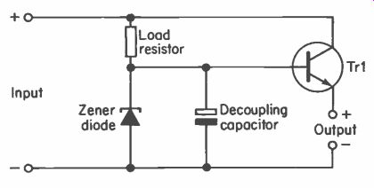
Fig. 12 A simple series regulator circuit.
Output
Provided the input voltage to the circuit is not inadequate to give the desired output voltage, the voltage at the output is virtually independent of the input voltage, and is controlled by the base voltage of Tr1. The zener diode and decoupling capacitor produce a very well smoothed voltage at Tr1's base, and this is reflected in an output which is almost equally free from noise. This enables circuits of this type to produce outputs having very low ripple and noise contents without the use of especially large smoothing capacitors, even at output currents as high as 1 amp or more. Output noise levels of about 1 mV maximum are quite typical for power supplies of this general type, and noise levels of just a few tens of microvolts can be readily attained.
The output voltage from a circuit of this type is not equal to the zener voltage, since there is a voltage drop of about 0.65 volts between the base and emitter terminals of Tr1. This drop must therefore be subtracted from the zener voltage in order to give the nominal output voltage of the circuit. This voltage drop assumes that the output impedance of the emitter follower stage is very low in comparison to the load impedance.
In other words, the current in the zener stabilizer circuits multiplied by the current gain of the transistor should give an answer that is far higher than the maximum output current.
The regulation of this type of circuit can never be equal to the regulation of the zener circuit, since the emitter follower cannot have zero output impedance, and the voltage drop through the stage must increase slightly with increasing output current. However, good regulation will be obtained if the zener current multiplied by the current gain of the transistor is at least one hundred times the required maximum output current.
In practice this usually means that two or even three transistors must be used in order to obtain sufficient gain. A basic two transistor circuit using an emitter follower Darlington pair is shown in Figure 13(a) and Figure 13(b) shows the method of using three transistors in a Darlington-emitter follower circuit.
Note that using two transistors results in an increased voltage drop of about 1.3 volts from the base of the first transistor to the output, since approximately 0.65 volts is dropped across each transistor. For a three transistor circuit this means a voltage drop of just under 2 volts from the base of the first transistor to the output.
An arrangement which is occasionally encountered is one where two common emitter amplifiers with 100% overall negative feedback are used. This arrangement is shown in Figure 14.
Although common emitter stages normally have a high level of voltage gain, this is not the case here due to the 100% negative feedback which is applied from the collector of the output transistor to the emitter of the driver transistor. This gives the amplifier a gain of almost exactly unity.
(a) A series regulator using a Darlington pair.
(b) A series regulator using a triple Darlington arrangement.
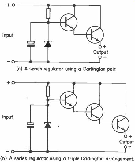
Fig. 13.
An advantage of this arrangement over a Darlington Pair emitter follower circuit is its lower voltage drop from the input to the output. The voltage drop through this type of circuit is only about 0.65 volts, permitting higher efficiency, and enabling the circuit to function properly even if the un-stabilized input voltage is only a few hundred millivolts higher than the required output voltage.
All the configurations shown in Figures 12 to 14 can be made to operate with a positive earth rail, but the polarity of the zener must be reversed, n.p.n. transistors should be changed to...
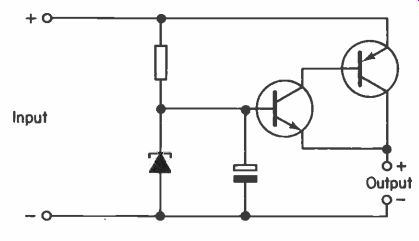
Fig. 14 A common emitter series regulator stage.
... p.n.p. types, and p.n.p. devices should be altered to n.p.n. types.
Battery Eliminator
The battery eliminator circuit of Figure 15 is given as a practical example of a circuit employing a simple series regulator. The unit is designed for use with transistor radios, or other 9 volt battery equipment having a maximum current consumption of up to about 100 mA. It is not suitable for use with items of equipment which require a fairly high level of current, such as cassette recorders.
The circuit can be built as an external power supply which plugs into the power socket on the radio (it is an easy matter to add a suitable polarised socket if one is not already fitted), or it can be made small enough to fit into the battery compartment of the radio.
T1 is a 12-0-12 volt 100 mA transformer which provides safety isolation and a voltage step-down, and its center tapped secondary winding feeds a straight forward push-pull full wave rectifier and smoothing capacitor. This gives an unloaded d.c. output of about 18 volts, dropping to about 12 volts at full load.
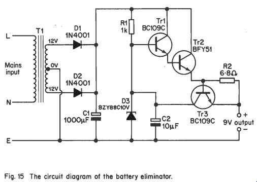
Fig. 15
The stabilizer circuit is a simple series type using RI, D3 and C2 to provide a stabilized potential having a nominal level of 10 volts. The zener current varies from about 8 mA under zero load conditions down to about 3 mA at full load. The dissipation in both R1 and D3 is therefore very low, and low power devices can be used in both positions.
A Darlington pair emitter follower is used as the output buffer amplifier, and the combined current gain of Tr1 and Tr2 is typically about 30,000 at maximum output, and has a minimum figure of about 10,000. With an input current of about 3 mA under full load conditions, and a minimum gain through the buffer amplifier of approximately 10,000, there is very little variation in the voltage drop through the amplifier with varying load currents. The actual voltage drop through the output amplifier is about 1.3 volts, and with a nominal 10 volt input this gives an output of approximately 8.7 volts. This is close enough to the required figure of 9 volts when one considers that the actual output voltage of a 9 volt battery varies from about 9.5 volts down to only about 7.5 volts during its lifespan.
Components Battery Eliminator (Figure 15)
Resistors. (Both are 1/3 watt 5%).
R1 1k
R2 6.8 ohms
Capacitors
C1 1000µF 25V
C2 10 uF 25V
Semiconductors
Tr1 BC109C
Tr2 BFY51
Tr3 BC109C
D1 1N4001
D2 1N4001
D3 BZY88C10V (10y, 400 mW zener diode)
Transformer
T1
Standard mains primary, 12-0-12 volt 100 mA secondary
Miscellaneous
Case, output connector, mains lead, circuit board, wire, solder etc.
Current Limiting
In this type of circuit it is normal to incorporate some form of output short circuit protection. The reason this is necessary is that in order to give good regulation the unit must have a very low output impedance. Because of this very low source impedance a very high output current will flow if the output of the unit is accidentally short circuited. This could easily result in the output transistor, and possibly some of the other components, being almost instantly destroyed. An ordinary fuse is not likely to provide adequate protection as the damage would almost certainly be done before the fuse blew and cut off the supply.
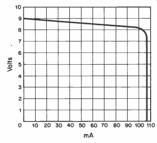
Fig. 16 Graph showing the effect of the current limiting circuit.
The most common form of short circuit protection, and the one used here, is current limiting. This consists of additional circuitry which has no significant effect under normal operating conditions, but which causes the output voltage to rapidly decline if too low an impedance is placed across the output.
In fact the output voltage reduces so rapidly with increased loading, that even with a short circuit placed across the output the current supplied by the unit is little more than its designed maximum level. The effect of a current limiting circuit is shown in the graph of Figure 16 which shows output voltage and current for a steadily decreasing load impedance, as obtained from the prototype Battery Eliminator unit.
The current limiting circuitry uses just two components; R2 and Tr3. It is so rapid in operation that there is no real risk of a short circuit on the output causing any damage to the output transistor or other components. The current limiting functions in the following manner.
R2 is connected in series with the output, and the voltage developed across this component is therefore proportional to the output current. At currents of up to about 100 mA the voltage developed across R2 will not be sufficient to switch on Tr3, which is a silicon type and has a stand-off voltage of about 0.65 volts.
At output currents of more than about 100 mA, the voltage across R2 gives Tr3 a strong enough forward bias to bring it into conduction. It then diverts some of the input current for Tr1 to the negative supply rail via the load. This tends to reduce the output voltage slightly. Increasing the loading on the output causes the voltage across R2 to rise, and takes Tr3 harder into conduction. This results in more of the drive current for Tr1 being diverted to earth through Tr3 and the load, and there is a large reduction in the output voltage. Even if a short circuit is placed across the output, Tr3 will be biased hard into conduction, and the output voltage reduced to virtually zero, and the output current will not be much more than about 100 mA.
In this way the required current limiting is obtained. One drawback of this simple circuit is that R2 reduces the output impedance of the unit, and produces a drop of about 0.65 volts in the output voltage between minimum and maximum loading, as can be seen from Figure 16. In this particular application this is of no real importance because a 9 volt battery has an internal resistance of several ohms, and so the regulation of the Battery Eliminator is probably still better than that of an ordinary 9 volt battery, even a large type such as a PP9.
In applications where the loss of regulation efficiency produced by the current limiting circuitry would be unacceptable, the current limit sense resistor must be added at the input of the regulator circuitry, and not at the output. One method of achieving this is shown in Figure 17.
Input Current limit transistor
Output Current sense resistor
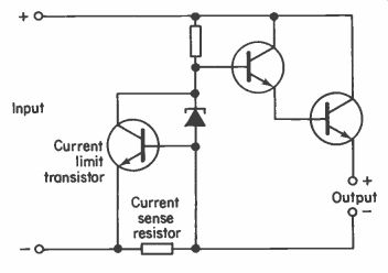
Fig.17 The current limiting circuit can be added ahead of the regulator to
give improved stabilization.
High Performance Regulators
Another method of overcoming this problem is to use a more complicated, but very high performance regulator, where the circuit compares the output voltage to a highly stable reference voltage, and maintains the two at precisely the same level by means of a feedback action. This type of circuit automatically compensates for changes in the output voltage due to losses in the current limiting circuitry, and, in fact, compensates for all changes in the output voltage, whatever the cause.
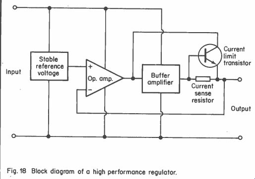
Fig.18
Figure 18 shows in block diagram form the basic arrangement of this type of regulator. The non-inverting (+) input of an operational amplifier is fed from a highly stable reference voltage source. This could be a simple zener stabilizer, a zener diode fed from a constant current source so as to give improved results, or some other form of improved reference source.
The output of the operational amplifier is taken to the output of the supply via a buffer amplifier which gives a high output current capability, and a current limiting circuit of the type described earlier. Negative feedback is applied from the output of the supply to the inverting (-) input of the operational amplifier.
An operational amplifier has an extremely high voltage gain, the gain of most devices being typically about 100,000 or 200,000 times! What the device is actually amplifying is the voltage. difference across the two inputs. If the inverting input is the one which is at the higher potential, the output goes negative. If it is the non-inverting input that is at the higher voltage, the output goes positive.
Due to the negative feedback from the output to the inverting input, the output is stabilized at the reference voltage. As the reference voltage is highly stable, so is the output voltage as well.
The stabilization process functions in the following manner.
If the output should be at a higher potential than the reference source, the inverting input of the operational amplifier will obviously be at a higher voltage than the non-inverting input.
This causes the output to go negative to a point where the two input voltages are balanced, remembering that the operational amplifier has a very high level of voltage gain, and a minute voltage across the inputs is enough to produce a considerable change in the output voltage. If the output voltage should drop below the reference voltage, this again produces a voltage difference across the inputs, this time of the opposite polarity, causing the output to swing positive. It can only swing sufficiently positive to balance the inputs, because as we have already seen, if it should go excessively positive, the inputs will be unbalanced and the output will be sent negative to correct the error. In this type of circuit the operational amplifier is sometimes referred to as an 'error amplifier', since it does in fact amplify any error in the output voltage. But more than this, its output is used to correct the error.
In simple discrete circuits of this type the operational amplifier is often a very simple circuit which has only a fairly low voltage gain. While this does not give a level of performance equal to that which can be obtained using a proper high gain amplifier, in practice it still gives perfectly adequate results with the output normally being stabilized to within 100 mV or so of its nominal level, and sometimes considerably better than this.
Note that because the feedback to the inverting input is taken from output of the supply and not from the output of the buffer amplifier, the stabilization action compensates for variations in output voltage due to changes in the voltage dropped across the current sense resistor.
Three-Terminal Regulators
It is becoming increasingly uncommon to find discrete voltage regulators of the type described above in new designs. High performance monolithic voltage regulators are available at quite low prices these days, and it is usually much less expensive and easier to use one of these, than to produce a discrete equivalent.
These i.c.s are extremely simple to use, as can be seen from the circuit diagram of Figure 19 which shows the basic way in which these devices are employed. The three terminals are, for obvious reasons, called the input, common and output. The input voltage is simply taken to the input and common terminals, and the stabilized voltage is available across the output and common terminals. The only discrete components required are a capacitor across the input and another across the output.
These are both needed to aid the stability of the regulator, and the one at the output also helps to give the supply a good transient response. The values of these capacitors are not critical, and are usually 100 nf, 220 nf or 330 nf.
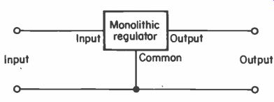
Fig. 19 Method using a three terminal regulator.
Types Available The most popular types of fixed voltage monolithic voltage regulators are the 78 ... series positive regulators, and the 79 series negative regulators. These are available in three output current ratings. This gives nine positive types and nine negative types, as shown in the table provided below.
Positive Types
Voltage 100 mA max. 500 mA max. 1A max.
5 78L05 78M05 7805
12 78L12 78M12 7812 15 78L15 78M15 7815
Negative Types
5 79L05 79M05 7905 12 79L12 79M12 7912 15 79L15 79M15 7915
Most supplies have additional voltages in both positive and negative types, typical voltages for these being 8, 9, 10, 18 and 24 volts. Some devices have suffix letters or numbers, depending on the particular manufacturer concerned, but they are all basically the same. Many component retailers do not actually sell these regulators by type number, but simply state the polarity, voltage and current ratings, and possibly the type of encapsulation the device has. There is actually a very wide range of these devices available, and it is possible to find a suitable type for most applications.
These devices have current limiting output short circuit protection, and in medium and high power types this is normally of the foldback type. Foldback current limiting is where an overload on the output is not merely counteracted by the output current being limited to a safe level, but by the output current actually reducing! The response of a foldback current limiting circuit is shown in Figure 20, which clearly shows how the output current reduces under overload conditions to typically less than half the maximum output current.
The main reason for using foldback current limiting is that it substantially reduces the dissipation in the regulator under short circuit conditions. For example, if a regulator has an input voltage of 10 volts under full load, and provides an output current of up to 1 amp. and an output of 5 volts, under full load there is 5 volts dropped across the regulator and it passes 1 amp. This obviously gives a maximum dissipation of 5 watts.
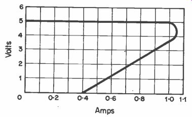
Fig. 20 The output voltage/current of a regulator having foldback current
limiting.
Under short circuit conditions there will still be an output current of 1 amp. or thereabouts if straightforward current limiting is used, and the input voltage will still be 10 volts.
However, this full 10 volts would be developed across the regulator, giving a dissipation of 10 watts, exactly double the normal working maximum dissipation in the device.
With foldback current limiting the full 10 volt supply would still be developed across the regulator, but the short circuit current might be, say 400 mA, giving a dissipation in the device of only 4 watts. This is less than the maximum power developed in the regulator under normal working conditions, and there is no danger of the device burning out.
Most monolithic voltage regulators also have thermal shutdown protection circuitry which reduces the output current if the device should start to overheat. These i.c.s. are therefore very hardy, and not easily destroyed by misuse.
One way they can be damaged is by an excessive input voltage.
There are differences in the maximum permissible input voltages quoted by various manufacturers for devices of the same basic type, but 25 volts seems to be the lowest quoted for any 5 volt device. Higher voltage devices are capable of withstanding at least 30 volts, and for 20 and 24 volt types the figure is 40 volts.
For the circuit to function properly the input voltage must not drop below 2.5 volts more than the output voltage, except for 5 volt types where it must not be less than 2 volts above the output potential.
The quiescent current of these i.c.s. is between about 1 and 5 mA, apart from a few very high power types which have a quiescent current of 10 mA. The line regulation for most types is less than 1% (i.e. varying the input voltage from the minimum to the maximum acceptable level causes a change in the output voltage of less than 1%). The load regulation is also typically less than 1% for most of these i.c.s. (i.e. varying the output current from zero to maximum causes a change in the output potential of less than 1%). The majority of devices have a ripple rejection figure of about 60 dB, and an output noise level of less than 100 microvolts.
When using these devices it is important to keep in mind that they can only handle a limited power dissipation, and the input voltage under full load should not be more than a few volts higher than the output voltage. The maximum power rating in free air of the low, medium, and high power types is 0.7 watts, 1 watt and, and 2 watts respectively. These are raised to 1.7 watts, 5 watts and 15 watts respectively with the device mounted on an infinite heat sink (which cannot, of course, be quite achieved in practice). The power dissipated in the device is equal to the difference between the input and output voltages, multiplied by the output current.
15V 800 mA
Supply
As an example of a power supply design using a fixed voltage monolithic voltage regulator, we will assume that we require a supply to deliver (say) +15 volts at up to 800 mA. This can be provided using the circuit shown in Figure 21.
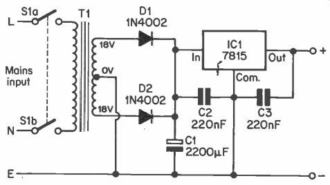
Fig. 21 A supply capable of delivering +15 volts at 800mA.
At the input there is on/off switch S1 and step-down transformer T1. The latter is an 18-0-18 volt type with a secondary current rating of 1 amp. It feeds a push-pull full wave rectifier and an unloaded voltage of about 27 volts is produced across smoothing capacitor C1. A higher voltage transformer, such as a 20-0-20 volt type, is not really suitable as the unloaded d.c. voltage produced would be about 30 volts, and could easily be a little more. This is equal to or above the maximum input voltage that most 7815 i.c.s can take, and is therefore unacceptable. Some types do actually have a maximum input voltage rating of 35 volts, and could be used with a 20 volt transformer perfectly safely, provided that the constructor is sure that the device be or she is using is a 35 volt type. However, this would give increased power dissipation in the regulator.
A 15 volt type would not be suitable unless it had a fairly high current rating of about 2 amps or so, as the loaded supply voltage at the input of the regulator would otherwise be less than the minimum of 17.5 volts required by the regulator for proper operation.
C2 and C3 are the input and output decoupling capacitors for regulator device IC1, and these two capacitors should be mounted physically close to the regulator i.c. The 7815 is the obvious choice for IC1 since it is the smallest 15 volt positive regulator capable of handling the required maximum current of 800 mA.
Under full load there will be an input voltage to IC1 of something in the region of 19 to 20 volts, giving as much as 5 volts across the regulator. With a current of 800 mA this gives a dissipation of as much as 4 watts (0.8A x 5V = 4W). This is double the maximum of 2 watts that the 7815 can handle, and so the additional 2 watts must be 'dumped' into a heatsink.
A wide range of commercially made heatsinks are produced, and these are given a rating of so many degrees per watt. This is simply the rise in temperature that occurs for each watt of energy transferred into the heatsink, and the larger the heatsink, the lower the number of degrees per watt. The minimum amount of heatsinking required is calculated in the following way.
We must first know the maximum air temperature in which the equipment is to be used, and unless the equipment is going to be used in an unusually hot environment 30 degrees Celsius is a safe assumption. It is then necessary to know the maximum safe temperature for the i.c., and for monolithic regulators this is 125 degrees Celsius. However, this is the junction temperature, and not the case temperature that can be tolerated. The maximum acceptable case temperature is about 100 degrees Celsius. This means that the device must not be allowed to rise by more than 70 degrees Celsius (from 30 degrees to 100 degrees = 70 degrees).
As a power of 2 watts must cause an increase in temperature of no more than 70 degrees, a heatsink having a rating of 35 degrees Celsius per watt or less (70 degrees divided by 2 watts = 35 degrees C. per watt) is required. In practice a somewhat larger heatsink is needed, as even using silicon grease or a substitute between the i.c. and the heatsink, there will be less than a 100% transfer of heat from one to the other. Also, in the interests of good long term reliability is not advisable to have the i.c. operating just below its maximum safe temperature. If possible it should work below this level with a safety margin of 20 degrees or more. A small bolt-on heatsink having a rating of about 17 degrees Celsius per watt is therefore the smallest heatsink that is likely to be satisfactory in practice, and a larger type should be used if possible.
If the regulator i.c. is mounted inside an enclosed case where it will not be in free air, but a pocket of trapped air that will be heated by the regulator and probably by other components inside the case as well, an even larger heatsink would be needed.
How much larger depends upon the individual circumstances, but it would typically need to be two or even three times as large.
If the equipment is to be housed in a metal case, or a case having a metal chassis, the case or chassis can usually be used to provide adequate heatsinking. It is not normally necessary to insulate the regulator from the heatsink, case, or chassis, as the heat-tab of the regulator connects to the common terminal internally, and so the heatsink, case, chassis, and heat-tab will normally all be at the same potential.
Note that if a negative output version of the supply is required, it is merely necessary to reverse the polarity of D1, D2 and C1, and to replace IC1 with a 7915 device.
Components # 15 Volt, 800 mA. Supply (Figure 21)
Capacitors
C1 2200 µF 40V C2 220 nF plastic foil C3 220 nF plastic foil
Semiconductors IC1 7815 (15 volt, 1 amp. positive regulator)
D1 1N4002
D2 1N4002
Transformer
T1 Standard mains primary, 18-0-18V, 1 amp secondary.
Switch S1 D.P.S.T. rotary mains or toggle switch
Miscellaneous
Case, output sockets, circuit board, mains lead, wire, solder etc.
Dual Supply
Because fixed voltage monolithic regulators are available in both negative and positive versions, they are ideal for use where dual balanced supplies are required. If, for example, a supply is required for an operational amplifier-based circuit requiring positive and negative supplies of 12 volts at 100 mA, the circuit of Figure 22 could be used.
Here T1 is a 15-0-15 volt transformer having a secondary current rating of 200 mA or more. There are two push-pull full wave rectifiers; D2 and D3 which provide a positive output, and D1 plus D4 which provide a negative output. The positive supply is smoothed by C1 and the negative one is smoothed by C2. IC1 provides regulation of the positive supply, and IC2 acts as the negative supply regulator. C3 to C6 are the decoupling capacitors for, the regulators, and should be mounted physically close to their respective devices in order to ensure good stability.
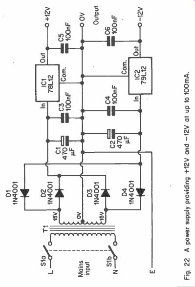
Figure 22
The power developed across each regulator will be several hundred milliwatts, and both devices will operate quite hot if the maximum 100 mA (or virtually the full 100 mA) is drawn from the unit continuously. However, it is unlikely that any heatsinking will be needed.
Components ± 12 Volt, 100 mA. Supply (Figure 22)
Capacitors C1, C2 470 uF 25V (2 off)
C3 to C6 100 nF plastic foil (4 off)
Semiconductors
IC1 78L12 (12 volt, 100 mA. positive regulator)
IC2 79L12 (12 volt, 100 mA. negative regulator)
D1 to D4 1N4001 (4 off)
Transformer
T1 Standard mains primary, 15-0-15 volt 200 mA (or more) secondary
Switch S1 D.P.S.T. rotary mains or toggle switch
Miscellaneous
Case, output sockets, circuit board, mains lead, wire, solder etc.
Higher Output Voltage
The method shown in Figure 22 can also be used when the required output voltage is higher than can be obtained using a single regulator. For example, two 15 volt regulators used in this arrangement will provide 30 volts, and two 24 volt types give 48 volts. The OV output is ignored, and the output is taken from across the positive and negative outputs only. The appropriate connection should be connected to the mains earth lead.
Increased Output Voltage
Although there is an increasingly large range of voltages available these days, there is by no means a regulator to suit every requirement. It is possible to obtain a small increase in the output voltage from a voltage regulator by using a few additional components, and this method helps to fill in some of the voltages for which no regulator is available. This basic method of obtaining this increased output voltage is shown in Figure 23.
Here it has been assumed that the desired output voltage is approximately 6V. This can be obtained using a 5 volt regulator in a circuit designed to boost the output by 1 volt, and this is achieved by merely adding two silicon rectifiers in the common lead of the regulator, as shown in the diagram.
The rectifiers are connected so that they are forward biased by the quiescent current which is drawn by the regulator, and which flows through the common terminal. The rectifiers therefore act rather like low voltage zener diodes, each having a zener voltage of about 0.5 to 0.6 volts, and giving a combined zener voltage of about 1 to 1.2 volts.
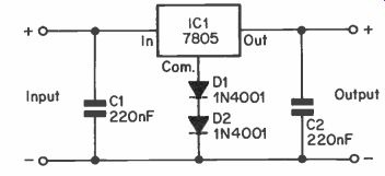
Fig. 23 Method of increasing the output voltage of a three terminal regulator.
Their effect is to raise the common terminal of the regulator to 1 volt or so above the earth rail potential. The regulator actually stabilizes the output at 5 volts above the common terminal's potential, and not 5 volts above the earth rail.
Therefore, by raising the common terminal by 1 volt or so, the output is raised by the same amount, bringing it to the required level of 6 volts or marginally more.
This method can be used with any three terminal regulator, although with some small types the author has come across, it has been necessary to add a resistor of a few kilohms in value between the output and common terminals in order to obtain satisfactory operation. The amount by which the output is raised can be altered by varying the number of rectifiers used.
Ordinary small silicon diodes such as the 1N41 48 can also be used, but the output is then raised by about 0.6 to 0.7 volts per diode. It is also possible to use a zener diode or amplified diode to raise the potential at the common terminal, but it is not advisable to attempt to obtain a rise in the output potential of more than a few volts. This arrangement also works with the 79 .. series of negative voltage regulators, provided the diode(s) or transistor is connected with the correct polarity.
The current limiting and thermal protection circuits of the regulators still function satisfactorily when the method described here is used.
Components (Figure 23)
Semiconductors
IC1 7805 (5 volt, 1 amp regulator)
D1, D2 1N4001 (2 off)
Capacitors C1, C2 220 nF plastic foil (2 off)
Increased Current
It is possible to obtain increased output current from a monolithic voltage regulator, and one method of doing so is shown in the circuit diagram of Figure 24. The ratio of R1 to R2 ensures that for each milliamp of current that flows in R1, D1 and the regulator, a little over 4 mA is directed through Tr1 and R2. Thus with the full 1 amp passing through IC1, there is a current of over 4 amps flowing through Tr1, and the circuit provides a maximum output current of slightly in excess of 5 amps.
Even in the event of an overload, the currents through Tr1 and IC1 still have a ratio of slightly more than 4 to 1, and so the current limiting is still effective.
Circuits of this type are becoming unnecessary these days due to the arrival of very high power regulators such as the 78H05, 781-112 etc., which have a maximum current rating of 5 amps, and are used in precisely the same way as the other three terminal monolithic regulators.
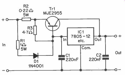
Fig. 24 A method of obtaining increased output current.
Components (Figure 24)
Resistors
R1 1 ohm 5 watt 5%
R2 0.22 ohms 5 watt 5%
R3 4.7 ohms 1/2 watt 10%
Capacitors C1, C2 220 nF plastic foil (2 off)
Semiconductors
Tr1 MJE2955
D1 1N4001
IC1 1 amp positive regulator