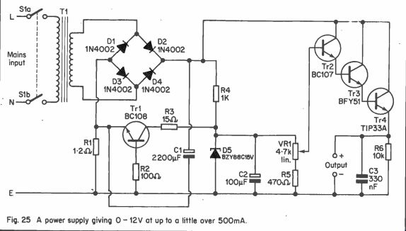
Fig. 25 A power supply giving 0-12V at up to a little over 500mA.
| Home | Audio mag. | Stereo Review mag. | High Fidelity mag. | AE/AA mag. |
Variable voltage stabilized supplies are basically the same as fixed voltage types, but have a potentiometer added into the circuit at the appropriate point. Circuits of this type are primarily used as bench and workshop power supplies, but they can also be used where an item of equipment requires a supply voltage that would be difficult to produce using a fixed voltage circuit. In this case the potentiometer is a preset type which is used to trim the output voltage of the supply to the desired level.
Simple Bench Supply
The circuit of Figure 25 is for a simple bench power supply is continuously variable from zero to slightly more than 12 volts. A maximum current of over 500 mA is available, and the noise and ripple on the output are no more than about 1 mV at any output current and voltage within the working range of the unit. The maximum variation in the output voltage between minimum and maximum loading is only about 300 mV. The unit is suitable for testing and developing most electronic projects, although it does not have sufficient output for high power equipment, such as audio power amplifiers having an output of more than a few watts.
T1 is a transformer having a secondary rated at 18 volts and 1 amp, or a 9-0-9 volt type can be used if the center tap is ignored. A 17 volt 1 amp battery charger transformer is also suitable. Its output is full wave rectified by the bridge rectifier formed by D1 to D4, and the output from the rectifier is well smoothed by C1.
Fig. 25 A power supply giving 0-12V at up to a little over 500mA.
The regulator is basically the same as that shown in Figure 13(b), and described in the previous section. The only difference is that a potential divider circuit has been added between the output of the zener stabilizer, and the input to the buffer amplifier. This potential divider is formed by VR1 and R5, and the output at VR1's slider can be varied from only about 1.4 volts when it is at the bottom of its track, up to the nominal 15 volt zener voltage when it is at the top of its track.
There is approximately 2 volts dropped through the output buffer stage, giving an output voltage range from zero up to typically 13 volts. However, the upper limit is subject to component tolerances, such as the 5% tolerance on the zener voltage, and so the maximum output potential is only guaranteed to be a little in excess of 12 volts, Some form of effective overload protection circuit is really essential in a bench power supply, where frequent accidental overloads and short circuits are likely to occur. In this circuit simple current limiting is used, and is provided by Tr1 and its associated components.
Under normal operating conditions the voltage developed across R1, which is connected in series with the output of the supply., is insufficient to bias Tr1 into conduction. The circuit is then allowed to function normally, apart from a small and insignificant voltage drop across Rl. This does not adversely effect the regulation efficiency of the unit since it has been added ahead of the regulator circuitry.
If an overload occult, the voltage across R1 will rise to about 0.65 volts, and Tr1 will be switched on by the base current it receives via current limiting resistor R2. A fairly strong current is then drawn through Tr1 and current limiting resistor R3, causing an increased voltage drop across R4, and the output voltage to be reduced. This limits the output current to no more than about 550 to 600 mA even with a short circuit on the output, as the current limit circuitry then reduces the output voltage to virtually zero.
R6 is a load resistor and merely ensures that the output current never becomes so low that the buffer amplifier fails to operate properly, producing the wrong output voltage. C3 helps to give the unit a good transient response.
The power dissipated in Tr4 depends upon the output voltage and current, and is at a maximum with low output voltages and high output currents (or the output short circuited, which gives the same effect). Under worst case conditions there is likely to be about 20 volts across Tr4, and it will be passing a current of about 600 mA. This gives a power dissipation in the device of around 12 watts. In order to withstand this indefinitely it should be mounted on a substantial heatsink. A type having a rating of about 3 degrees Celsius per watt should be satisfactory even if the device is mounted inside an unventilated case. A smaller type having a rating of about 4.5 degrees Celsius per watt should be suitable if the device is mounted in free air.
VR1 can be fitted with a large control knob having a scale calibrated in terms of output voltage. A multimeter can be used when calibrating this. Alternatively a voltmeter can be added across the output, but the problem here is that it is unlikely that a meter having an ideal full scale value will be obtainable. Voltmeters having fairly high full scale values are readily available; but would not give an acceptable level of accuracy at the relatively low voltages involved here. It may be possible to obtain a 0 to 15 volt type, and this would be perfectly suitable. The alternative is to use a current meter with a suitable series resistor to give the required full scale value.
The value of the required resistor is given by dividing the required full scale voltage by the full scale current reading of the meter. Thus in order to obtain a full scale value of (say) 15 volts with a 100 µA f.s.d. meter, the resistor must have a value of 15 volts divided by 0.0001 amps (100 µA) which equals 150,000 ohms, or 150k in other words. Actually this gives the required total resistance for the meter and the series resistor, and so the coil resistance of the meter should be subtracted from the answer. However, in practice, when a f.s.d. value of several volts or more is required, the resistance of the meter will be so low in comparison with the series resistor that it can be ignored. If the calculated resistance does not coincide with a preferred value, the nearest preferred value can be selected provided it is within about 1% of the calculated value. If not, then two or more resistors connected in series must be used to make up the required value. The series resistor or resistors should have a close tolerance of 2% or better. The meter should obviously not have a very high f.s.d. value, or it would heavily load the power supply. A f.s.d. value of about 1 mA or less is suitable.
An alternative method is to use a preset resistor in series with the meter, and this can be used to set the voltmeter sensitivity at the correct level using a multimeter as a calibration standard.
The value of the preset can be calculated using the method described above, and then adding 50 to 100% to the answer.
A preferred value in which presets are available should fall within this range, or close to one of the limits.
One problem with using a current meter plus series resistor as a voltmeter is that it will almost certainly be necessary to recalibrate the meter. Most modern meters have a plastic front section which simply clips on and off. With this removed, the unwanted scale markings can usually be carefully scratched off with the point of a compass, or if this tends to remove both the markings and the white overall covering of the scale plate, it might be better to paint out the markings using white enamel paint. Various forms of rub-on and stick-on lettering and numbering are available, and it is not too difficult to recalibrate a meter scale using these.
If recalibration of a meter is undertaken, it should be borne in mind that a meter movement is very delicate, and is easily damaged. Great care must therefore be taken to avoid damaging the meter movement once the front cover of the meter has been removed. The scale plate of every meter the author has come across is easily removed from the rest of the meter, and it is normally just a matter of removing two small screws.
Recalibration will probably be much easier if this is done, and the risk of the meter becoming damaged will almost certainly be considerably reduced.
Components 0-12 Volt, 500 mA.
Supply (Figure 25)
Resistors. (All 1/3 watt 5%).
R1 1.2 ohms
R2 100 ohms
R3 15 ohms
R4 1k
R5 470 ohms
R6 10k
VR1 4.7k lin. Carbon
Capacitors
C1 2200µF 40V
C2 1001ff 25V C3 330 nF plastic foil
Semiconductors
Tr1 BC108 Tr2 BC107 Tr3 BFY51 Tr4 TIP33A D1 to D4 1N4002 (4 off) D5 BZY88C15V (15 volt, 400 mW zener)
Transformer
T1
Standard mains primary, 17 or 18 volt, 1 amp secondary
Switch S1 D.P.S.T. rotary mains or toggle type
Miscellaneous
Case, output sockets, circuit board, mains lead, wire, solder etc.
Current Meter
An output current meter is a very useful feature to have on a workshop power supply, and it can quickly show up an excessive current consumption by the supplied equipment, enabling remedial action to be taken before serious damage occurs to the supplied equipment.
While it is possible to simply add a current meter of a suitable full scale value in series with the output, this does have the disadvantage of reducing the output impedance of the supply.
and degrading the regulation efficiency. It would be preferable to add the meter ahead of the regulator circuit. For example, an output current meter could be added to the circuit of Figure 25 between the junction of D2, D4, C1 and R4, and the junction of Tr2 to Tr4 collectors. The meter would then read fractionally high as it would register the small quiescent output current as well as the current drawn by the load. This is of no real practical consequence though, as the quiescent current drawn by the output buffer amplifier is so low in comparison to the full scale value of the meter (which could be 500 mA or 1A in this example).
An alternative method of adding an output current meter to the unit is shown in Figure 26. Here the current sense resistor of the current limiting circuit ( R1) is used as the shunt resistor for a sensitive current meter, and reduces its sensitivity to the correct level. The resistance through the meter circuit is very high when compared to the resistance of R1, and so the addition of the meter circuit does not have any significant effect on the current limiting circuitry.
R1 is connected in series with the output, and the voltage developed across this resistance is therefore proportional to the output current (if we ignore the small and insignificant Fig. 26 A method of adding an output current meter to the circuit of Fig. 25. current drawn by the regulator circuitry). MEI and R7 effectively form a voltmeter circuit which registers the voltage developed across R1, and R7 is adjusted to give a full scale sensitivity of 0.6V. From Ohms Law it is apparent that in order to give 0.6V across R1 , an output current of 500 mA (0.5A) is required (I = E/R, I = 0.6 ÷ 1.2, = 0.5A). The meter thus effectively reads 0 to 500 mA., and does not need any recalibration as it already has a 0 to 500 scale.
There is no need to include any meter overload protection circuitry when including an output current meter in a power supply which has current limiting overload protection, since the current limiting prevents any serious overloading of the meter from occurring.
Components Optional Meter Circuit
( Figure 26) R7 2.2k 0.25W preset MEI 500 µA. moving coil panel meter The 723C I.C.
The 723C integrated circuit is a 'standard' i.c. voltage regulator which has been designed to be capable of fulfilling most voltage regulator applications. It can be used as a positive regulator, negative regulator, and as a switching regulator (a highly efficient type of circuit where the output buffer stage is switched on and off at high speed, and dissipates very little power). It can be connected to give straightforward current limiting or foldback current limiting. There is far too little space available here to describe this device in detail, together with the various ways of utilizing it, but the more important aspects of the device will be considered.
The output voltage range of the device is 2 volts minimum up to 37 volts maximum. The maximum permissible output current is 150 mA., but in practice the output current will often need to be limited to considerably less than this figure to keep within the maximum permissible dissipation for the device, which is 500 mW. The maximum input voltage should be no more than 50 volts peak, and 40 volts continuous. The minimum input voltage is 9.5 volts, or 3 volts more than the maximum output voltage required, whichever is the greater.
The maximum permissible input output voltage differential is 37 volts.
Figure 27 shows in block diagram form the basic arrangement of the 723C's internal circuitry. It consists of a highly stable reference voltage having a nominal potential of 7 volts, an operational amplifier, a buffer amplifier, and a current limiting transistor. It is really a regulator of the type previously outlined in the block diagram of Figure 18, and described in the previous section. However, instead of the inverting input of the operational amplifier being connected to the output of the circuit, it is brought out to a pin of the device. It is normally taken to the wiper contact of an external potentiometer connected across the output of the circuit. If the wiper of this potentiometer is taken to the top of its track, the circuit operates in exactly the same manner as the fixed voltage type outlined in Figure 18 and described in the previous section, with the output being stabilized at the same potential as the reference voltage.
If the slider of the potentiometer is brought down its track, rather than stabilizing the output at the same potential as the reference voltage, the circuit stabilizes the inverting input of the operational amplifier at this potential. Due to the voltage drop across the potentiometer, the output must rise to a higher potential in order to bring the inverting input to the appropriate voltage. The further down its track the slider is taken, the greater the voltage drop through the potentiometer, and the higher the output voltage becomes. If, for instance, the slider is taken two thirds of the way down its track, the voltage fed to the inverting input of the operational amplifier will only be one third of the output voltage. The output is thus stabilized at three times the reference voltage so that the appropriate voltage is maintained at the inverting input of the operational amplifier. Thus a variable output voltage is obtained, together with a very efficient stabilizing action.
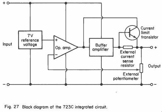
Fig. 27.
The current sense resistor of the current limiting circuit is made of a discrete component so that the maximum output current can be varied to suit individual requirements.
The output voltage of the 723C is approximately equal to 7 (R1 + R2)/R2 volts, where R1 is the resistance between the output and the inverting input of the operational amplifier, and R2 is the resistance between the inverting input and the negative supply rail. This assumes that the reference voltage is coupled direct to the non-inverting input of the operational amplifier, or these two points are coupled via a fairly low value resistor. It is not essential to do this, and the reference voltage can be fed to the non-inverting input via a potential divider, so that the reference voltage supplied to the operational amplifier is less than 7 volts. In fact it is essential to do this if an output voltage of less than 7 volts is required, since the output voltage cannot be less (under normal working conditions) than the reference voltage at the non-inverting input of the operational amplifier. The lowest reference voltage that can be successfully employed in a 723C based circuit is 2 volts. If a reference voltage of less than 7 volts is used, then the 7 in the above equation must be replaced by whatever reference voltage is used.
The value of the current limiting sense resistor is equal to 0.66 divided by the required maximum output current.
3.5 to 20V 1.5A Supply
Figure 28 shows a practical example of a circuit using the 723C integrated circuit, and this is for a bench power supply having an output voltage range of 3.5 to 20 volts nominal, and capable of providing a maximum output current of 1.5 amps.
Three switched levels of current limiting are available at 15 mA., 150 mA., and 1.5A. (approximately).
The mains supply is taken to the primary winding of step down transformer T1 by way of on/off switch Si. LP1 is an on/off indicator lamp, and this is a neon type having an integral series resistor for 240V mains operation. The output from the secondary of T1, which has a rating of 20 volts at 2 amps or more, is full wave rectified by D1 to D4, and smoothed by C1.
In order to provide the minimum output voltage of 3.5 volts it is necessary to couple the output of the reference source at pin 6 of IC1 to the non-inverting input of the operational amplifier at pin 6 via a suitable potential divider. The potential divider is formed by R1 and R2, and as the two resistors have the same value, the 7 volt input is halved to give an output of 3.5 volts.
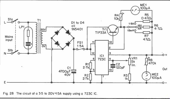
Fig. 28 The circuit of a 3.5 to 20V-1.54 supply using a 723C IC.
The positive output of the unregulated supply is connected to the positive supply terminal of IC1 (pin 12) and the positive input of the buffer amplifier in IC1 (pin 11) via fuse FS1.
As the current and power handling capabilities of the 723C are inadequate for this application, the output terminal of the device (pin 10) is used to drive an emitter follower buffer stage using discrete transistor Tr1. This feeds the output from its emitter terminal via whichever of the three current limit sense resistors is selected using S2. These three resistors provide the three limit currents. MEI is an output current meter, and this is of basically the same type as the one shown in Figure 26 and described earlier. R4 is adjusted to give a full scale value of 20 mA., 200 mA., and 2A. (the full scale value changes according to the current limit level selected). This is much better than having a straightforward 0 to 2A. current meter which would give no significant deflection at output currents of up to about 100 mA. or so, and would therefore be of comparatively little value. On the 15 mA. current limit range, where the meter reads 0 to 20 mA., there will be a small deflection of the meter under quiescent conditions due to the current drawn by VR1 and R3. This is unavoidable, but fortunately it is not really very troublesome in practice.
VR1 and R3 set the voltage range of the unit, and this is continuously variable from about 3.5 volts with VR1's slider at the top of its track, up to about 23 volts with the slider at the bottom of its track. The upper limit is purposely made rather more than the required limit of 20 volts so that even if the actual maximum output voltage is somewhat less than the theoretical value, due to component tolerances, the required figure of 20 volts should still be attainable. The lower limit of 3.5 volts is also a nominal one, and will vary somewhat from one unit to another. In order to minimize errors in the output voltage range it is advisable to make R1, R2 and R3 all 1 or 2% types.
C2 is the compensation capacitor for the operational amplifier contained within the 723C, and it aids good stability. R8 and ME2 form an output voltage meter circuit, and R8 is adjusted for a full scale sensitivity of 25 volts. With most 100 microamp meters this gives a convenient one scale division per volt.
Tr1 has to dissipate a power of around 30 watts at minimum output voltage and maximum output current, and it is therefore advisable to mount it on a large heatsink rated at about 2.5 degrees Celsius per watt, and mounted on the exterior of the case. R5 has to dissipate about 1 watt under full output current conditions, and so it would be advisable to give this a conservative rating of 2 watts or more. In order to give good consistency between the three current meter ranges, R5 to R7 should have a tolerance of 5% or better.
Components 3.5-20 Volt, 1.5A Supply (Figure 28)
Resistors R1 2.7k 1/3 watt 2% or better R2 2.7k 1/3 watt 2% or better R3 1k 1/3 watt 2% or better R4 10k 0.25 watt preset R5 0.47 ohms 2 watt 5% R6 4.7 ohms 1/3 watt 5% R7 47 ohms 1/3 watt 5% R8 470k 0.25 watt preset VR1 4.7k or 5k lin. carbon Capacitors C1 4700 AF 40V C2 120 pF ceramic plate
Semiconductors
IC1 723C (14 pin DIL) Tr1 TIP33A D1 to D4 1N5401 (4 off)
Transformer T1 Standard mains primary, 20 volt 2 amp secondary
Switches S1 D.P.S.T. rotary mains or toggle type S2 3 way single pole rotary type capable of switching 1.5A
Fuse FS1 1.5A 20mm quick blow type
Lamp LP1
Panel indicator neon having integral series resistor for use on 240V mains
Meters MEI, ME2 100 µA. moving coil panel meters (2 off)
Miscellaneous
Case, output sockets, circuit board, mains lead, wire, 20mm chassis mounting fuseholder, solder etc.
Four Terminal Regulators
A four terminal voltage regulator is very similar to the three terminal type described in the previous section, but the inverting input of the internal operational amplifier is taken out to an additional terminal. This enables the output voltage to be readily varied by means of a potentiometer connected across the output, and feeding the additional (control) terminal of the device.
The basic method of using a four terminal monolithic voltage regulator is shown in Figure 29. This is very much the same as for a three terminal type, with decoupling capacitors across the output and input to aid good stability and transient response.
R1 and R2 form the potential divider which determines the Fig. 29 Basic method of using a four terminal regulator.
output voltage. The output voltage is equal to (R1 + R2)/R1 multiplied by the internal reference voltage of the device. Of course, in practice R1 and R2 would normally be replaced by a potentiometer so as to give a variable output, or by several switched preset potentiometers if several switched output voltages are required. A simple potential divider can be used though, where the output voltage required is one that is not easily obtained using a fixed voltage monolithic voltage regulator. There is no point in using a four-terminal regulator in an application where a three-terminal type could be used, because the four-terminal variety are substantially more expensive.
Four Voltage Supply
Figure 30 shows an example of a power supply using a four terminal monolithic voltage regulator. This is for a power supply having four switched output voltages of 6V, 7.5V, 9V and 12V, with a maximum output current of 500 mA. This can be used when designing or testing battery operated equipment such as transistor radios and portable cassette recorders.
It can also be used as a mains adaptor for equipment of this type which has a power socket (or if a power socket is added).
The circuit is very straightforward, and has the output from T1 full wave rectified by D1 and D2, and smoothed by C1. The regulator used is a p.A78MGU1C type, which has a 5 volt internal reference voltage, and can therefore give voltages down to 5 volts. The maximum output voltage for this device is 30 volts, and the maximum input voltage is 40 volts. For correct operation the input voltage should not be less than two volts above the required output voltage.
The output voltage is controlled by whichever of the four preset potentiometers (R1 to R4) is selected by S2, and these presets are simply adjusted to give the four output voltages stated earlier.
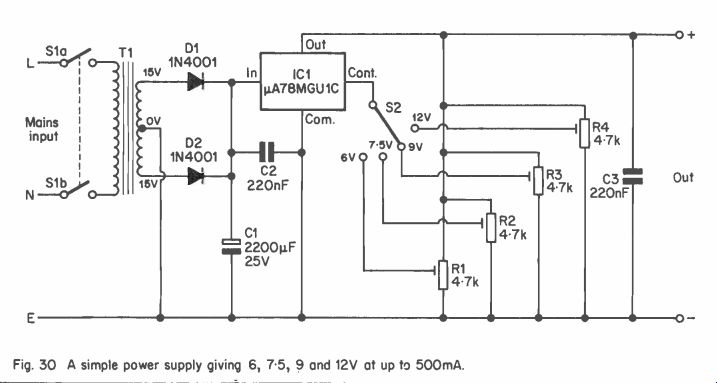
Fig. 30 A simple power supply giving 6, 7.5, 9 and 12V at up to 500mA.
T1 should have a secondary rating of 15-0-15 volts at 500 mA. or more. The maximum output current of the unit can be raised to 1 amp by using a mains transformer having a secondary current rating of 1 amp or more, and using a µA78GU1C device in the IC1 position. IC1, regardless of which type is used, should be mounted on a substantial heatsink as it has to dissipate several watts at certain combination of output current and voltage. Both the ttA78MGUI C and j.tA78GU1C devices have foldback current limiting and thermal protection circuitry.
Components Simple Power Supply (Figure 30) Resistors. (All 0.25 watt presets).
R1 to R4 4.7k (4 off)
Capacitors
C1 2200µF 25V C2, C3 220 nF plastic foil (2 off)
Semiconductors IC1 AA78MGU1C
D1, D2 1N4001 (2 off)
Transformer T1
Standard mains primary, 15-0-15 volt 500 mA.
secondary
Switches S1 D.P.S.T. rotary mains or toggle type S2 4 way 3 pole rotary (only one pole used)
Miscellaneous
Case, output sockets, circuit board, mains lead, wire, solder etc.
High Current Type
A high current four-terminal voltage regulator is available, and this is the I.tA78HGKC device which is capable of providing an output current of up to 5 amps. It has an output voltage range of 5 to 20 volts, and a maximum permissible input voltage of 25 volts. The input voltage should be at least 3.5 volts above the output voltage for proper operation of the device. It is a hybrid device which incorporates output current limiting and has thermal protection circuitry.
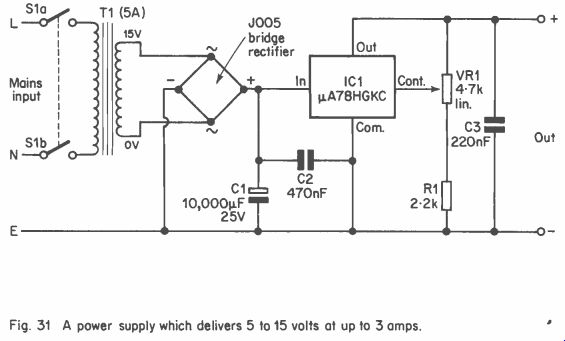
Figure 31
Figure 31 shows a simple circuit which employs this device, and this is for a bench power supply having an output voltage range of 5 to 15 volts (nominal) at a maximum current of 3 amps.
Negative versions of the four terminal voltage regulator devices mentioned here are available, and simply have a figure 9 in the type number instead of a figure 8 (./A79MGU1C etc.).
Components
5-15 Volts, 3 Amp Supply (Figure 31)
Resistors
R1 2.2k 1/3 watt 5%
VR1 4.7k lin. Carbon
Capacitors
C1 10,000 µF 25V
C2 470 nF plastic foil
C3 220 nF plastic foil
Semiconductors
IC1 µA78HGKC
Bridge rectifier J005
Transformer T1
Standard mains primary, 15 volt 5 amp secondary
Switch S1 D.P.S.T. rotary mains or toggle type
Miscellaneous
Case, output sockets, circuit board, mains lead, wire, solder etc.