SINCE VIDEO AND AUDIO signals cannot be propagated through space they must be carried by radio signals that can.
Adding audio or video information to a radio "carrier wave" is called modulation. In this section we shall discuss circuits used in amplitude modulation (AM), frequency modulation (FM) and phase modulation (PM), all of which are used in color television transmission. Pulse modulation, which is used in telemetry with spacecraft, will also be explained.
The modern radio and TV receiver is a superheterodyne receiver, in which the incoming modulated radio carrier is mixed with another radio-frequency signal generated in the receiver itself, and converted to an intermediate frequency (IF), which is then amplified in the IF amplifier (section 2). Since this is also modulation, we include mixers and converters in this section.
AMPLITUDE MODULATION
In AM we wish to vary the power of the transmitted signal in accordance with audio information, so we need a circuit in which the output of an RF amplifier is controlled by an audio signal. In such an amplifier the carrier signal generated in a previous stage is amplified by the addition of power by means of a vacuum tube or transistor.
The output-signal amplitude depends upon the type of circuit, tube characteristics and operating voltages. If one of the operating voltages is varied in accordance with an audio signal, the output power of the carrier will be varied proportionately.
PLATE MODULATION
In plate modulation, varying the plate voltage causes the DC current through the RF power amplifier tube to vary, thereby varying the output power. Figure 5.1 illustrates a typical circuit.
Distinguishing Features
The DC plate supply for the RF power amplifier comes through the secondary winding of a modulation transformer in the output circuit of an audio power amplifier. Both amplifiers may be single-ended or push-pull.
Uses
This circuit will be found in AM transmitters of all sizes.
Detailed Analysis
In Figure 5.1 the audio power amplifier is the same as those discussed in section 3, and its operation is identical. Similarly, the RF power amplifier is also the same as those described in the same section.
B+ current for the RF amplifier plate circuit has to pass through the secondary of T3. The audio signal from V3 and V4 is also present in the secondary of T3, and its variations in amplitude add to or sub tract from the DC supply voltage. The resulting variations in the plate supply voltage cause corresponding variations in the gain of V1 and V2, so that the output amplitude of the carrier fluctuates in accordance with the audio signal.
The degree to which the carrier is modulated depends upon the power of the audio signal, and is expressed as a percentage. In 100 percent modulation the carrier is driven all the way to zero at its minimum amplitude, and to double its "resting" amplitude at the maximum value. This requires that the audio power amplifier be capable of as great an output as the RF power amplifier. This might seem a draw back, but plate modulation is much more efficient than grid modulation because the RF power amplifier can be operated Class C (see Appendix).
GRID MODULATION
Figure 5.2 shows a grid modulation circuit.
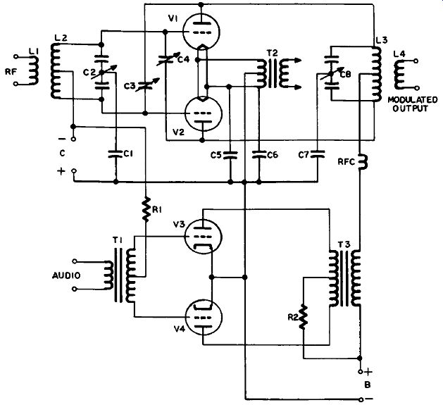
Figure 5.1 Plate Modulation
Distinguishing Features
The grid-bias supply voltage to the RF power amplifier is routed through the secondary winding of the modulation transformer in the audio power amplifier output. Both amplifiers may be single-ended or push-pull.
Detailed Analysis
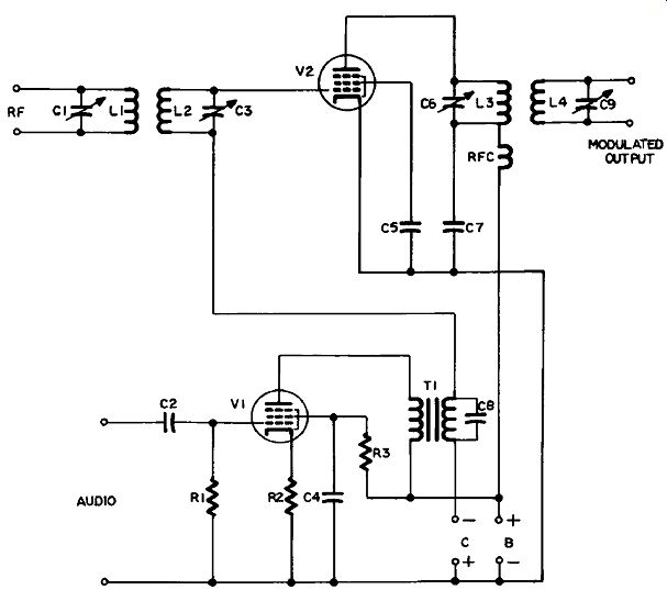
Figure 5.2 Grid Modulation
In Figure 5.2 both amplifiers are similar to those discussed in section 3, so will not be analyzed in detail here.
C- (grid bias voltage) for the RF amplifier is routed through the secondary winding of T1. The audio signal from V1 is also present in the secondary of T1, and its variations in amplitude add to or subtract from the DC supply. The resulting variations in the grid bias voltage cause corresponding variations in the gain of V2, so that the output amplitude of the carrier fluctuates in accordance with the audio signal.
The secondary of T1 is shunted by C8. This capacitor's value is such that while it does not bypass T1 for audio it does for RF. In this way a connection is provided from the lower end of L2 via C8 and the grid-bias power supply to the cathode of V2.
In grid modulation the audio power amplifier does not have to be as powerful as the RF amplifier it modulates, since the output power must all come from the RF amplifier. This amplifier can only be operated Class B, however, since the audio information would be lost in Class C operation. In Class B operation (see Appendix) the positive swings of the modulating signal are completely reproduced in the tube. The cut-off negative swings are restored by the "flywheel" action of the output tank circuit C6-L3, as explained in section 4.
FREQUENCY MODULATION
In FM we wish to vary the frequency of the transmitted signal in accordance with audio information, so we need a variable frequency oscillator in which the frequency of the signal generated is not fixed, but is controlled by an audio signal. The variable-frequency carrier may then be amplified in subsequent RF amplifier stages as necessary for broadcasting.
Varying the frequency of an oscillator can be achieved in various ways. The two most well known are the reactance circuit and the Armstrong balanced modulator.
REACTANCE CIRCUIT
In Figure 5.3 a Hartley oscillator is shown controlled by a reactance circuit. The other sections of the FM transmitter are illustrated in block form.
Distinguishing Features
The Hartley oscillator (V2) is identical with that shown in Figure 4.1, so its distinguishing features need not be repeated here.
The reactance circuit (V1) is similar to the audio voltage amplifier of Figure 2.1, except for the addition of C2 and the substitution of L1 for R2. An audio amplifier does not handle frequencies high enough to require an RF choke in its output. These two items, taken in con junction with its position in the overall circuit, should make it difficult to mistake this circuit for an audio voltage amplifier despite its apparent similarity. Uses It is employed in FM transmitters.
Detailed Analysis
Analysis of the Hartley oscillator circuit is in section 4. Analysis of the reactance circuit is as follows:
DC Subcircuit: In Figure 5.3 electron low is from B- via R3 to VTs cathode, and from its plate via L1 to B+. A DC voltage produced by the discriminator (see section 6) is applied to V1's grid via R1. R1 and C1 form a low-pass filter (see section 8).
AC Subcircuits: To L3 (the inductor in the oscillator resonant circuit) the entire reactance circuit looks like a capacitor. This is be cause the current in the circuit leads the voltage by 90 degrees, due to the predominant influence of C2. This capacitor has a capacitive reactance at the resonant frequency that is ten times the resistance of R2. Since the reactance circuit is equivalent to a capacitor connected in parallel to L3, any change in its apparent reactance will affect L3 as if a change in actual capacitance had taken place, and consequently the resonant-circuit frequency will change.
The apparent reactance of the reactance circuit includes the resistance of V1. But the tube, s resistance varies with the signal on the grid.
When an audio signal is applied, the tube’s resistance varies with the audio voltage. Consequently, the apparent reactance of the circuit varies at an audio rate, with the result that the frequency of the oscillator resonant circuit varies accordingly. In this way the amplitude and frequency of the audio signal are impressed on the carrier as the amount of deviation and rate of deviation from the resting frequency of the FM carrier.
R3 is the cathode resistor, selected to give the required bias voltage for V1, s grid as in an amplifier, and C3 bypasses it to prevent ...
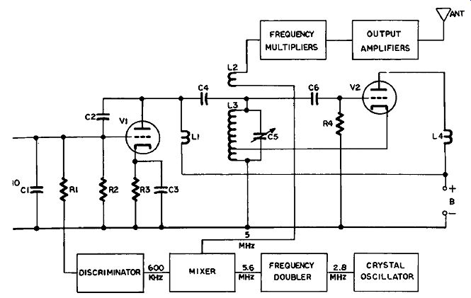
Figure 5.3 Reactance Circuit and Oscillator for FM Transmitter
... degeneration, as explained in section 2. L1 is an RF choke, to keep the carrier signal out of the power supply. C4 is a DC blocking capacitor to keep the power supply from being short-circuited through L3.
The modulated carrier is coupled inductively from L3 to L2, and goes via frequency multipliers (see section 12) and output amplifiers (see section 3) to the antenna. If the modulated carrier is 5 mega hertz, as in Figure 5.3, the frequency multipliers will raise it to the radio frequency. In the FM broadcast band this is between 88 and 108 megahertz.
The carrier frequency of an FM broadcasting station must not be allowed to drift more than 2 kilohertz from its assigned frequency.
This means that a broadcast frequency of 100 megahertz (approximately in the middle of the band) must be held to a tolerance of ±0.002 percent. Only a crystal-controlled oscillator can be this stable.
Obviously, you cannot control a variable-frequency oscillator directly with a crystal as it would no longer be variable; so an indirect method must be used.
A separate crystal oscillator (see section 4) is provided to supply a very stable signal at a slightly higher frequency than the resting frequency of the Hartley oscillator. The two frequencies are combined in a mixer (discussed later in this section), and the difference signal is applied to a discriminator.
If the carrier begins to drift the discriminator converts the change in the difference-signal into a DC voltage, which changes the bias on the grid of V1 so as to bring the resonant frequency of the Hartley oscillator back to its proper value. Audio voltage feedback is filtered out of the DC voltage from the discriminator by C1 and R1.
Circuit Variations
A reactance can be made inductive instead of capacitive by substituting an inductor for C2. In this case the circuit will have inductive characteristics: the voltage will lead the current. The resonant frequency of the oscillator will vary with the varying inductance of the reactance circuit.
An inductive effect will also be obtained by interchanging R2 with C2, and making R2 ten times the value of C2 at the resonant frequency. The grid voltage now appears across C2, and because it lags the current, the plate current of V1 will lag the oscillator voltage, so that the reactance circuit will look like an inductor to L3.
Similarly, if an inductor is used in the place of C2, now between the grid and low side of the circuit, the reactance circuit will present a capacitive appearance to L3.
In the three variations just mentioned an additional DC blocking capacitor is required in series with the inductor or resistor connected between the plate and grid of V1. A large value capacitor is used so it will offer virtually no reactance to the resonant frequency, while keeping the plate voltage from reaching the grid.
ARMSTRONG BALANCED MODULATOR
Another method of FM is shown in Figure 5.4, which illustrates the Armstrong balanced modulator.
Distinguishing Features
The balanced modulator in the upper part of the schematic consists of a push-pull output stage which resembles an audio power amplifier (see section 3) with its output coupled to a single-tube audio voltage amplifier.
It differs from an actual audio push-pull amplifier, however, be cause the audio output transformer is replaced by the three coils L1, L2 and L3; and the screen grids of V1 and V2 are connected to opposite ends of the secondary of the modulation transformer T1.
The audio input is connected to the primary. The output from an oscillator is connected to the input. (There may be an amplifier between the oscillator and the balanced modulator.) Uses It is used in FM transmitters.
Detailed Analysis
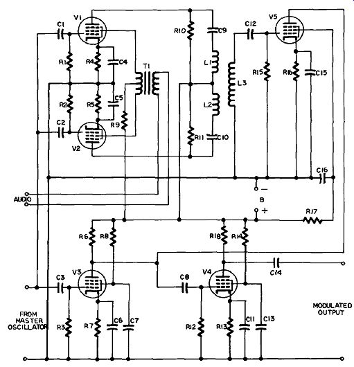
Figure 5.4
DC Subcircuits: In Figure 5.4 electron low is as follows:
V1: From B- via R4 to the cathode; from the plate via R10 back to B+; and from the screen grid via the upper half of T1 and R9 back to B-f.
V2: From B- via R5 to the cathode; from the plate via R11 back to B+; and from the screen grid via the lower half of T1 and R9 back to B+.
V3: From B- via R7 to the cathode; from the plate via R6 back to Band from the screen grid via R8 back to B+.
V4: From B- via R13 to the cathode; from the plate via R18 back to B+; and from the screen grid via R14 back to B+.
V5: From B- via R16 to the cathode; from the plate via R6 back to B+; and from the screen grid via R17 back to B+.
Grid bias for all tubes is determined by their cathode resistors.
AC Subcircuits: The master oscillator is a crystal oscillator with a tightly controlled frequency, typically of 200 kilohertz, so you can see these amplifiers will not be handling RF. The oscillator signal is applied to the input of V3 and also to the grids of V1 and V2. The input circuit of V3 is identical with that of similar audio voltage amplifiers described in section 2.
The oscillator signal is applied simultaneously to each grid of V1 and V2 without inversion; so as far as this signal is concerned the outputs of both tubes are in phase.
The audio input is obtained from an audio amplifier section in which the audio has been amplified and pre-emphasized (see next circuit in this section), hence this amplifier is called a correction amplifier. The audio signal from the correction amplifier is applied to the screen grids of V1 and V2 via the transformer T1. The secondary of T1 is tapped, so that when the upper end of it swings positively in respect to the tap the lower end is swinging negatively; consequently the screen grids receive identical signals of opposite phase.
Notice that these screen grids are not bypassed by capacitors, so the audio voltage appears on them and controls the plate current in each tube.
When no audio signal is present, equally amplified 200-kilohertz signals from V1 and V2 low in opposite directions through L1 and L2, and because their induced magnetic fields are of opposite polarity they cancel each other, so no voltage is induced in L3 by the unmodulated carrier.
However, when an audio signal appears on the screen grids of V1 and V2 the tube receiving a positive-swinging signal will amplify more (because the grid will be more positive) than the other, with its negative-going signal, which will conduct less. Consequently, the 200-kilohertz signals appearing in L1 and L2 will be of unequal amplitude, and so a voltage will be induced in L3 by the stronger one.
As this alternates between L1 and L2 the polarity of the voltage of the signal induced in L3 will alternate also.
The values of L1-C9 and L2-C10 have been chosen so that the currents in them are in phase with the voltage output from V1 and V2, but the voltage induced in L3 lags by 90 degrees.
This signal in L3 consists only of the sidebands, because, as you saw, the carrier by itself cannot induce any signal in L3. After amplification in V5’s circuit they are recombined with the carrier at the output of V3. Because their phase is shifting back and forth at the audio rate, they cause the phase of the carrier to do the same.
However, when the phase shifts, the frequency shifts also, so the carrier signal that arrives at the grid of V4 is frequency modulated.
V4's circuit is designed to limit the amplitude of the signal to get rid of any AM, some of which is bound to be present at this point.
The path followed by the signal from here to the antenna is similar to that in the reactance-modulator circuit described previously. however, in practical systems a converter stage will also be used, with a local oscillator which must be crystal-controlled as well. This is to overcome difficulties arising from using an excessive number of frequency-multiplication stages. Converter circuits are discussed later in this section.
PRE-EMPHASIS CIRCUIT
Before leaving this section on FM circuits we must consider the pre-emphasis circuit illustrated in Figure 5.5. In appearance this is an ordinary audio voltage amplifier. However, the value of C1 has been chosen to offer considerable reactance to lower frequencies. This reactance tapers of as the frequency increases, becoming virtually ...
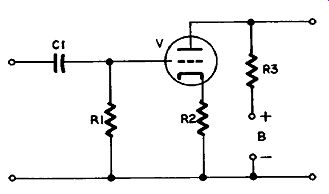
Figure 5.5 Pre-Emphasis Circuit
... zero at the permitted upper audio limit of 15 kilohertz. As a result, the higher frequencies are emphasized, which gives a better signal-to noise ratio in transmission. The value of R1 that gives the best performance is one that makes the C1-R1 time-constant 75 microseconds.
You will see that in FM receivers a corresponding de-emphasis circuit must be provided to restore the upper audio frequencies to their original level.
PHASE MODULATION
Phase modulation affects everyone who watches color television.
The monochrome TV signal carries video by AM and audio by FM.
The color signal includes color by PM.
In FM we vary the frequency of the carrier in accordance with the amplitude of the modulating signal, but in PM we vary its phase angle. This brings up the subject of vectors, which we must touch on briefly before going any further.
VECTORS
If we take a piece of paper and designate the top edge as north, and the left-hand side as west, and make a pencil dot in the middle for a ship, we can draw a vertical line from this dot to represent the ship traveling north, or a horizontal line to represent it traveling west.
We have done this in Figure 5.6.
We can also represent the ship’s speed. If we choose a scale of 10 knots to an inch, and the ship’s speed is 20 knots, we shall draw the lines two inches long.
Suppose our ship is traveling northwest. Its course and speed are now represented by a two-inch line sloping up toward the left-hand upper corner of the paper, midway between the other two lines.
The point at the end of this line also shows that at the end of one hour the ship is 20 nautical miles northwest of its starting position.
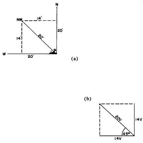
Figure 5.6 Vectors
By measuring along the dotted lines, we can also say that the ship is now 14 miles north and 14 miles west of its starting point. Since it got there in one hour we could also say that the ship' s speed was 14 knots to the north and 14 knots to the west, resulting in a total speed of 20 knots to the northwest.
In this diagram the three courses and speeds of the ship have been represented by lines drawn to show direction and velocity. Such lines are called vectors. In electronics, vectors are also used to show angles and voltages.
If, instead of compass headings and speeds, we substitute angles (measured clockwise from W) and voltages, we could use this diagram to show that two vectors, one of 14 volts at 0 degrees and one of 14 volts at 90 degrees, result in a vector of 20 volts at 45 degrees.
This is called vector addition. It is not the same as arithmetical addition, where 14 + 14 = 28, because the quantities added do not lie in the same straight line.
If they did they would be in phase. Where they do not the angle between them is called a phase angle.
COLOR MODULATION
In transmitting the color in color television a subcarrier is used.
The space between the video and sound carriers in monochrome TV is occupied by the upper sideband of the video signal, which consists of groups of frequencies centered on harmonics of the line frequency, with spaces between. The color subcarrier has a frequency of 3.579545 megahertz (usually approximated to 3.58 MHz), which places it in the gap between the 227th and 228th harmonic of the line frequency.
Harmonics of the color subcarrier fall into other spaces on either side of this one, since they are also separated by intervals equal to the line frequency (15.734264 kHz). In this way we can transmit a second signal interleaved within the main one.
This color signal has been modulated by shifting its phase according to the wavelength of the color. However, as we have just seen, a phase vector can be broken down into two vectors at right angles to each other. This is done by using a doubly balanced modulator.
DOUBLY BALANCED MODULATOR
Figure 5.7 shows a doubly balanced modulator that can be used to encode the 3.58-megahertz subcarrier with color information.
Distinguishing Features
You will notice a distinct similarity between this circuit and the Armstrong balanced modulator in Figure 5.4. However, the modulating signal is actually fed to a phase-inverter triode (V1), from which two outputs of opposite phase go to the grids of V2 and V3.
The carrier signal is applied to the third grids of these tubes, so the inputs are different from those of Figure 5.4.
Uses
TV color information encoding.
Detailed Analysis
DC Subcircuit: In Figure 5.7 electron low is from B- (the low side of the circuit) via R2, V1 and R1 to B+; and via R6, both V2 and V3, and R3 to B+. Connections from the screen grids of V2 and V3 to B+ have been omitted.
AC Input: The color information derived from the red, green and blue cameras was changed by previous circuits into the Y,
I and Q signals. The Y, being equivalent to the monochrome of black-and white pictures, bypasses this circuit. The I signal is fed to one of two doubly balanced modulators, the Q signal to the other.
The I Signal is used to transmit colors in the orange and cyan regions, and since more line detail is visible in these colors it is given a greater bandwidth (1.3 MHz). We will deal with this signal first.
When the I signal on the grid of V1 is positive, it will be reproduced by this tube as a positive signal on its cathode and a negative signal on its plate. (See section 3 for more about phase inverters.) Consequently two signals of opposite phase reach the grids of V2 and V3. V2’s grid will go more negative and V3's will go more positive.
V2 will therefore conduct less, and V3 will conduct more.
Meanwhile a 3.58-megahertz signal is being applied to the primary
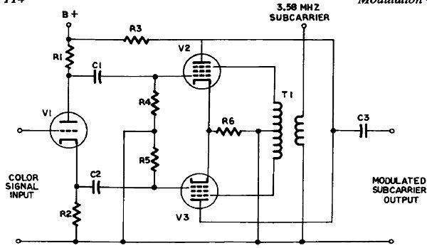
Figure 5.7 Doubly Balanced Modulator of T1. T1's secondary has a centertap
connected to the low side of the circuit. When the signal at the upper end
of the secondary is positive, that at the lower end will be negative, and vice-versa.
AC Output: Because V2's gain has been decreased by the negative voltage on its control grid, the amplitude of the 3.58-megahertz signal appearing at its plate will be lower than that at the plate of V3, where the gain has increased.
The output from V3 will not only be greater, but will also be of opposite phase to the subcarrier input.
A signal consisting of the excess of V3's output over that of V2 will be coupled out through C3.
The same action takes place when the input to V1 is negative, except that the output signal is now in phase with the subcarrier.
The Q Signal: In the other doubly balanced modulator, the Q signal is applied to V1, and the operation of the circuit is identical.
However, the phase of the subcarrier applied to this circuit is 90° different from the other. Consequently its output is also 90° different. The bandwidth of this signal is also less (.4 MHz), as colors other than those in the I signal have less visible detail.
In our brief discussion of vectors you saw how two vectors at a 90° angle would add to give a resultant vector. The angle of this vector would depend upon the values (in this case amplitudes) of the first two. This is illustrated in Figure 5.8, where the red, blue and green vectors are shown as the result of adding different I and Q modulation ...
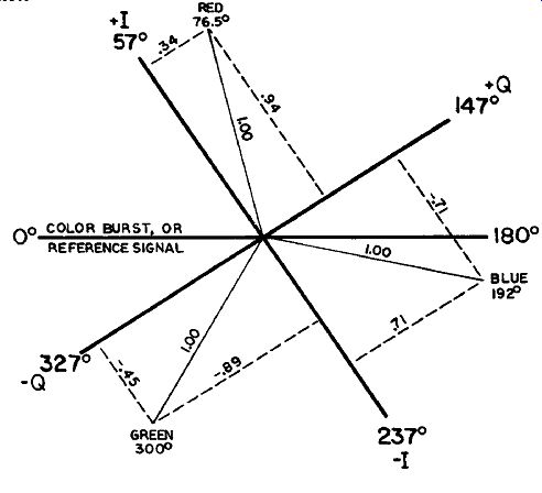
Figure 5.8 Color-Signal Phase Relationships
...amplitudes. The outputs of the two doubly balanced modulators are actually combined in this way, and since their amplitudes are rising and falling, and varying between being in-phases and being of opposite phase to their subcarriers, you can see that the resultant vector is swinging back and forth around the center like the hand of a seriously deranged clock. Each direction it points to is a different color, of course, so that in this way the phase angle of the subcarrier is made to vary in accordance with the color information.
As already mentioned, more detail is visible in the orange and cyan portions of a scene than in those of other colors, and the I signal, with greater bandwidth, is used to transmit this part of the spectrum. Since the phase angle for orange is 57° and that for cyan approximately 180° the opposite, the I subcarrier is delayed by this angle before being applied to the I modulator. Consequently the Q subcarrier is delayed 147° (57 + 90) before being applied to the Q modulator. The color bursts, however, are not phase-shifted.
Don’t forget that the Y signal bypasses the color modulators. Yet it contains the "whiteness" information for the picture. In the receiver it is recombined with the color signals so that the colors on the screen have the proper saturation as well as hue.
PULSE MODULATION
Pulse modulation is another way of sending more than one signal on the same carrier. It can employ any of the foregoing methods of modulation, but generally AM is used. A continuous modulating signal is chopped into pulses before modulating the carrier. You could compare this to a motion picture, in which the moving scene is recorded by a series of snapshots. If this is done rapidly enough, they blend together on the screen so that the eye does not detect the individual frames. In pulse modulation the spaces between the pulses are used for other pulses. As long as proper synchronization is maintained, the receiver can separate the channels and reproduce the separate signals as well as if they had been sent on individual carriers. This process is called multiplexing.
Uses
Pulse modulation is used to enable a single computer to control several processes simultaneously. The high-speed pulses from the different locations are kept in rigid synchronization by a "clock" running at microsecond speed. The computer accepts their inputs in rotation, called time-sharing, so that each stream of data is kept separate. The computer , s outputs are made in the same way.
Pulse modulation is also used in telemetering. This is the method of transmitting on one carrier data from several sensing instruments from a space ship to earth. As you can see, it is practically the same as time-sharing or multiplexing.
Circuits
The circuits used in pulse modulation are similar to those used for AM, FM or PM. The essential difference is that the modulating signal must be chopped, or gated (see section 9) to form it into pulses.
The main types of pulse modulation are:
(1) Puke-amplitude modulation (PAM): only amplitude of pulse varies.
(2) Pulse-width modulation (PWM): only width of pulse varies.
(3) Pulse-time modulation (PTM): only space between pulses varies.
(4) Pulse-code modulation (PCM): combination of (2) and (3).
MIXER CIRCUIT
Figure 5.9 shows a mixer circuit using a pentode tube.
Distinguishing Features
A mixer resembles other RF or IF voltage amplifiers (compare with Figure 2.22), having a grounded-cathode or common-emitter circuit.
It is distinguished from other RF or IF voltage amplifiers by having an additional input to the grid from an oscillator. This oscillator, which is often a Hartley or Colpitts type (see section 4), is known as a local oscillator.
Uses
A mixer is used in a radio receiver, TV tuner or similar application, in order to change the frequency of the incoming RF signal to the IF frequency of the following IF stage(s).
Detailed Analysis
DC Subcircuit: In Figure 5.9 electron low is from B- via R1 to the cathode of V. From V’s plate, current returns to B+ via L3, and from the screen grid via R2.
The value of R1 is chosen to bias the tube so that it operates on the non-linear portion of its characteristic curve, which makes it act ...
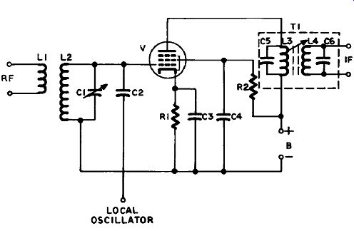
Figure 5.9 Mixer like a detector.
... , consequently, in a radio receiver, this circuit is often called the " first detector." However, audio information is not removed here but at a later stage, sometimes referred to as the " second detector," which will be discussed in section 6.
AC Input Subcircuit: The resonant circuit L2-C1 is tuned to be resonant at the frequency of the radio or TV signal it is desired to receive. This signal is present in L1, is inductively coupled into L2, and gets a resonant-voltage step-up in the process. It is then applied between the control grid and cathode of V.
As you just saw, the tube is operating on the non-linear portion of its characteristic curve (see Appendix). Consequently, when the grid voltage swings in a negative direction the tube is cut off; it con ducts only on the positive swings. This is similar to the operation of the RF amplifier used in the grid-modulation circuit discussed earlier in this section. However, that was a high-power amplifier, whereas this is a low-power voltage amplifier.
The reason for operating the tube near the cut-of point is because it is then able to modulate one signal with another. The oscillator signal, which is applied to the grid by way of C2, "beats " with the incoming RF signal to produce upper and lower sidebands that are equal to the sum and difference frequencies of the two signals. This process is called heterodyning.
If the incoming signal is at a frequency of, say 1070 kilohertz, and the local oscillator is operating at 1520 kilohertz, the upper sideband frequency will be 2590 kilohertz (1070 + 1520), and the lower side band 450 kilohertz (1520 - 1070). If the incoming signal was al ready modulated by (for illustration) a single frequency of 1 kilohertz, it will have sidebands of its own at 1069 and 1071 kilohertz.
These will give sidebands on sidebands: upper sidebands of 2589 and 2591 kilohertz; and lower sidebands of 449 and 451 kilohertz. Of course, in a real transmission there are many more sidebands, all of which will appear in the output with new upper and lower sidebands also.
We’re only interested in the lower sidebands around 450 kilohertz.
In AM broadcasting most stations are allotted a bandwidth extending 5 kilohertz above and below the carrier frequency. (A few stations are allowed up to 15 kilohertz, but there are not many of these "clear channel " stations.) The IF transformer T1 is made resonant at 450 kilohertz, with a broad enough bandwidth to allow the 450-kilohertz carrier and its sidebands to pass, but excluding the rest. (See also section on IF amplifiers in section 2.) This type of radio receiver is called a superheterodyne receiver, and is almost the only type used today.
Circuit Variations
Mixers using transistors are found with circuits similar to that in Figure 5.9. They may also be found with dual tubes, containing a triode (for the oscillator) and a pentode (for the mixer) in one envelope. Such a tube might be employed in the next stage after the RF cascode amplifier shown in Figure 2.25.
CONVERTERS
Figures 5.10 and 5.11 are examples of converter circuits, in which mixer and local oscillator are combined in one circuit.
Distinguishing Features
a. Vacuum-tube converters use pentagrid tubes (tubes with five grids, also called heptodes because there are seven electrodes). A penta grid tube is enough to identify a converter. However, it is usually also connected in a circuit with a tunable resonant input which is ganged to track with the oscillator resonant circuit; and an IF trans- former is provided in the output, as in the mixer circuit discussed previously.
b. Transistor converters are just as easy to identify, even though the transistors do not have five grids, since they are connected in the same kind of circuit. In the example given in Figure 5.11 a loop stick antenna with a ferrite core (L1 and L2) is also shown, a feature of practically all transistor radios today.
Uses
Just about all AM broadcast receivers use converters today. They are also used in many other types of receiver, though sometimes preceded by an RF amplifier stage, as, for example, in TV receivers.
Detailed Analysis
DC Subcircuits: In Figure 5.10 electron low is from B- via the lower part of L3 to the cathode of V. From the plate it returns through L4 to B+, and from grids numbers 2 and 4 via R2 to B+.
In Figure 5.11 electron low is from the negative pole of the battery through R3 to Q’s emitter, and from the collector via L5, the lower portion of L4 and R2, back to the positive pole of the battery. Bias is stabilized by R3 and R1.
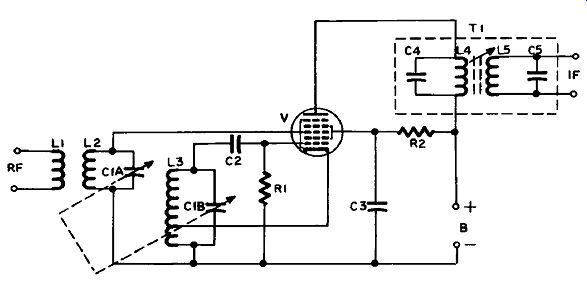
Figure 5.10 Pentagrid Converter
AC Subcircuits: Each circuit has two inputs, the oscillator and the external RF. The oscillator in each case is a Hartley oscillator (some times a Colpitts is used). That in the tube circuit (Figure 5.10) is identical with the circuit in Figure 4.1. The transistor circuit differs a little, but you’ll see why that is when we get to it.
In the pentagrid tube the grids are numbered from 1 through 5, starting from the one next to the cathode. Grids 2 and 4 are connected internally, so as to shield the third grid and minimize coupling between the circuits. Grids 2 and 4 are maintained at signal ground (AC zero) potential by C3. Grid No. 5 is a suppressor grid, and is connected internally to the cathode as shown, or externally to the low side of the circuit.
In Figure 4.1 the tube is a triode. In the pentagrid in Figure 5.10 the function of the triode is performed by the cathode, No. 1 grid and No. 2 grid (No. 2 grid acting as the triode plate). The electron current lowing from the cathode to No. 2 grid is made to vary at the oscillator frequency by the oscillating voltage on the No. 1 grid. The operation of the Hartley oscillator is explained in section 4, so will not be repeated here. However, the No. 2 grid does not present a complete barrier to electrons. Attracted by the higher positive potential of the plate, most of them pass on through grids 2, 3, 4 and 5.
As they pass through grid No. 3 the stream of electrons is modulated by the varying RF signal voltage on this grid. This results in the appearance, in the output stage, of the oscillator and RF carrier signal frequencies, together with all the sidebands, as already explained in the section on the mixer circuit preceding this.
T1 is an IF transformer tuned to let pass the IF frequency and its set of sidebands, while excluding the others.
The RF input may be from an external antenna or an internal loop antenna. In modern sets the ferrite loopstick L1 and L2 shown in Figure 5.11 is very popular for broadcast-band reception. It is tuned to resonance at the desired frequency by means of C1A, which is ganged with C1B (Figure 5.10). Usually a combined variable capacitor is used, in which both rotors share a common shaft, and turn together. This is to enable them to "track" or maintain a fixed difference frequency. The oscillator frequency must always be above that of the incoming RF frequency by the amount of the IF frequency, or there will be no difference frequency able to pass through to the IF stage.
C1 A, C1B and L3 are always provided with trimmer capacitors and adjustable ferrite slugs for exact alignment * for accurate tracking and tuning dial indication. These are shown in Figure 5.11 (C1A, C1C and L4), and are indicated in most schematics.
In the transistor converter, apart from the features already mentioned, we see that the oscillator signal is coupled inductively to the ...
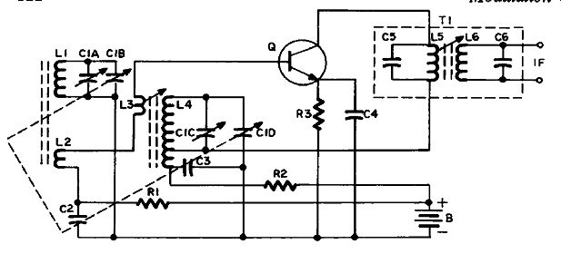
Figure 5.11 Transistor Converter
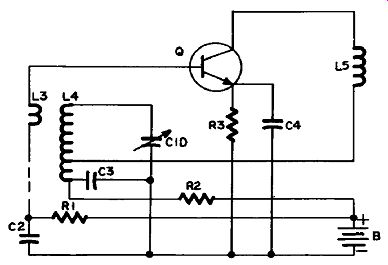
Figure 5.12 Transistor Converter-Oscillator Circuit
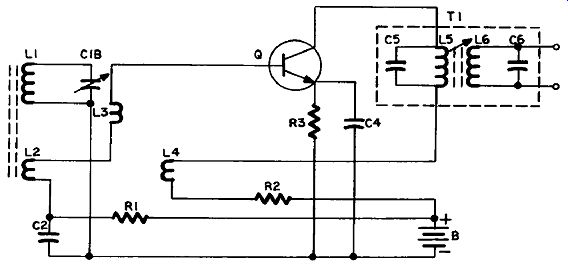
Figure 5.13
... base by L3 and L4 instead of capacitively by C2 as in Figure 5.10.
You will meet both types of coupling in these circuits.
The main difference between the pentagrid converter and the transistor converter is that in the tube we can see the cathode and grids 1 and 2 acting as a triode oscillator, and the cathode and grid 3 and the plate acting as a mixer, but in the transistor there are only the usual three elements to do everything.
At first you may wonder about this. However, there is no rule that says a transistor can only do one thing at a time. This one is a mixer and an oscillator simultaneously, just as if it were two entirely separate transistors. To make this clearer, Figure 5.11 has been redrawn in Figures 5.12 and 5.13 as a separate oscillator and mixer.
In Figure 5.12 you see a Hartley oscillator which only differs from that in Figure 4.2 by having the tap on L4 connected via L5 to the collector instead of to the emitter, and the oscillations of L4-C1D inductively coupled to the base by the "tickler" coil L3 instead of by a capacitor. These circuit variations do not change the principle of operation.
In Figure 5.13 you see that the mixer circuit is almost the same as that in Figure 5.9. If Figure 5.13 is superimposed on Figure 5.12 you get back Figure 5.11.
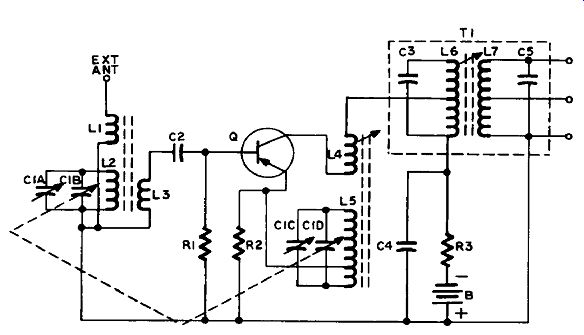
Figure 5.14 Transistor-Converter Circuit Variation
Circuit Variations
Pentagrid converters are pretty much standardized, but transistor circuits do offer some variety. An alternative to that shown in Figure 5.11 is shown in Figure 5.14.
As you can see, the main difference is that the "tickler" (L4) is now connected in the output circuit instead of in the input, while the oscillator resonant circuit is connected to the emitter instead of to the collector via the IF transformer. The net result is the same.
A connection for an optional external antenna is shown which is sometimes provided in the better type of receiver.
The collector of the transistor is connected to a centertap on the IF transformer, which is often done, as explained in the section on IF transistor amplifiers in section 2.
TROUBLESHOOTING CHART FOR MIXERS AND CONVERTERS
Tube Faulty or Tube Voltage Wrong
Wrong Alignment of Tuning Adjustment
-------------------